EP0402134A2 - Verzögerungsfehler-Testvorrichtung - Google Patents
Verzögerungsfehler-Testvorrichtung Download PDFInfo
- Publication number
- EP0402134A2 EP0402134A2 EP90306187A EP90306187A EP0402134A2 EP 0402134 A2 EP0402134 A2 EP 0402134A2 EP 90306187 A EP90306187 A EP 90306187A EP 90306187 A EP90306187 A EP 90306187A EP 0402134 A2 EP0402134 A2 EP 0402134A2
- Authority
- EP
- European Patent Office
- Prior art keywords
- input
- output
- test
- signal
- logic
- Prior art date
- Legal status (The legal status is an assumption and is not a legal conclusion. Google has not performed a legal analysis and makes no representation as to the accuracy of the status listed.)
- Granted
Links
Images






Classifications
-
- G—PHYSICS
- G01—MEASURING; TESTING
- G01R—MEASURING ELECTRIC VARIABLES; MEASURING MAGNETIC VARIABLES
- G01R31/00—Arrangements for testing electric properties; Arrangements for locating electric faults; Arrangements for electrical testing characterised by what is being tested not provided for elsewhere
- G01R31/28—Testing of electronic circuits, e.g. by signal tracer
- G01R31/317—Testing of digital circuits
- G01R31/3181—Functional testing
- G01R31/3185—Reconfiguring for testing, e.g. LSSD, partitioning
- G01R31/318533—Reconfiguring for testing, e.g. LSSD, partitioning using scanning techniques, e.g. LSSD, Boundary Scan, JTAG
- G01R31/318541—Scan latches or cell details
-
- G—PHYSICS
- G01—MEASURING; TESTING
- G01R—MEASURING ELECTRIC VARIABLES; MEASURING MAGNETIC VARIABLES
- G01R31/00—Arrangements for testing electric properties; Arrangements for locating electric faults; Arrangements for electrical testing characterised by what is being tested not provided for elsewhere
- G01R31/28—Testing of electronic circuits, e.g. by signal tracer
- G01R31/317—Testing of digital circuits
- G01R31/3181—Functional testing
- G01R31/3185—Reconfiguring for testing, e.g. LSSD, partitioning
- G01R31/318533—Reconfiguring for testing, e.g. LSSD, partitioning using scanning techniques, e.g. LSSD, Boundary Scan, JTAG
- G01R31/318552—Clock circuits details
-
- G—PHYSICS
- G01—MEASURING; TESTING
- G01R—MEASURING ELECTRIC VARIABLES; MEASURING MAGNETIC VARIABLES
- G01R31/00—Arrangements for testing electric properties; Arrangements for locating electric faults; Arrangements for electrical testing characterised by what is being tested not provided for elsewhere
- G01R31/28—Testing of electronic circuits, e.g. by signal tracer
- G01R31/317—Testing of digital circuits
- G01R31/3181—Functional testing
- G01R31/3185—Reconfiguring for testing, e.g. LSSD, partitioning
- G01R31/318533—Reconfiguring for testing, e.g. LSSD, partitioning using scanning techniques, e.g. LSSD, Boundary Scan, JTAG
- G01R31/318577—AC testing, e.g. current testing, burn-in
- G01R31/31858—Delay testing
Definitions
- a serial data path exists between the SDO of the input test cell 12i output and the SDI input of the output test cell 12j, creating an internal connection between the test cells for shifting data.
- the control bus signals (A, B, CLK, HOLD, and DMX) are connected to both test cells 12i and 12j, allowing both to operate together in a synchronous manner.
- the DINB signal is coupled to the ODI input of the test cell 12 and can be sampled during a load operation.
- the third multiplexer 36 is controlled by the DMX signal, also sent to the test cell 12.
- the LQ output of the test cell 12 is the output of the D latch 26 inside the test cell 12. The LQ output allows holding the DOUTA output signal constant in test mode during load and shift operations.
- the DINA output passes through the third multiplexer 36 and is output from the cell via the DOUTA output, establishing the normal data output path from the application logic 14 to the output buffer section of an I/0 buffer.
- the DINB input passes through the 2:1 multiplexer 28 within the test cell 12 and is output from the cell via the DOUTB output, establishing the normal data input path from the input buffer section of an I/0 buffer to the application logic 14.
- the first multiplexer 22 has six independent input signals.
- the SDI signal is input to two cascaded inverters 108 and 110.
- the resulting output from inverter 110 is then input to a transmission gate 112.
- a transmission gate is formed by tying both the sources and drains of a P channel transistor to an N channel transistor.
- the output of transmission gate 112 is tied to the output of transmission gate 114 and to the input to transmission gate 116.
- the output of transmission gate 116 is likewise tied to the output of transmission gate 122 and to the input to a pair of cascaded inverters 118 and 120. This output at inverter 120 represents the final output from multiplexer 22.
- the ODI input to multiplexer 22 is connected to transmission gate 114.
- the output of transmission gate 114 is tied to the output of transmission gate 112 and to the input to transmission gate 116.
- a third input to multiplexer 22 is the inverted output of latch 26. This signal is input into transmission gate 124.
- the output of transmission gate 124 is tied to the output of transmission gate 126 and to the input to transmission gate 122.
- a fourth input to multiplexer 22 is the output of the D flip-flop 24. This signal is input to transmission gate 126. The output of transmission gate 126 is then tied to the output of transmission gate 124 and to the input to transmission gate 122. The resultant output from transmission gate 122 is then tied to the output transmission gate 116.
- the B input to multiplexer 22 is also used as a select signal.
- the B input is connected to inverter 132.
- the output of inverter 132 is connected to inverter 134. Additionally, the output of inverter 132 is connected to the P channel gate of transmission gate 122 and the N channel gate of transmission gate 116.
- the output of inverter 134 is connected to the N channel gate of transmission gate 122 and the P channel gate of transmission gate 116.
- the D flip-flop 24 is connected to both a clock input CLK and the output of multiplexer 22. Within the D flip-flop 24, the clock signal is input to inverter 140, whose output is used to control the gate of N channel transistor 142. The clock signal is also used to control the gate of N channel transistor 144.
- the D input of D flip-flop 24 is connected to the first.source/drain of N channel transistor 142.
- the second source/drain of transistor 142 is connected to the input of inverter 146.
- the output of inverter 146 is connected to the first source/drain of N channel transistor 144 and also to the input of inverter 148.
- the output of inverter 148 is connected to the input of inverter 146.
- the second source/drain of transistor 144 is connected to the input of inverter 150.
- the output of inverter 150 is connected both to the input of inverter 152 and the input of inverter 154.
- the output of inverter 154 is connected to the input of inverter 150.
- the output of inverter 150 is also connected to the input of the transmission gate 126.
- the output of inverter 152 is the inverted output of the D flip-flop 24.
- the inverted output of D flip-flop 24 is then input to inverter 156.
- the output of inverter 156 is the SDO output of the test cell.
- the output of D flip-flop 24 (output of inverter 150) is connected to the D input of latch 26. This input is connected to the first source/drain of N channel transistor 160. The second source/drain of N channel transistor 160 is connected to the input of inverter 162. Within latch 26, the output of inverter 162 is connected to the input of inverter 166 and inverter 164. The output of inverter 166 is connected to the input of inverter 162. The output of inverter 162 also represents the inverted output of latch 26. As mentioned above, this inverted output is connected to multiplexer 22 through transmission gate 124. The output of inverter 164 represents the non-inverted output of the latch 26, which is connected to multiplexer 28. The latch 26 is also controlled by a hold voltage input to the base of N channel transistor 160.
- the second multiplexer 28 within the test cell has three separate inputs, DIN, the output of inverter 164, and DMX.
- the DIN signal is connected to the one gates of P channel transistor 170 and N channel transistor 172.
- the output of inverter 164 is connected to the gate of P channel transistor 182 and N channel transistor 184.
- the DMX input is connected to the gates of N channel transistor 174, 176 and 178, and also to the gate of P channel transistor 180.
- the first source/drain of N channel transistor 178 is connected to Vcc while the second source/drain is connected to node 196.
- the first source/drain of N channel transistor 176 is connected to ground while the second source/drain is connected to node 196.
- Node 196 is further connected to the gate of P channel transistor 188 and the gate of N channel transistor 186.
- the first source/drain of P channel transistors 188 and 180 are tied and connected to Vcc.
- the second source/drain of P channel transistors 188 and 180 are connected to the first source/drain of P channel transistors 182 and 170, respectively.
- the second source/drain of P channel transistors 182 and 170 are tied and connected to node 194.
- the first source/drain of N channel transistors 184 and 172 are tied and are further connected to node 194.
- the second source/drain of N channel transistors 184 and 172 are connected to the first source/drain of N channel transistors 174 and 186, respectively.
- the second source/drain of N channel transistors 174 and 186 are connected to ground.
- Node 196 is also connected to the gates of N channel transistors 192 and 190.
- the first source/drain of N channel transistor 192 is connected to Vcc.
- the second source/drain of N channel transistor 192 is connected to the first source/drain of N channel transistor 190 and this combined signal represents the DOUT signal of the test cell.
- the second source/drain of N channel transistor 190 is connected to ground.
- test cell 12 of the present invention may be enhanced through the use of cell libraries, in which additional circuitry may be provided on one or more of the test cells 12 used in IC 10 to provide an enhanced test circuit.
- a library of such circuits may be provided to enable a circuit designer to customize a particular IC 10.
- the maskable comparator logic section 200 comprises XOR gate 202 and a NAND 204.
- the XOR gate 202 has two inputs: a first input connected to the DIN and ODI inputs to the test cell 12 and a second input connected to an expected data (EXPD) signal.
- the NAND 204 also has two inputs: one input connected to the output of the XOR gate 202 and a second input connected to a compare mask (CMPMSK) signal.
- CMPMSK compare mask
- the output of the NAND gate 204 provides a compare output (CMPOUT) signal.
- the maskable comparator logic 200 provides a means to compare logic level appearing at the DIN input of the test cell 12 against a predetermined logic level appearing at the EXPD input. If the logic level on the DIN input and the EXPD input match, the output of the exclusive OR gate will driven low. If the logic level on the DIN input and the EXPD input do not match, the output of the exclusive OR gate will be driven high. A low level output (match condition) from the exclusive OR gate will cause the NAND gate to output a high level via the CMPOUT output. The high level output (no match) from the exclusive OR gate 202 will cause the NAND gate 204 to output a low logic level via the CMPOUT output, unless the CMPMSK input to the NAND gate 204 is at a low level.
- a high logic level on the CMPOUT output of the comparator logic section 200 indicates that the input or output boundary signal passing through this particular test cell is equal to an expected condition.
- the condition of one or more of the integrated circuits inputs and/or outputs may be irrelevant.
- the comparator logic 200 may be forced to mask off the compare operation and output a high level on the CMPOUT output regardless of the result of the compare operation.
- This capability allows for "Don't Care" comparison conditions to be set around the boundary of an integrated circuit design.
- the Don't Care condition is achieved by setting the CMPMSK of a particular test cell to a low logic level. All test cells having a low level applied to their CMPMSK input will output a high logic level from their CMPOUT output. By forcing the CMPOUT output high, the test cells with Don't Care conditions do not influence the overall result of a comparison taking place in other test cells at the boundary of an integrated circuit.
- test cells may be required to provide Pseudo-Random Pattern Generation (PRPG) and/or Parallel Signature Analysis (PSA) capabilities at the boundary of an integrated circuit to facilitate testing.
- PRPG Pseudo-Random Pattern Generation
- PSA Parallel Signature Analysis
- PRPG a series of serially interconnected test cells can be made to generate a pseudo-random output pattern sequence from the DOUT outputs.
- PSA a series of serially interconnected test cells can be made to compress the data appearing at the DIN input into a "signature" for testing purposes.
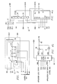
- FIGURE 7 A preferred implementation of a library cell capable of implementing PSA test logic is shown in FIGURE 7.
- the inputs and output of the base test cell 12 comprises the signals described in connection with FIGURE 2.
- the PSA logic section 206 receives two input signals, Data Mask (DATMSK) and PSA Enable (PSAENA).
- DATMSK and PSAENA inputs are extensions of the control bus.
- the PSA logic section 206 comprises an Exclusive OR gate 208 and two NAND gates, 210 and 212.
- the NAND 210 is connected to the DATMSK signal and the DIN input signal.
- the NAND gate 212 is connected to the PSAENA signal and the SDI signal.
- the outputs of the NAND gate 210 and 212 are connected to the inputs of the Exclusive OR gate 208.
- the output the Exclusive OR gate is connected to the ODI input of the base test cell 12.
- the PSA logic section 206 When the PSA logic section 206 is attached to the base cell 12, the normal connection of the ODI input to the DIN input is modified such that it is no longer a direct interconnect. However, the base function of capturing test data during a load operation via the ODI input is still valid, but addition rules set forth below and signal routing is required to accommodate the load operation via the PSA test logic. All other functions (idle, shift and toggle) and their required cell to cell interconnects remain the same.
- the DATMSK and PSAENA inputs to the logic section 206 are set to a high and low logic level, respectively.
- the PSA logic section provides a routing path from the DIN input, through the NAND gate 210 and the Exclusive OR gate 208 to the ODI input of the base test cell 12.
- the test cell 12 captures the logic level on the DIN input via the routing channel through the PSA logic section 206.
- the PSA logic section 206 provides a means to mask off the effect of the DIN input on the Exclusive OR operation.
- the masking is achieved by setting the MSKDAT input low while leaving the PSAENA input high.
- the PSA logic section 206 couples the SDI input to the ODI input of the test cell 12 and only the value of a preceding cell's SDO output is sampled and stored in the test cell 12. This capability allows masking out the signal attached to the DIN input of one or more of the test cells during a PSA operation at the boundary of an integrated circuit.
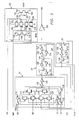
- serial data enters PSDI and flows through the test cells and out PSDO.
- the multiplexer 222 at the input of first test circuit 220a selects the feedback result (FBR) signal to be connected to the SDI input of the first test circuit 220a.
- the Programmable Polynomial Tap logic in the test circuits 220a-d in combination with the FBI and FBO wiring interconnects, forms the Exclusive OR feedback network required for PRPG and PSA operations. If the PTENA input of a test circuit is high, the logic state of test cell 12 of that test circuit 220 is included in the feedback network. If the PTENA input to a test circuit is low, the logic state of the test cell 12 of that test circuit is not included in the feedback network.
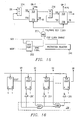
- test circuitry may be designed to include a test interface and a boundary scan path comprised of test cells 12.
- test circuitry may be designed to include a test interface and a boundary scan path comprised of test cells 12.
- test cell 240 The output of test cell 240 is connected to the output buffer 238 for tristate operation.
- the output of test cell 242 is connected to the clock input of register 234.
- the SDI signal from outside the test device 236 is received by the test cell 240, a scan bypass register 244 and an instruction register 246.
- a scan data path exists through the test cell 240, test cell 242, the input TCR 232 and the output TCR 236.
- Serial data output of the output TCR 236 is connected to a multiplexer 248 along with the output of the scan bypass 244.
- the multiplexer 248 receives a scan path select signal from the instruction register 246.
- the output of the multiplexer 248 is connected to a multiplexer 250 along with an output from the instruction register 246.
- the TCRs 232 and 236 comprise a plurality of test circuits based on the test cell 12, as discussed previously. Typically, the TCRs 232 and 236 will be formed from a plurality of test circuits with PRPG/PSA and/or programmable polynomial tap logic sections.
- the test cells 240 and 242 are typically base test cells 12 without additional circuitry.
- the control circuitry to the test cells 240 and 242 and TCRs 232 and 236 is not shown; however, a control bus would be connected to each cell for serial data shifting and test circuit control.
- a "boundary data sample instruction" may be installed in the instruction register 242.
- the boundary data sample instruction allows data and control to pass freely through the boundary scan path while the SCK and MODE inputs cause the boundary scan path to capture the logic state existing at their inputs. Once the boundary data has been captured, additional external control is issued via the SCK and MODE inputs to cause the boundary scan path to shift out the captured data for inspection via the SDO pin.
- a "control boundary outputs to a logic 1 or 0 instruction” allows the boundary scan path to take control of the I/0 signals in order to apply a prescanned test control pattern from the outputs of the test cells 240 and 242 and TCRs 232 and 236.
- the boundary scan path Prior to performing this test instruction, the boundary scan path will have been scanned to install the test control output pattern to be applied by the instruction.
- the scan bypass register is coupled to the SDI and SDO pins in order to form a single bit scan path through the test device during data register scan operations.
- test cell 12 of the driving integrated circuit 264 has the capability to toggle between opposite logic states, highs and lows, in response to the CLK signal.
- test cell 12 of the receiving integrated circuit 266 has the ability to sample data at its input in response to the CLK signal.
- a single toggle/sample instruction input to the test interfaces 268 of each integrated circuit 264 and 266 may be used to toggle the output of the driving integrated circuit 264 on a first clock edge and to sample the input of the receiving integrated circuit on the next clock edge.
- the present invention is described herein using a rising clock edge to initiated the toggle operation and a falling clock edge to initiate the sample operation; however, a falling edge toggle and a rising edge sample could be used as well.
- FIGURE 19 illustrates the present invention used in connection with open collector outputs.
- open collector outputs the transition from high to low is extremely fast because of the active pull-down of the signal, while the transition from low to high is relatively gradual, due to the passive pull-up resistor.
- FIGURE 19 timing signals illustrating an open collector output delay measurement are shown.
- the CLK signal has a falling edge at 282, initiating a toggle from high to low on the OUT signal at 284. Shortly thereafter (assuming no additional delay), the input signal toggles at 286 from a high logic level to a low logic level.
- the state of the IN signal is sampled into the test cell 12 of the receiving integrated circuit 266.
- FIGURE 20 Although a single signal delay measurement has been described in prior examples. The technique described herein applies to any number of input and output signals interconnected between one or more ICs in a circuit.
- FIGURE 20 two ICs 290 and 291 are shown connected together via a delay source 270.
- This example is similar to the one shown in FIGURE 17 except that multiple outputs (OUT1, OUT2, OUT3, OUTn) signals are driven by IC 290 through a delay source 270 to multiple inputs (IN1, IN2, IN3, INn) received by IC 291. Also shown in the dotted signal paths is the possibility of other ICs in the circuit driving input signals into the delay source and receiving outputs from the delay source.
- the delay testing procedure for the circuit in FIGURE 20 is similar to the one described in FIGURE 17, except that multiple signal delay paths are tested simultaneously.
- test cell 12 driving the OUT2 output When delay testing is performed on the signal path from the OUT1 output of IC 292 to the IN input of IC 293, test cell 12 driving the OUT2 output is loaded to output a logic high. Also test cell 12 driving the OUT2 output receives control to remain in the idle state so that when the CLK input is applied from control bus 17 it continues to output a high logic state. Test cell 12 driving the OUT1 output is set to a predetermined logic state and receives control to toggle during one edge of the CLK input while the test cell 12 of IC 293 receiving the IN input samples the toggled logic state on the next opposite CLK edge.
Landscapes
- Engineering & Computer Science (AREA)
- General Engineering & Computer Science (AREA)
- Physics & Mathematics (AREA)
- General Physics & Mathematics (AREA)
- Power Engineering (AREA)
- Tests Of Electronic Circuits (AREA)
- Semiconductor Integrated Circuits (AREA)
Applications Claiming Priority (2)
| Application Number | Priority Date | Filing Date | Title |
|---|---|---|---|
| US07/364,915 US5056094A (en) | 1989-06-09 | 1989-06-09 | Delay fault testing method and apparatus |
| US364915 | 1989-06-09 |
Publications (3)
| Publication Number | Publication Date |
|---|---|
| EP0402134A2 true EP0402134A2 (de) | 1990-12-12 |
| EP0402134A3 EP0402134A3 (de) | 1991-09-04 |
| EP0402134B1 EP0402134B1 (de) | 1997-09-03 |
Family
ID=23436657
Family Applications (1)
| Application Number | Title | Priority Date | Filing Date |
|---|---|---|---|
| EP90306187A Expired - Lifetime EP0402134B1 (de) | 1989-06-09 | 1990-06-07 | Verzögerungsfehler-Testvorrichtung |
Country Status (4)
| Country | Link |
|---|---|
| US (1) | US5056094A (de) |
| EP (1) | EP0402134B1 (de) |
| JP (1) | JP3340736B2 (de) |
| DE (1) | DE69031362T2 (de) |
Cited By (11)
| Publication number | Priority date | Publication date | Assignee | Title |
|---|---|---|---|---|
| GB2256058A (en) * | 1991-05-23 | 1992-11-25 | Motorola Gmbh | Ieee 1149.1 boundary- scan architecture |
| EP0492913A3 (en) * | 1990-12-21 | 1993-07-14 | Compaq Computer Corporation | Signal conditioning logic |
| EP0585086A3 (de) * | 1992-08-27 | 1995-02-01 | American Telephone & Telegraph | Verfahren und Vorrichtung zum Selbsttesten auf Verzögerungsfehler. |
| EP0702239A3 (de) * | 1994-09-01 | 1996-04-03 | Sgs Thomson Microelectronics | |
| EP0768538A1 (de) * | 1995-10-13 | 1997-04-16 | Jtag Technologies B.V. | Verfahren, Prüfer und Schaltung zur Triggerimpulsbeauftragung einer Einrichtung |
| GB2327127A (en) * | 1997-05-27 | 1999-01-13 | Hewlett Packard Co | Test chip circuit for on-chip timing characterization |
| US5983378A (en) * | 1995-10-13 | 1999-11-09 | Jtag Technologies | Method tester and circuit for applying a pulse trigger to a unit to be triggered |
| FR2811433A1 (fr) * | 2000-07-08 | 2002-01-11 | Bosch Gmbh Robert | Procede et dispositif pour tester des circuits numeriques |
| WO2003027696A3 (de) * | 2001-09-21 | 2003-11-27 | Siemens Ag | Elektronischer baustein und verfahren zu dessen qualifizierungsmessung |
| EP1357388A3 (de) * | 2002-04-18 | 2004-03-17 | Lsi Logic Corporation | Register zur Charakterisierung des Ein- und Ausgangs einer integrierten Schaltung |
| WO2005050232A1 (en) * | 2003-11-14 | 2005-06-02 | Integrated Device Technology, Inc. | Scan chain registers that utilize feedback paths within latch units to support toggling of latch unit outputs during enhanced delay fault testing |
Families Citing this family (59)
| Publication number | Priority date | Publication date | Assignee | Title |
|---|---|---|---|---|
| US7137048B2 (en) * | 2001-02-02 | 2006-11-14 | Rambus Inc. | Method and apparatus for evaluating and optimizing a signaling system |
| DE68928837T2 (de) * | 1988-09-07 | 1999-05-12 | Texas Instruments Inc., Dallas, Tex. | Prüf-Puffer/Register |
| US5483518A (en) | 1992-06-17 | 1996-01-09 | Texas Instruments Incorporated | Addressable shadow port and protocol for serial bus networks |
| US5056094A (en) | 1989-06-09 | 1991-10-08 | Texas Instruments Incorporated | Delay fault testing method and apparatus |
| JP3005250B2 (ja) | 1989-06-30 | 2000-01-31 | テキサス インスツルメンツ インコーポレイテツド | バスモニター集積回路 |
| US6675333B1 (en) | 1990-03-30 | 2004-01-06 | Texas Instruments Incorporated | Integrated circuit with serial I/O controller |
| JPH04140677A (ja) * | 1990-10-01 | 1992-05-14 | Toshiba Corp | 半導体集積回路 |
| US5210759A (en) * | 1990-11-19 | 1993-05-11 | Motorola, Inc. | Data processing system having scan testing using set latches for selectively observing test data |
| JP3073534B2 (ja) * | 1991-01-08 | 2000-08-07 | 株式会社東芝 | セルスイッチ結合網およびその試験方法 |
| US5271019A (en) * | 1991-03-15 | 1993-12-14 | Amdahl Corporation | Scannable system with addressable scan reset groups |
| US5533032A (en) * | 1991-10-28 | 1996-07-02 | Sequoia Semiconductor, Inc. | Built-in self-test global clock drive architecture |
| US5477545A (en) * | 1993-02-09 | 1995-12-19 | Lsi Logic Corporation | Method and apparatus for testing of core-cell based integrated circuits |
| US5422891A (en) * | 1993-07-23 | 1995-06-06 | Rutgers University | Robust delay fault built-in self-testing method and apparatus |
| US5583787A (en) * | 1994-03-08 | 1996-12-10 | Motorola Inc. | Method and data processing system for determining electrical circuit path delays |
| US5544175A (en) * | 1994-03-15 | 1996-08-06 | Hewlett-Packard Company | Method and apparatus for the capturing and characterization of high-speed digital information |
| US5600787A (en) * | 1994-05-31 | 1997-02-04 | Motorola, Inc. | Method and data processing system for verifying circuit test vectors |
| JPH08249359A (ja) * | 1995-03-09 | 1996-09-27 | Matsushita Electric Ind Co Ltd | 信号波形計算方法及び信号伝播時間計算方法 |
| US6055659A (en) * | 1999-02-26 | 2000-04-25 | Texas Instruments Incorporated | Boundary scan with latching output buffer and weak input buffer |
| US5596585A (en) * | 1995-06-07 | 1997-01-21 | Advanced Micro Devices, Inc. | Performance driven BIST technique |
| US5969538A (en) | 1996-10-31 | 1999-10-19 | Texas Instruments Incorporated | Semiconductor wafer with interconnect between dies for testing and a process of testing |
| WO1997021107A1 (en) * | 1995-12-05 | 1997-06-12 | Atg Technology, Inc. | Partial scan logic |
| US5648973A (en) * | 1996-02-06 | 1997-07-15 | Ast Research, Inc. | I/O toggle test method using JTAG |
| US6260165B1 (en) | 1996-10-18 | 2001-07-10 | Texas Instruments Incorporated | Accelerating scan test by re-using response data as stimulus data |
| US5886901A (en) * | 1997-01-07 | 1999-03-23 | Lsi Logic Corporation | Flip-flop for scan test chain |
| WO1998033163A1 (en) * | 1997-01-27 | 1998-07-30 | Koninklijke Philips Electronics N.V. | Method of manufacturing a liquid crystal display module |
| US6081913A (en) * | 1997-06-03 | 2000-06-27 | Sun Microsystems, Inc. | Method for ensuring mutual exclusivity of selected signals during application of test patterns |
| US6314470B1 (en) * | 1997-07-25 | 2001-11-06 | Hewlett Packard Company | System and method for asynchronously accessing a graphics system for graphics application evaluation and control |
| US6408413B1 (en) | 1998-02-18 | 2002-06-18 | Texas Instruments Incorporated | Hierarchical access of test access ports in embedded core integrated circuits |
| US6405335B1 (en) | 1998-02-25 | 2002-06-11 | Texas Instruments Incorporated | Position independent testing of circuits |
| US6185710B1 (en) | 1998-03-30 | 2001-02-06 | International Business Machines Corporation | High-performance IEEE1149.1-compliant boundary scan cell |
| GB9810512D0 (en) * | 1998-05-15 | 1998-07-15 | Sgs Thomson Microelectronics | Detecting communication errors across a chip boundary |
| US6560734B1 (en) | 1998-06-19 | 2003-05-06 | Texas Instruments Incorporated | IC with addressable test port |
| US6519729B1 (en) | 1998-06-27 | 2003-02-11 | Texas Instruments Incorporated | Reduced power testing with equally divided scan paths |
| JP2000258506A (ja) * | 1999-03-12 | 2000-09-22 | Mitsubishi Electric Corp | 半導体集積回路およびそのテストパターン生成方法 |
| US7058862B2 (en) | 2000-05-26 | 2006-06-06 | Texas Instruments Incorporated | Selecting different 1149.1 TAP domains from update-IR state |
| DE19938060B4 (de) * | 1999-08-12 | 2008-06-19 | Nokia Siemens Networks Gmbh & Co.Kg | Integrierte Schaltung mit einer Testeinrichtung und Verfahren zum Testen der Güte elektrischer Verbindungen der ingegrierten Schaltung |
| JP4789297B2 (ja) * | 1999-11-29 | 2011-10-12 | パナソニック株式会社 | 半導体集積回路のテストパターン生成方法 |
| US6728915B2 (en) | 2000-01-10 | 2004-04-27 | Texas Instruments Incorporated | IC with shared scan cells selectively connected in scan path |
| US6769080B2 (en) | 2000-03-09 | 2004-07-27 | Texas Instruments Incorporated | Scan circuit low power adapter with counter |
| US6567943B1 (en) * | 2000-04-07 | 2003-05-20 | International Business Machines Corporation | D flip-flop structure with flush path for high-speed boundary scan applications |
| US7490275B2 (en) | 2001-02-02 | 2009-02-10 | Rambus Inc. | Method and apparatus for evaluating and optimizing a signaling system |
| US6701476B2 (en) * | 2001-05-29 | 2004-03-02 | Motorola, Inc. | Test access mechanism for supporting a configurable built-in self-test circuit and method thereof |
| US20020194565A1 (en) * | 2001-06-18 | 2002-12-19 | Karim Arabi | Simultaneous built-in self-testing of multiple identical blocks of integrated circuitry |
| DE10201431C1 (de) * | 2002-01-16 | 2003-08-21 | Infineon Technologies Ag | Integrierte Schaltung und Verfahren zum Betrieb einer Testanordnung mit einer integrierten Schaltung |
| JP2003233639A (ja) * | 2002-02-06 | 2003-08-22 | Mitsubishi Electric Corp | 故障検証装置、故障検証方法および故障解析手法 |
| US6904576B2 (en) * | 2002-08-09 | 2005-06-07 | Synplicity, Inc. | Method and system for debugging using replicated logic |
| US7398445B2 (en) * | 2002-08-09 | 2008-07-08 | Synplicity, Inc. | Method and system for debug and test using replicated logic |
| US7213216B2 (en) * | 2002-08-09 | 2007-05-01 | Synplicity, Inc. | Method and system for debugging using replicated logic and trigger logic |
| US20040199838A1 (en) * | 2003-03-19 | 2004-10-07 | Rutkowski Paul William | Enhanced boundary-scan method and apparatus providing tester channel reduction |
| DE10335809B4 (de) * | 2003-08-05 | 2010-07-01 | Infineon Technologies Ag | Integrierte Schaltung mit einem zu testenden elektronischen Schaltkreis und Testsystem-Anordnung zum Testen der integrierten Schaltung |
| WO2007026191A1 (en) * | 2004-07-28 | 2007-03-08 | Koninklijke Philips Electronics, N.V. | Circuit interconnect testing arrangement and approach therefor |
| US7475309B2 (en) * | 2005-06-30 | 2009-01-06 | Intel Corporation | Parallel test mode for multi-core processors |
| JP2007011957A (ja) * | 2005-07-04 | 2007-01-18 | Nec Electronics Corp | 回路設計装置およびプログラム |
| US7348797B2 (en) | 2005-08-30 | 2008-03-25 | Texas Instruments Incorporated | Functional cells for automated I/O timing characterization of an integrated circuit |
| JP4299856B2 (ja) * | 2006-12-14 | 2009-07-22 | エルピーダメモリ株式会社 | 半導体装置 |
| JP2012026950A (ja) * | 2010-07-27 | 2012-02-09 | Sony Corp | 集積半導体装置 |
| US9454468B2 (en) * | 2014-06-27 | 2016-09-27 | Wipro Limited | Method and system for testing software |
| KR102546302B1 (ko) * | 2016-07-08 | 2023-06-21 | 삼성전자주식회사 | 클락 지터 측정 회로 및 이를 포함하는 반도체 장치 |
| US11749368B2 (en) * | 2019-12-27 | 2023-09-05 | Intel Corporation | Quick configurable universal register for a configurable integrated circuit die |
Family Cites Families (15)
| Publication number | Priority date | Publication date | Assignee | Title |
|---|---|---|---|---|
| US3873818A (en) * | 1973-10-29 | 1975-03-25 | Ibm | Electronic tester for testing devices having a high circuit density |
| US3976940A (en) * | 1975-02-25 | 1976-08-24 | Fairchild Camera And Instrument Corporation | Testing circuit |
| US4066882A (en) * | 1976-08-16 | 1978-01-03 | Grumman Aerospace Corporation | Digital stimulus generating and response measuring means |
| USRE31056E (en) * | 1977-03-23 | 1982-10-12 | Fairchild Camera & Instrument Corp. | Computer controlled high-speed circuit for testing electronic devices |
| US4146835A (en) * | 1978-03-08 | 1979-03-27 | Western Electric Co., Inc. | Testing the differential response times of a plurality of circuits |
| JP2561644B2 (ja) | 1983-10-31 | 1996-12-11 | 株式会社日立製作所 | タイミング信号発生器 |
| JPH0743733B2 (ja) * | 1985-12-11 | 1995-05-15 | 株式会社日立製作所 | 論理シミュレーション方法 |
| US4672307A (en) * | 1985-12-20 | 1987-06-09 | University Of Southern California | Simplified delay testing for LSI circuit faults |
| JPH0760400B2 (ja) * | 1986-01-07 | 1995-06-28 | 株式会社日立製作所 | 論理回路の診断方法 |
| US4777616A (en) * | 1986-05-12 | 1988-10-11 | Outlook Technology, Inc. | Increased resolution logic analyzer using asynchronous sampling |
| JP2556017B2 (ja) | 1987-01-17 | 1996-11-20 | 日本電気株式会社 | 論理集積回路 |
| JP2604606B2 (ja) | 1987-11-24 | 1997-04-30 | 株式会社アドバンテスト | 回路試験装置 |
| US4937826A (en) * | 1988-09-09 | 1990-06-26 | Crosscheck Technology, Inc. | Method and apparatus for sensing defects in integrated circuit elements |
| US5056094A (en) | 1989-06-09 | 1991-10-08 | Texas Instruments Incorporated | Delay fault testing method and apparatus |
| JP6252264B2 (ja) | 2014-03-12 | 2017-12-27 | 住友化学株式会社 | 高分子化合物およびそれを用いた有機半導体素子 |
-
1989
- 1989-06-09 US US07/364,915 patent/US5056094A/en not_active Expired - Lifetime
-
1990
- 1990-06-07 DE DE69031362T patent/DE69031362T2/de not_active Expired - Fee Related
- 1990-06-07 EP EP90306187A patent/EP0402134B1/de not_active Expired - Lifetime
- 1990-06-08 JP JP14889490A patent/JP3340736B2/ja not_active Expired - Fee Related
Cited By (16)
| Publication number | Priority date | Publication date | Assignee | Title |
|---|---|---|---|---|
| EP0492913A3 (en) * | 1990-12-21 | 1993-07-14 | Compaq Computer Corporation | Signal conditioning logic |
| US5448699A (en) * | 1990-12-21 | 1995-09-05 | Compaq Computer Corp. | Apparatus with leading edge delay circuit for selectively sending a delayed substitute version of a signal transmitted between an expansion card and a system bus |
| GB2256058A (en) * | 1991-05-23 | 1992-11-25 | Motorola Gmbh | Ieee 1149.1 boundary- scan architecture |
| EP0585086A3 (de) * | 1992-08-27 | 1995-02-01 | American Telephone & Telegraph | Verfahren und Vorrichtung zum Selbsttesten auf Verzögerungsfehler. |
| US5742617A (en) * | 1994-09-01 | 1998-04-21 | Sgs-Thomson Microelectronics Limited | Controller for implementing scan testing |
| EP0702239A3 (de) * | 1994-09-01 | 1996-04-03 | Sgs Thomson Microelectronics | |
| US5983378A (en) * | 1995-10-13 | 1999-11-09 | Jtag Technologies | Method tester and circuit for applying a pulse trigger to a unit to be triggered |
| EP0768538A1 (de) * | 1995-10-13 | 1997-04-16 | Jtag Technologies B.V. | Verfahren, Prüfer und Schaltung zur Triggerimpulsbeauftragung einer Einrichtung |
| GB2327127A (en) * | 1997-05-27 | 1999-01-13 | Hewlett Packard Co | Test chip circuit for on-chip timing characterization |
| GB2327127B (en) * | 1997-05-27 | 2002-04-03 | Hewlett Packard Co | Test chip circuit for on-chip timing characterization |
| FR2811433A1 (fr) * | 2000-07-08 | 2002-01-11 | Bosch Gmbh Robert | Procede et dispositif pour tester des circuits numeriques |
| WO2003027696A3 (de) * | 2001-09-21 | 2003-11-27 | Siemens Ag | Elektronischer baustein und verfahren zu dessen qualifizierungsmessung |
| EP1357388A3 (de) * | 2002-04-18 | 2004-03-17 | Lsi Logic Corporation | Register zur Charakterisierung des Ein- und Ausgangs einer integrierten Schaltung |
| US7028238B2 (en) | 2002-04-18 | 2006-04-11 | Lsi Logic Corporation | Input/output characterization chain for an integrated circuit |
| WO2005050232A1 (en) * | 2003-11-14 | 2005-06-02 | Integrated Device Technology, Inc. | Scan chain registers that utilize feedback paths within latch units to support toggling of latch unit outputs during enhanced delay fault testing |
| US7162673B2 (en) | 2003-11-14 | 2007-01-09 | Integrated Device Technology, Inc. | Scan chain registers that utilize feedback paths within latch units to support toggling of latch unit outputs during enhanced delay fault testing |
Also Published As
| Publication number | Publication date |
|---|---|
| DE69031362T2 (de) | 1998-01-08 |
| JP3340736B2 (ja) | 2002-11-05 |
| EP0402134A3 (de) | 1991-09-04 |
| EP0402134B1 (de) | 1997-09-03 |
| US5056094A (en) | 1991-10-08 |
| DE69031362D1 (de) | 1997-10-09 |
| JPH03103781A (ja) | 1991-04-30 |
Similar Documents
| Publication | Publication Date | Title |
|---|---|---|
| US5056094A (en) | Delay fault testing method and apparatus | |
| US6081916A (en) | IC with test cells having separate data and test paths | |
| US5495487A (en) | Testing buffer/register | |
| US5084874A (en) | Enhanced test circuit | |
| US6304987B1 (en) | Integrated test circuit | |
| US4669081A (en) | LSI fault insertion | |
| US5349587A (en) | Multiple clock rate test apparatus for testing digital systems | |
| US5606567A (en) | Delay testing of high-performance digital components by a slow-speed tester | |
| US4833676A (en) | Interleaved method and circuitry for testing for stuck open faults | |
| US6861867B2 (en) | Method and apparatus for built-in self-test of logic circuits with multiple clock domains | |
| US20030011396A1 (en) | Semiconductor device and test system therefor | |
| US4876501A (en) | Method and apparatus for high accuracy measurment of VLSI components | |
| EP0358371B1 (de) | Erweiterte Prüfschaltung | |
| US20050015689A1 (en) | Electronic component and method for measuring its qualification | |
| US5130989A (en) | Serial and parallel scan technique for improved testing of systolic arrays | |
| US20030200045A1 (en) | Input/output characterization chain for an integrated circuit | |
| US20050278593A1 (en) | Scan-test structure having increased effectiveness and related systems and methods | |
| Bhuyan et al. | Estimating Stuck at Coverage percentage through scan flops during scan | |
| US20240250668A1 (en) | Area, cost, and time-effective scan coverage improvement | |
| EP0286920A2 (de) | Verfahren und Einrichtung zur Prüfung von VLSI-Komponenten |
Legal Events
| Date | Code | Title | Description |
|---|---|---|---|
| PUAI | Public reference made under article 153(3) epc to a published international application that has entered the european phase |
Free format text: ORIGINAL CODE: 0009012 |
|
| AK | Designated contracting states |
Kind code of ref document: A2 Designated state(s): DE FR GB IT NL |
|
| PUAL | Search report despatched |
Free format text: ORIGINAL CODE: 0009013 |
|
| RHK1 | Main classification (correction) |
Ipc: G06F 11/22 |
|
| AK | Designated contracting states |
Kind code of ref document: A3 Designated state(s): DE FR GB IT NL |
|
| 17P | Request for examination filed |
Effective date: 19920204 |
|
| 17Q | First examination report despatched |
Effective date: 19950126 |
|
| GRAG | Despatch of communication of intention to grant |
Free format text: ORIGINAL CODE: EPIDOS AGRA |
|
| GRAH | Despatch of communication of intention to grant a patent |
Free format text: ORIGINAL CODE: EPIDOS IGRA |
|
| GRAH | Despatch of communication of intention to grant a patent |
Free format text: ORIGINAL CODE: EPIDOS IGRA |
|
| ITF | It: translation for a ep patent filed | ||
| GRAA | (expected) grant |
Free format text: ORIGINAL CODE: 0009210 |
|
| AK | Designated contracting states |
Kind code of ref document: B1 Designated state(s): DE FR GB IT NL |
|
| PG25 | Lapsed in a contracting state [announced via postgrant information from national office to epo] |
Ref country code: NL Free format text: LAPSE BECAUSE OF FAILURE TO SUBMIT A TRANSLATION OF THE DESCRIPTION OR TO PAY THE FEE WITHIN THE PRESCRIBED TIME-LIMIT Effective date: 19970903 |
|
| REF | Corresponds to: |
Ref document number: 69031362 Country of ref document: DE Date of ref document: 19971009 |
|
| ET | Fr: translation filed | ||
| NLV1 | Nl: lapsed or annulled due to failure to fulfill the requirements of art. 29p and 29m of the patents act | ||
| PLBE | No opposition filed within time limit |
Free format text: ORIGINAL CODE: 0009261 |
|
| STAA | Information on the status of an ep patent application or granted ep patent |
Free format text: STATUS: NO OPPOSITION FILED WITHIN TIME LIMIT |
|
| 26N | No opposition filed | ||
| REG | Reference to a national code |
Ref country code: GB Ref legal event code: IF02 |
|
| PGFP | Annual fee paid to national office [announced via postgrant information from national office to epo] |
Ref country code: IT Payment date: 20080619 Year of fee payment: 19 |
|
| PGFP | Annual fee paid to national office [announced via postgrant information from national office to epo] |
Ref country code: DE Payment date: 20080630 Year of fee payment: 19 |
|
| PGFP | Annual fee paid to national office [announced via postgrant information from national office to epo] |
Ref country code: GB Payment date: 20080506 Year of fee payment: 19 |
|
| GBPC | Gb: european patent ceased through non-payment of renewal fee |
Effective date: 20090607 |
|
| REG | Reference to a national code |
Ref country code: FR Ref legal event code: ST Effective date: 20100226 |
|
| PG25 | Lapsed in a contracting state [announced via postgrant information from national office to epo] |
Ref country code: FR Free format text: LAPSE BECAUSE OF NON-PAYMENT OF DUE FEES Effective date: 20090630 |
|
| PGFP | Annual fee paid to national office [announced via postgrant information from national office to epo] |
Ref country code: FR Payment date: 20080424 Year of fee payment: 19 |
|
| PG25 | Lapsed in a contracting state [announced via postgrant information from national office to epo] |
Ref country code: GB Free format text: LAPSE BECAUSE OF NON-PAYMENT OF DUE FEES Effective date: 20090607 |
|
| PG25 | Lapsed in a contracting state [announced via postgrant information from national office to epo] |
Ref country code: DE Free format text: LAPSE BECAUSE OF NON-PAYMENT OF DUE FEES Effective date: 20100101 |
|
| PG25 | Lapsed in a contracting state [announced via postgrant information from national office to epo] |
Ref country code: IT Free format text: LAPSE BECAUSE OF NON-PAYMENT OF DUE FEES Effective date: 20090607 |