EP0403061A2 - Ordinateur sur plaque unique incorporant les dispositifs à logique programmable et son utilisation pour l'exécution et la vérification automatique de circuit de logique - Google Patents
Ordinateur sur plaque unique incorporant les dispositifs à logique programmable et son utilisation pour l'exécution et la vérification automatique de circuit de logique Download PDFInfo
- Publication number
- EP0403061A2 EP0403061A2 EP90304570A EP90304570A EP0403061A2 EP 0403061 A2 EP0403061 A2 EP 0403061A2 EP 90304570 A EP90304570 A EP 90304570A EP 90304570 A EP90304570 A EP 90304570A EP 0403061 A2 EP0403061 A2 EP 0403061A2
- Authority
- EP
- European Patent Office
- Prior art keywords
- circuit
- programmable
- verification
- programmable logic
- actual
- Prior art date
- Legal status (The legal status is an assumption and is not a legal conclusion. Google has not performed a legal analysis and makes no representation as to the accuracy of the status listed.)
- Withdrawn
Links
Images




Classifications
-
- G—PHYSICS
- G06—COMPUTING OR CALCULATING; COUNTING
- G06F—ELECTRIC DIGITAL DATA PROCESSING
- G06F9/00—Arrangements for program control, e.g. control units
- G06F9/06—Arrangements for program control, e.g. control units using stored programs, i.e. using an internal store of processing equipment to receive or retain programs
-
- G—PHYSICS
- G06—COMPUTING OR CALCULATING; COUNTING
- G06F—ELECTRIC DIGITAL DATA PROCESSING
- G06F30/00—Computer-aided design [CAD]
- G06F30/30—Circuit design
- G06F30/32—Circuit design at the digital level
- G06F30/33—Design verification, e.g. functional simulation or model checking
- G06F30/3308—Design verification, e.g. functional simulation or model checking using simulation
- G06F30/331—Design verification, e.g. functional simulation or model checking using simulation with hardware acceleration, e.g. by using field programmable gate array [FPGA] or emulation
Definitions
- the present invention relates to a programmable one-board computer, and methods of verification of a logic circuit and of alteration to an actual circuit using the programmable one-board computer.
- a system board 16 in combination for each system design as illustrated in Fig. 12 for example, a chip 10 of a central microprocessor, varieties of general purpose ICs 12 such as TTLs, RAMs, ROMs, etc., and a peripheral circuit composed of a very small number of programmable logic devices (PLD) 14 for use in decoding of any address and so on.
- PLD programmable logic devices
- an LSI large scale integrated circuit
- an LSI large scale integrated circuit
- the practice also includes a design step of testing of any fault of a finished product.
- a design circuit (design data) 20 actually not existent in a computer 24 is chiefly modeled, and the computer 24 evaluates for simulation of the resulting model 26. Therefore, for a logic simulation for 10000 gates for example which is performed by an 1MIPS machine, verification thereof requires a time exceeding one hour, and for logic simulation beyond a transistor level, much more time is required. Additionally, since a designer 22 inputs a design circuit 20 into the computer 24 in the form of a model, wrong verifications may occur. Further. timing and so on do not satisfactorily correspond to actual situations.
- test vector In order to estimate whether a test vector for verification is adequate or not, it is necessary to intentionally produce internal failures such as element failure or disconnection failure in various portions of a modelled logic circuit for examination of a failure detection rate, etc. by the test vector (in a circuit for which no failure detection is taken into consideration, the rate might be 70% or less in a simple, uncomplicated failure, and in a circuit where failure detection is taken into consideration about 95% or more in a similar simple failure.)
- failures are produced one by one in each portion of a modelled logic circuit to each of which test vectors are generated by computation, it is necessary to repeat computation for each failure. Therefore, even a test vector that takes about three seconds for example for its operation requires a time of up to weeks for the above computation in order to accurately estimate a failure detection rate.
- the hardware simulator includes ICs arranged regularly such as PLDs, EPROMs, and RAMs, etc., into which varieties of serial IC modules can be optionally incorporated including many other IC modules that might be unnecessary depending upon the associated logic circuit, resulting in a complicated structure thereof.
- An embodiment of the present invention may provide a method of altering logic circuit to an actual circuit capable of altering with ease a designed logic circuit to an actual circuit including a PLD with use of design property on combinations of actual circuits of PLDs and corresponding partial circuits that have already been designed.
- An embodiment of the present invention may provide a method of verification of a logic circuit, the method being capable of verification and estimation of a designed logic circuit and a test vector of the same, etc., for a short period of time in each design step using a verification circuit actually realized with use of a PLD.
- An embodiment of the present invention may assure rapid estimation of a test vector with use of an actual verification circuit.
- An embodiment of the present invention may assure rapid preparation of an output pattern when a DUT input pattern is inputted, using an actual verification circuit.
- a programmable one-board computer comprises a system board including wiring, at least one microprocessor chip disposed substantially at the centre of said system board, and a plurality of programmable logic devices disposed to substantially surround the circumference of said microprocessor chip.
- a programmable one-board computer comprises a system board including wiring, at least one microprocessor chip disposed substantially at the centre of said system board, and a plurality of large scale programmable logic devices each disposed to substantially surround the circumference of said microprocessor chip, and a plurality of small scale programmable logic devices each disposed outside said large scale programmable logic devices.
- the programmable one-board computer can further comprise a memory device for defining the internal circuit of each said programmable logic device.
- Part of said programmable logic devices can include a memory for a computer system.
- a memory device for a computer system can also be provided.
- a method of alteration from a designed logic device to an actual circuit including a programmable logic devices comprises the steps of dividing said logic circuit: into partial circuits, estimating actual circuits of programmable logic devices corresponding to said partial circuits utilizing a data base in which there are stored many combinations of actual circuits of the programmable logic devices corresponding to the partial circuits which have already been designed, and laying out the estimated actual circuits on a one-board computer to alter the whole logic circuit to an actual circuit.
- a method of verification of a logic circuit comprises the steps of altering a designed logic circuit to a circuit of a programmable logic device, realizing the altered circuit as an actual verification circuit including programmable logic devices e.g. in a one-board computer as specified above, and verifying said logic circuit using the circuit realized as the verification circuit.
- a rapid estimation can be made of a test vector for fault simulation using said circuit realized as the verification circuit.
- rapid preparation of an output pattern can achieved by creating an output pattern from said logic circuit when a DUT input pattern is inputted, using said circuit realized as the verification circuit.
- a plurality of programmable logic devices substantially surround the circumference of at least one microprocessor disposed substantially at the centre of a system board, whereby almost all the peripheral circuits of an existing one-board computer are transplanted onto a programmable logic device which is capable of erasing/reconfiguration of such a circuit.
- the present invention can therefore accept a versatile system as well as accept system alteration etc, rapidly and with ease. Accordingly, the present invention is preferable for use in testing devices and the like upon development of new function digital semiconductor integrated circuits such as new single chip microcomputers, etc., and is also useful for other applications, of course.
- the programmable one-board computer of the present invention is preferable for hierarchy control and hierarchy-structure systems.
- part of said programmable logic devices includes a memory for a computer system
- an external memory device is unnecessary. This assures high speed operation.
- a memory device for a computer system it is unnecessary for a programmable logic device to include a computer system memory.
- data for an ordinary exclusive computer board is utilized as design property, and many combinations of PLD actual circuits corresponding to partial circuits which have already been designed are stored in a data base.
- a designed logic circuit is divided into partial circuits, and PLD actual circuits corresponding to those partial circuits are estimated using said data base and laid out to alter the whole logic circuit to an actual circuit.
- an actual circuit including a PLD can easily be established utilizing conventional design property.
- the logic circuit can easily be laid out on said programmable one-board computer for realization of said actual circuit.
- a designed logic circuit (design data) 20 is altered to a programmable logic device (PLD) circuit by using a development tool 24 for example, which is then realized as an actual verification circuit including a PLD, for example, a programmable one-board computer 30 which includes at least one (two in the figure) microprocessor (CPU) chip 34 disposed substantially at the centre of a system board 32 and a plurality of PLDs 36 disposed to substantially surround the circumference of said CPU chip 34.
- the realized circuit as the verification circuit (30) is then used to verify the function and timing, etc., of said logic circuit 20 with use of a tester 42 into which test vectors are inputted from a fault simulator 40 for example.
- the logic circuit 20 is realized as the verification circuit (30) of a simple structure for verification work on an actual circuit. Therefore, any verification can be performed in real time much quicker than computation and hence the verification work can rapidly be completed. Since an actual circuit is used in particular, the possibility of wrong verification is sharply reduced. Additionally, the use of the circuit of a programmable logic device simplifies the whole construction and facilitates any alteration of a designed logic circuit to a verification circuit.
- data is made available by a flow chart method proposed by Mr. Nick Tredennck (refer to COMPUTER, 81, 12, PP 87 to 102).
- the flow chart method is a procedure to design a computer process, and available data with use of an arbitrary operation descriptive language.
- the flow chart method is a procedure to design a computer process, and available data with use of an arbitrary operation descriptive language.
- transistor level there is available data of a transistor circuit diagram for example.
- circuit data by a combination of circuit elements extracted from a mask layout for example.
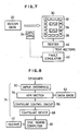
- test vectors 44 there are available product test data (test vectors 44) created by an arbitrary method from arbitrary stage design data, for example created by a simulation engine, a fault simulator, and a test vector generator, etc. , for example. More specifically, since a circuit where any trouble has been arbitrarily produced can be implemented into an actual machine (30) as shown in Fig. 10, operation time of test vectors in units of seconds or minutes can be estimated in real time.
- an output pattern 48 of a device tested using an input pattern (DUT input pattern) 46 can also be prepared very rapidly in real time.
- a first embodiment of a programmable one-board computer comprises, as illustrated in Fig. 1, a system board 32 including wiring (not shown), a single microprocessor (CPU) chip 34 disposed substantially at the centre of the system board 32, and a plurality of (12 in the figure) programmable logic devices (PLD) 36 disposed to substantially surround the circumference of the microprocessor chip 34.
- a system board 32 including wiring (not shown), a single microprocessor (CPU) chip 34 disposed substantially at the centre of the system board 32, and a plurality of (12 in the figure) programmable logic devices (PLD) 36 disposed to substantially surround the circumference of the microprocessor chip 34.
- PLD programmable logic devices
- the embodiment can accept a versatile system by defining the memory while matching it with such a system using an external development tool. Additionally, the embodiment can accept such a system rapidly and easily by also rewriting the memory when the system is altered.
- the PLD since the PLD includes the memory for defining the internal circuit thereof, no external memory device is required in the system board 32, allowing very simple construction and flexibility.
- the number of PLDs 36 is increased, eg doubled, to surround the CPU chip 34, and external memory devices for defining the internal circuits of the PLDs, PROMs 38 for example, instead of beings part of the PLDs, are disposed in the four corners in the present embodiment.
- the present embodiment can provide a versatile system by defining the internal circuit of the PLD by the PROM 38.
- the third embodiment comprises a system board 32 and a CPU chip 34 similar to those in the first embodiment, a plurality of (8 in the present case) large scale programmable logic devices (PLD) 36A disposed to substantially surround the circumference of the CPU chip 34, and a plurality of (28 in the present case) small scale PLDs 36B disposed outside the large scale PLDs 36A.
- PLD programmable logic devices
- the present embodiment facilitates, as illustrated in Fig. 4 for example, circuit definition of a construction that corresponds to large and small size PLDs connected in a hierarchy (hierarchical) structure, the so-called hierarchy design.
- this includes a structure large-sized circuit such as a co-processor circuit which is directly coupled to a CPU and receives from and delivers to the CPU at a high speed for executing partial data processing jointly with the CPU.
- the circuit may therefore be defined within the large scale PLD 36A.
- the large scale PLD 36A is located in the vicinity of the CPU chip 34 so that the embodiment is capable of high speed operation with high efficiency and is preferable for a hierarchy structure system.
- a plurality of CPU chips (three of 34A, 34B, and 34C in the figure) by changing makers and a bit number such as 8, 16, and 32 bits, etc., for example.
- makers and a bit number of the CPU chip are selectable in proper conformity with the system, allowing a board size to be increased but improving flexibility of the embodiment.
- microprocessor chips 34, 34A, 34B, and 34C there were used those including memories and I/O circuits, etc., which are commercially available, a microprocessor chip may also be used which only includes a centre core without such memories and I/O circuits, etc.
- the circumferential PLDs can be available for memories and I/O circuits, etc., included in a typical microprocessor. This case is therefore advantageous particularly to the development of CPUs.
- peripheral circuits of the microprocessor that are difficult to be constructed as PLDs, such as A/D converter, D/A converter, DC/DC converter, ELD (Electronic Luminescence Display) driver, power failure detection circuit, multiplier, FFT processor, and cash (cache) tag memory
- PLDs 36, 36A, and 36B those including a computer system memory may be useable. This situation assures fast access and hence high speed operation, because the PLD includes there in a computer system memory. It is of course possible to provide external computer system memories such as DRAMs and ROMs on the system board 32 independently of the PLDs.
- a designed logic circuit (design data) 20 is altered to a programmable logic device (PLD) circuit using a development tool 24 which is then realized as an actual verification circuit including a PLD, e.g., a programmable one-board computer 30 that includes at least one (two in the figure) microprocessor (CPU) chip 34 disposed substantially at the centre of the system board 32 and a plurality of the PLDs 36 disposed to substantially surround the circumference of the CPU chip 34.
- PLD programmable logic device
- the circuit realized as the verification circuit (30) is used for verification of the function and timing, etc., of the logic circuit 20 through a tester 42 into which a test vector is inputted from a fault simulator 40.
- the development tool 24 comprises an input interface unit 50 into which a logic circuit designed by a designer is inputted, a data base 52 in which there is stored much alteration data of combinations of conventional partial circuits which have already been designed and PLD actual circuits, an APR (Automatic Placement Router) section 54 for altering a logic circuit inputted from the input interface unit 50 to actual circuits of PLDs based upon the data stored in the data base 52, and a configuration control circuit 56 and a configuration device 58 for realizing the circuit altered by the APR section 54 as an actual verification circuit including PLDs, the aforementioned programmable one-board computer 30, for example.
- APR Automatic Placement Router
- a large volume of data is stored in the form of libraries as design property for each corresponding partial circuit, such data including combinations of: designs of prior partial (peripheral) circuits in respective design steps: for example, a logical design level including block diagrams, flow charts, state transition tables, and state transition maps, etc., a hardware description language (HDL) level including function description expressed by definition formulae including a code representative of the current status and a code representative of the next status, and a schematic level including a schematic diagram expressed by symbols, and of: data on transistor level PLD circuits obtained by realizing the aforementioned designs of the prior partial circuits, the combinations of designs of prior partial circuits and of data about transistor level PLD circuits, consisting e.g. of which microprocessor is used and how many microprocessors are used, what peripheral chips (memory, TTL, PLD, and the like) are used and how many peripheral chips are used, and how they are wired and connected, and so on.
- a logical design level including block diagrams, flow charts,
- the calculating section 54 selectively takes out from the data base 52 actual circuits Da, ... corresponding to the partial circuits A, B, C, D and E obtained by dividing up input logic circuit 20 and lays them out on the PLDs in the one-board computer 30, to determine the arrangement and wiring of the logic circuit, as illustrated in Fig. 6.
- logical design level data for example may sometimes be difficult to alter directly to an actual circuit.
- the data maybe lowered once to the HDL level which may then be altered to an actual circuit.
- a test signal is inputted into the verification circuit realized on the programmable one-board computer 30 through the tester 42, whereby real time verification work is achieved with use of the actual circuit.
- failure data circuits which are obtained by intentionally producing internal failures such as bad elements and disconnections, are employed instead of the design data to realize the failure circuit on the one-board computer 30, into which the test vector is inputted to estimate rapidly in real time the fault detection rate, etc., of the test vector, as illustrated in Fig. 10.
- the test pattern is inputted into a verification circuit realized on the one-board computer 30 to obtain rapidly in real time a corresponding output pattern, as illustrated in Fig. 11. Therefore, any combination of such input and output patterns can be obtained with ease.
- the logic circuit 20 is realized as a verification circuit for verification of an actual circuit so that the verification is achievable in real time, much more quickly than computation to ensure rapid verification work.
- use of an actual circuit sharply reduces the possibility of any mistakes.
- use of a programmable logic device circuit facilitates alteration of a designed logic circuit to an actual circuit.
- Use of the programmable one-board computer 30 as a device for realization of an actual circuit ensures realization of an arbitrary actual circuit with ease.
- the PLD 36 for example includes therein a memory (SRAM or EPROM, for example) for defining an internal circuit thereof, whose memory is then defined after an associated system using the development tool 24.
- the programmable one-board computer can accept a versatile system. Further, even if the system is changed, the programmable one-board computer can accept such a change rapidly and easily by rewriting the above memory.
- the memory for defining an internal circuit of a PLD is included in the PLD, so that the need to provide external memory devices in the system board 32 is eliminated, resulting in a very simple and flexible construction.
- a one-board computer 30 composed of two CPU chips and many PLDs, and makers (types) for those CPU chips and a bit number of the same are selectable as required to emulate an associated system, resulting in very high flexibility of the device, although there no limitation to the types of one-board computers for realizing any actual circuit.
- the number of the PLDs 36 may be further increased around the CPU 34, e.g. doubled, and external memories for defining the internal circuit of the PLD 36, (e.g., the PROMs 38) instead of being part of the PLDs may be disposed in the four corners of the board.
- external memories for defining the internal circuit of the PLD 36, (e.g., the PROMs 38) instead of being part of the PLDs may be disposed in the four corners of the board.
- PLDs programmable logic devices
- a programmable one-board computer (3) comprising a system board (32) including wiring, one or more microprocessor chips (34) disposed at the centre of the system board, and a plurality of programmable logic devices (PLDs) (36) disposed to surround the microprocessor chip(s).
- PLDs programmable logic devices
- Each PLD may include a memory (38) for defining an internal circuit thereof or may substitute partly for an external memory device.
- the PLDs may comprise large scale PLDs (36A) as inner PLDs and small scale PLDs (36B) as outer PLDs.
- the programmable one-board computer (30) can realize an actual circuit altered from a newly designed logic circuit (20) and laid out on the same. The actual circuit can be used for verification.
- the programmable one-board computer is capable of accepting varieties of systems and of accepting alterations of those systems quickly and easily by making use of a programmable logic device (PLD), the internal circuit of which is erasable/reconfigurable.
- PLD programmable logic device
Landscapes
- Engineering & Computer Science (AREA)
- Computer Hardware Design (AREA)
- Theoretical Computer Science (AREA)
- Physics & Mathematics (AREA)
- General Engineering & Computer Science (AREA)
- General Physics & Mathematics (AREA)
- Evolutionary Computation (AREA)
- Geometry (AREA)
- Software Systems (AREA)
- Tests Of Electronic Circuits (AREA)
- Design And Manufacture Of Integrated Circuits (AREA)
Applications Claiming Priority (6)
| Application Number | Priority Date | Filing Date | Title |
|---|---|---|---|
| JP1110493A JPH02287604A (ja) | 1989-04-27 | 1989-04-27 | プログラマブルワンボードコンピユータ |
| JP110493/89 | 1989-04-27 | ||
| JP112587/89 | 1989-05-01 | ||
| JP1112587A JPH02291980A (ja) | 1989-05-01 | 1989-05-01 | 論理回路の検証方法 |
| JP112588/89 | 1989-05-01 | ||
| JP1112588A JPH02291080A (ja) | 1989-05-01 | 1989-05-01 | 論理回路の実回路変換方法 |
Publications (2)
| Publication Number | Publication Date |
|---|---|
| EP0403061A2 true EP0403061A2 (fr) | 1990-12-19 |
| EP0403061A3 EP0403061A3 (fr) | 1991-12-27 |
Family
ID=27311749
Family Applications (1)
| Application Number | Title | Priority Date | Filing Date |
|---|---|---|---|
| EP19900304570 Withdrawn EP0403061A3 (fr) | 1989-04-27 | 1990-04-26 | Ordinateur sur plaque unique incorporant les dispositifs à logique programmable et son utilisation pour l'exécution et la vérification automatique de circuit de logique |
Country Status (4)
| Country | Link |
|---|---|
| US (1) | US5253181A (fr) |
| EP (1) | EP0403061A3 (fr) |
| KR (1) | KR900016862A (fr) |
| CA (1) | CA2015421A1 (fr) |
Cited By (1)
| Publication number | Priority date | Publication date | Assignee | Title |
|---|---|---|---|---|
| FR2752967A1 (fr) * | 1996-09-03 | 1998-03-06 | Info Technologies | Procede de developpement d'un circuit integre specifique d'une application (asic) et emulateur correspondant |
Families Citing this family (35)
| Publication number | Priority date | Publication date | Assignee | Title |
|---|---|---|---|---|
| US5644497A (en) * | 1988-03-15 | 1997-07-01 | Hyman; Edward | Method and apparatus for compiling and implementing state-machine states and outputs for a universal cellular sequential logic array |
| US5452231A (en) * | 1988-10-05 | 1995-09-19 | Quickturn Design Systems, Inc. | Hierarchically connected reconfigurable logic assembly |
| US5377124A (en) * | 1989-09-20 | 1994-12-27 | Aptix Corporation | Field programmable printed circuit board |
| DE69133311T2 (de) * | 1990-10-15 | 2004-06-24 | Aptix Corp., San Jose | Verbindungssubstrat mit integrierter Schaltung zur programmierbaren Verbindung und Probenuntersuchung |
| WO1993016433A1 (fr) * | 1992-02-07 | 1993-08-19 | Seiko Epson Corporation | Procede et accelerateur concernant l'emulation de materiels informatiques |
| US5629876A (en) * | 1992-07-10 | 1997-05-13 | Lsi Logic Corporation | Method and apparatus for interim in-situ testing of an electronic system with an inchoate ASIC |
| US5339262A (en) * | 1992-07-10 | 1994-08-16 | Lsi Logic Corporation | Method and apparatus for interim, in-situ testing of an electronic system with an inchoate ASIC |
| US5432708A (en) * | 1992-10-08 | 1995-07-11 | Aptix Corporation | Multichip module integrated circuit device having maximum input/output capability |
| JPH06125067A (ja) * | 1992-10-12 | 1994-05-06 | Mitsubishi Electric Corp | 半導体集積回路及びその設計方法 |
| JPH06236367A (ja) * | 1992-11-12 | 1994-08-23 | Ricoh Co Ltd | 文書作成装置の制御方法 |
| JPH0721229A (ja) * | 1993-06-24 | 1995-01-24 | Fujitsu Ltd | 分配系付加回路自動発生処理方式 |
| US6067615A (en) * | 1993-11-30 | 2000-05-23 | Trw Inc. | Reconfigurable processor for executing successive function sequences in a processor operation |
| US5633813A (en) * | 1994-05-04 | 1997-05-27 | Srinivasan; Seshan R. | Apparatus and method for automatic test generation and fault simulation of electronic circuits, based on programmable logic circuits |
| JP3168839B2 (ja) * | 1994-09-09 | 2001-05-21 | 株式会社日立製作所 | 論理エミュレーションシステム及び等価回路生成方法 |
| US7844517B2 (en) | 1996-01-18 | 2010-11-30 | Planalytics, Inc. | System, method, and computer program product for forecasting weather-based demand using proxy data |
| US7069232B1 (en) | 1996-01-18 | 2006-06-27 | Planalytics, Inc. | System, method and computer program product for short-range weather adapted, business forecasting |
| US6584447B1 (en) | 1996-01-18 | 2003-06-24 | Planalytics, Inc. | Method and computer program product for weather adapted, consumer event planning |
| JPH09231130A (ja) * | 1996-02-26 | 1997-09-05 | Mitsubishi Electric Corp | マイクロコンピュータ |
| US6321366B1 (en) | 1997-05-02 | 2001-11-20 | Axis Systems, Inc. | Timing-insensitive glitch-free logic system and method |
| US6009256A (en) * | 1997-05-02 | 1999-12-28 | Axis Systems, Inc. | Simulation/emulation system and method |
| US6389379B1 (en) | 1997-05-02 | 2002-05-14 | Axis Systems, Inc. | Converification system and method |
| US6134516A (en) * | 1997-05-02 | 2000-10-17 | Axis Systems, Inc. | Simulation server system and method |
| US6421251B1 (en) | 1997-05-02 | 2002-07-16 | Axis Systems Inc | Array board interconnect system and method |
| US6026230A (en) * | 1997-05-02 | 2000-02-15 | Axis Systems, Inc. | Memory simulation system and method |
| US6145020A (en) * | 1998-05-14 | 2000-11-07 | Advanced Technology Materials, Inc. | Microcontroller incorporating an enhanced peripheral controller for automatic updating the configuration date of multiple peripherals by using a ferroelectric memory array |
| US6418417B1 (en) * | 1998-10-08 | 2002-07-09 | Strategic Weather Services | System, method, and computer program product for valuating weather-based financial instruments |
| JP3825572B2 (ja) * | 1999-01-18 | 2006-09-27 | 株式会社東芝 | 半導体集積回路の設計検証装置、方法及び記憶媒体 |
| US7080018B1 (en) | 1999-05-10 | 2006-07-18 | Planalytics, Inc. | Method for weather-based advertising |
| JP2001060210A (ja) * | 1999-08-20 | 2001-03-06 | Nec Corp | Lsi検証方法、lsi検証装置および記録媒体 |
| US7031927B1 (en) | 2000-04-12 | 2006-04-18 | Strategic Weather Services | System, method, and computer program product for weather and terrestrial vegetation-based water renovation and management forecasting |
| US7184965B2 (en) * | 2003-10-29 | 2007-02-27 | Planalytics, Inc. | Systems and methods for recommending business decisions utilizing weather driven demand data and opportunity and confidence measures |
| US7752106B1 (en) | 2005-07-19 | 2010-07-06 | Planalytics, Inc. | System, method, and computer program product for predicting a weather-based financial index value |
| US7360137B2 (en) * | 2006-05-04 | 2008-04-15 | Westell Technologies, Inc. | Flash programmer for programming NAND flash and NOR/NAND combined flash |
| US20070258298A1 (en) * | 2006-05-04 | 2007-11-08 | Westell Technologies, Inc. | Parallel programming of flash memory during in-circuit test |
| US20100287571A1 (en) * | 2009-05-07 | 2010-11-11 | Cypress Semiconductor Corporation | Development, programming, and debugging environment |
Family Cites Families (14)
| Publication number | Priority date | Publication date | Assignee | Title |
|---|---|---|---|---|
| JPS53132245A (en) * | 1977-04-25 | 1978-11-17 | Hitachi Ltd | Subminiature computer |
| JPS59154055A (ja) * | 1983-02-22 | 1984-09-03 | Hitachi Ltd | 論理回路基板上の素子配置方法 |
| US4590581A (en) * | 1983-05-09 | 1986-05-20 | Valid Logic Systems, Inc. | Method and apparatus for modeling systems of complex circuits |
| US4635218A (en) * | 1983-05-09 | 1987-01-06 | Valid Logic Systems | Method for simulating system operation of static and dynamic circuit devices |
| JPS6124250A (ja) * | 1984-07-13 | 1986-02-01 | Nippon Gakki Seizo Kk | 半導体集積回路装置 |
| NL193475C (nl) * | 1984-12-27 | 1999-11-02 | Sony Corp | Microprocessorinrichting. |
| US4744084A (en) * | 1986-02-27 | 1988-05-10 | Mentor Graphics Corporation | Hardware modeling system and method for simulating portions of electrical circuits |
| DE3785084D1 (de) * | 1986-06-06 | 1993-05-06 | Siemens Ag | Verfahren zur simulation eines unterbrechungsfehlers in einer logikschaltung mit feldeffekttransistoren und anordnungen zur durchfuehrung des verfahrens. |
| JPH07120359B2 (ja) * | 1986-10-21 | 1995-12-20 | 日本電気株式会社 | ハードウェアシミュレータにおけるシミュレーション方法 |
| JP2699377B2 (ja) * | 1987-02-25 | 1998-01-19 | 日本電気株式会社 | ハードウエア論理シミユレータ |
| US4852016A (en) * | 1987-06-26 | 1989-07-25 | Seattle Silicon Corporation | Moat router for integrated circuits |
| US4947357A (en) * | 1988-02-24 | 1990-08-07 | Stellar Computer, Inc. | Scan testing a digital system using scan chains in integrated circuits |
| US4931946A (en) * | 1988-03-10 | 1990-06-05 | Cirrus Logic, Inc. | Programmable tiles |
| US5155692A (en) * | 1989-08-21 | 1992-10-13 | At&T Bell Laboratories | Technique for routing conductive paths |
-
1990
- 1990-04-24 US US07/513,625 patent/US5253181A/en not_active Expired - Lifetime
- 1990-04-25 CA CA002015421A patent/CA2015421A1/fr not_active Abandoned
- 1990-04-26 EP EP19900304570 patent/EP0403061A3/fr not_active Withdrawn
- 1990-04-27 KR KR1019900005965A patent/KR900016862A/ko not_active Withdrawn
Cited By (2)
| Publication number | Priority date | Publication date | Assignee | Title |
|---|---|---|---|---|
| FR2752967A1 (fr) * | 1996-09-03 | 1998-03-06 | Info Technologies | Procede de developpement d'un circuit integre specifique d'une application (asic) et emulateur correspondant |
| EP0831408A1 (fr) * | 1996-09-03 | 1998-03-25 | Info technologies | Procédé de développement d'un circuit intégré spécifique d'une application (ASIC) et émulateur correspondant |
Also Published As
| Publication number | Publication date |
|---|---|
| KR900016862A (ko) | 1990-11-14 |
| US5253181A (en) | 1993-10-12 |
| CA2015421A1 (fr) | 1990-10-27 |
| EP0403061A3 (fr) | 1991-12-27 |
Similar Documents
| Publication | Publication Date | Title |
|---|---|---|
| EP0403061A2 (fr) | Ordinateur sur plaque unique incorporant les dispositifs à logique programmable et son utilisation pour l'exécution et la vérification automatique de circuit de logique | |
| Wang et al. | Electronic design automation: synthesis, verification, and test | |
| US7089517B2 (en) | Method for design validation of complex IC | |
| US5812414A (en) | Method for performing simulation using a hardware logic emulation system | |
| US6083269A (en) | Digital integrated circuit design system and methodology with hardware | |
| US5339262A (en) | Method and apparatus for interim, in-situ testing of an electronic system with an inchoate ASIC | |
| US7340700B2 (en) | Method for abstraction of manufacturing test access and control ports to support automated RTL manufacturing test insertion flow for reusable modules | |
| US5036473A (en) | Method of using electronically reconfigurable logic circuits | |
| US5581742A (en) | Apparatus and method for emulating a microelectronic device by interconnecting and running test vectors on physically implemented functional modules | |
| US20080313513A1 (en) | Method and Apparatus for Synthesis of Multimode X-Tolerant Compressor | |
| EP0688451A1 (fr) | Circuits integres programmes par masque a compatibilite logique et de synchronisation avec des reseaux logiques a configuration utilisateur | |
| US7065724B2 (en) | Method and apparatus for generating and verifying libraries for ATPG tool | |
| US8010918B2 (en) | Method for creating HDL description files of digital systems, and systems obtained | |
| Sun et al. | Design and implementation of a parity-based BIST scheme for FPGA global interconnects | |
| Pateras et al. | BIST: a test a diagnosis methodology for complex, high reliability electronics systems | |
| Kessler et al. | An introduction to standard-cell VLSI design: Very large scale integration (VLSI) is becoming an important means of producing electronic circuits at low cost, on tight schedules, and with protection for proprietary designs | |
| Falk | Tools II/Design techniques: Design for production: The computer steps in to automate physical design and testing of computers and other electronic equipment | |
| Joe | Incremental Test Pattern Generation for structurally similar circuits | |
| CN121833534A (zh) | 一种rc测试用例的自动化生成方法及装置 | |
| JPH02291980A (ja) | 論理回路の検証方法 | |
| Niggemeyer et al. | Use of a field programmable gate array for education in manufacturing test and automatic test equipment | |
| DesMarais et al. | Fault simulation and digital circuit testability | |
| Chakraborty | New techniques in testing and timing verification of SYSTEM-ON-CHIPS | |
| Broster et al. | The role of CAD in semicustom IC design | |
| Meyer | The one million gate ASIC challenge: not with behavioral modeling and synthesis |
Legal Events
| Date | Code | Title | Description |
|---|---|---|---|
| PUAI | Public reference made under article 153(3) epc to a published international application that has entered the european phase |
Free format text: ORIGINAL CODE: 0009012 |
|
| AK | Designated contracting states |
Kind code of ref document: A2 Designated state(s): DE FR GB NL |
|
| PUAL | Search report despatched |
Free format text: ORIGINAL CODE: 0009013 |
|
| AK | Designated contracting states |
Kind code of ref document: A3 Designated state(s): DE FR GB NL |
|
| 17P | Request for examination filed |
Effective date: 19920227 |
|
| 17Q | First examination report despatched |
Effective date: 19931217 |
|
| STAA | Information on the status of an ep patent application or granted ep patent |
Free format text: STATUS: THE APPLICATION IS DEEMED TO BE WITHDRAWN |
|
| 18D | Application deemed to be withdrawn |
Effective date: 19940428 |