EP0403075A2 - BICMOS-Hochleistungsschaltkreis mit voller Ausgangsspannungsschwingung - Google Patents
BICMOS-Hochleistungsschaltkreis mit voller Ausgangsspannungsschwingung Download PDFInfo
- Publication number
- EP0403075A2 EP0403075A2 EP90305145A EP90305145A EP0403075A2 EP 0403075 A2 EP0403075 A2 EP 0403075A2 EP 90305145 A EP90305145 A EP 90305145A EP 90305145 A EP90305145 A EP 90305145A EP 0403075 A2 EP0403075 A2 EP 0403075A2
- Authority
- EP
- European Patent Office
- Prior art keywords
- transistor
- circuit
- output
- pull
- transistors
- Prior art date
- Legal status (The legal status is an assumption and is not a legal conclusion. Google has not performed a legal analysis and makes no representation as to the accuracy of the status listed.)
- Granted
Links
Images







Classifications
-
- H—ELECTRICITY
- H03—ELECTRONIC CIRCUITRY
- H03K—PULSE TECHNIQUE
- H03K19/00—Logic circuits, i.e. having at least two inputs acting on one output; Inverting circuits
- H03K19/02—Logic circuits, i.e. having at least two inputs acting on one output; Inverting circuits using specified components
- H03K19/08—Logic circuits, i.e. having at least two inputs acting on one output; Inverting circuits using specified components using semiconductor devices
- H03K19/094—Logic circuits, i.e. having at least two inputs acting on one output; Inverting circuits using specified components using semiconductor devices using field-effect transistors
- H03K19/0944—Logic circuits, i.e. having at least two inputs acting on one output; Inverting circuits using specified components using semiconductor devices using field-effect transistors using MOSFET or insulated gate field-effect transistors, i.e. IGFET
- H03K19/09448—Logic circuits, i.e. having at least two inputs acting on one output; Inverting circuits using specified components using semiconductor devices using field-effect transistors using MOSFET or insulated gate field-effect transistors, i.e. IGFET in combination with bipolar transistors [BIMOS]
-
- H—ELECTRICITY
- H03—ELECTRONIC CIRCUITRY
- H03K—PULSE TECHNIQUE
- H03K19/00—Logic circuits, i.e. having at least two inputs acting on one output; Inverting circuits
- H03K19/02—Logic circuits, i.e. having at least two inputs acting on one output; Inverting circuits using specified components
- H03K19/08—Logic circuits, i.e. having at least two inputs acting on one output; Inverting circuits using specified components using semiconductor devices
-
- H—ELECTRICITY
- H03—ELECTRONIC CIRCUITRY
- H03K—PULSE TECHNIQUE
- H03K19/00—Logic circuits, i.e. having at least two inputs acting on one output; Inverting circuits
- H03K19/0008—Arrangements for reducing power consumption
Definitions
- a logic circuit which operates at a relatively fast speed under a wide range of loading conditions in comparison with prior art circuits performing the same logic operation.
- the logic circuit is capable of providing a virtually full output voltage swing. Furthermore, the logic circuit dissipates practically no static power.
- the invention provides a first transistor connected across the terminals of a first pull-up device, at the output of the logic circuit.
- the first pull up device is operable to bring the circuit output to a first predetermined voltage value.
- the first transistor is also connected to a second pull-up device which is operable together with the first transistor to bring the output of the circuit to a second predetermined voltage value in connection with the output reaching the first predetermined voltage value .
- the first transistor shuts off the first pull-up device once the output of the circuit reaches the second predetermined voltage value.
- the output of the circuit is also connected to a first pull-down device and a second transistor.
- a switch is provided in order to allow the output to turn on the first pull-down device such that the output is brought to a third predetermined voltage value and to allow the second transistor to bring the output to a fourth predetermined voltage value .
- the elements are further specified as follows.
- the first pull-up device and the first pull-down device comprise bipolar transistors.
- the second pull-up device comprises at least one field effect transistor.
- the first and second transistors comprise field effect transistors.
- the switch comprises at least one field effect transistor.
- a second pull-down device is connected to the first transistor. The second pull-down device is operable to discharge, in combination with the first transistor, a terminal of the first pull-up device.
- a second preferred embodiment of the invention is the same as the first preferred embodiment of the invention with the exception that the second pull-down device is not included due to the fact that the first transistor is large enough so as not to require the voltage pull-down effort of the second pull-down device.
- a third preferred embodiment of the invention is the same as the first embodiment of the invention with the addition of an inverter connected to and between the gate of the first transistor and the circuit output.
- the gates of the first and second transistor are connected together and to one terminal of the inverter.
- a fourth preferred embodiment of the invention is the same as the third preferred embodiment of the invention with the exception that gates of the first and second transistor are connected to separate voltage supply sources.
- a fifth preferred embodiment of the invention is the same as the third preferred embodiment of the invention with the exception that the first transistor is connected to and between the collector and emitter terminals of the bipolar transistor of the first pull-up device.
- a sixth preferred embodiment of the invention is the same as the fifth preferred embodiment of the invention with the exception that the gates of the first and second transistors are connected to separate power supply sources.
- Figure 1 illustrates a schematic drawing of a first preferred embodiment of the invention.
- a NAND gate logic circuit generally designated by numeral 2
- a first pull-up device comprising n-type bipolar transistor Q1 is coupled to output OUT.
- a second pull-up device comprising p-channel transistors P1 and P2 are connected to the base of transistor Q1 by their drains.
- the sources of transistors P1 and P2 as well as the collector of transistor Q1 is connected to supply voltage Vcc.
- P-channel transistor PB is connected to and between the base and emitter of transistor Q1 with its gate connected to voltage Vee.
- a switch can be substituted for transistor PB with its operation controlled by output OUT.
- this switch may comprise a MOS transistor, a n-channel transistor, a p-channel transistor, a plurality of n-channel and/or p-channel transistors, a bipolar transistor or a plurality of bipolar transistors or a combination of the above.
- Vee throughout the description of the invention represents circuit ground. However, other values for Vee are contemplated and are possible.
- N-channel transistor NB and a first pull-down device comprising n-type bipolar transistor Q2 are coupled to the output of circuit 2.
- a switch comprising n-channel transistors N1B and N2B connected together are connected between circuit output 2 and transistors NB and Q2.
- N-channel transistors N1 and N2 are connected between the circuit inputs at IN1 and IN2 and are coupled to the transistors of the first and second pull-up devices.
- Figure 2 illustrates the on and off states of the transistors in figure 1 in response to logical high or low inputs corresponding to 1 or 0 respectively at inputs IN1 and IN2.
- a plus sign directly after OFF in figure 2 indicates that a transistor is off initially and will eventually turn on at steady state.
- a minus sign directly after ON indicates that a transistor is initially on and will eventually turn off at steady state.
- transistors N1B and N2B are on to provide base current from output OUT to transistor Q2.
- Transistor Q2 will pull the output down to VBE.
- transistors N1, N2 and PB will discharge the base of transistor Q1 to turn transistor Q1 off.
- Transistors N1B, N2B and NB will pull output OUT all the way down to ground and turn transistor Q2 off.
- FIGs 3 and 4 illustrate voltage vs. time plots for various inputs to a computer simulation of the circuit shown schematically in figure 1.
- Most of the through current (defined as the current from Vcc to circuit ground, which, as stated previously in all the drawings pertaining to the invention, is shown as voltage Vee, although voltages other than circuit ground may be used for Vee) between bipolar transistors Q1 and Q2 occur at the output falling edge.
- Through current is synonymous with leakage current.
- This Q1,Q2 through current is due to the relatively slow turn off of transistor Q1.
- the placement of transistor PB between the base and emitter of transistor Q1 helps drain transistor Q1's base charge through transistor Q2 and the paths through transistors N2B and N1B initially.
- Transistors N1 and N2 will continue to drain the remaining base charge when the output falls below the threshold voltage of transistor PB.
- the larger transistor PB is in size, the faster transistor Q1 will turn off.
- a larger transistor PB will decrease transistor Q1's base current and thus slow down output OUT's charging time.
- Transistor Q2, which is turned on during the output falling edge, plays an important role in draining transistor Q1's base charge through transistor PB.
- Transistor NB is intentionally made small in order to increase the base current to transistor Q2. Thus, the discharge path through transistors N2B, N1B and NB is not a very significant one.
- Transistors N1 and N2 need not be large since they discharge the remaining charge in the base of transistor Q1 and make sure Q1 is off.
- Transistor Q1's base voltage should be kept falling as fast as output OUT's voltage in order to prevent transistor Q1 from turning on during a falling edge of output OUT, as shown in figure 3.
- Transistor PB in effect, keeps the base and emitter voltages of transistor Q1 close so that transistor Q1 will not be turned on during the time output OUT is being pulled down in voltage. In the output rising case, as shown in Figure 4, the base of transistor Q1 and output OUT's voltages are initially very close to ground potential. Transistor PB will not turn on until the base of Q1 is charged up, thereby allowing more current to flow into the base of Q1 instead of to output OUT.
- transistor PB Once transistor PB is on, transistor Q1's emitter current will be weakened due to the reduced base current. The rate of the rising voltage at output OUT will be slowed. The point where the slowing down effect occurs can be adjusted by sizing transistor PB as discussed above.
- the size of transistor PB for different types of functions eg. NAND vs. NOR
- the transistor P1 or transistor P2 to transistor PB ratio as well as bipolar sizing are important parameters to determine the overall performance of the logic circuit. Tradeoffs can be made between the transistor sizes of N1 or N2 and PB. The sizes of transistors N1 and N2 can be increased to drain the base charge of transistor Q1 better.
- the size of transistor PB can be reduced.
- the circuit in figure 1 is constructed in such a way that input IN1's signal arrives late.
- the voltage input IN2 should settle before the voltage at IN1 in order to give maximum performance for the circuit.
- input IN1 is connected to the n-channel transistors which are closest to the bipolar bases. This configuration places input IN1 just one n-channel transistor away from discharging transistor Q1 or from providing base current to transistor Q2.
- Figure 5 illustrates a plot of rise/fall time vs. fanout for a computer simulation of the circuit of figure 1.
- the dashed line represents the rise time of the output vs. fanout of the circuit, whereas the solid line represents the fall time of the output vs. fanout of the circuit.
- Figure 6a illustrates a plot of delay vs. fanout for the computer simulation mentioned above with respect to figure 5.
- the dashed line shows the rising delay time of the output vs. fanout for the circuit while the solid line shows the falling delay time of the output vs. fanout for the circuit.
- Figure 6b is a chart illustrating the effect of transistor sizing on circuit delay and through current. Note that it is desirable to eliminate or minimize through current since it results in wasted energy.
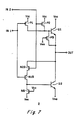
- FIG. 7 is a schematic drawing which illustrates a second preferred embodiment of the invention. This figure is the same as that shown in figure 1 with the exception that transistors N1 and N2 have been removed.
- Figure 8 illustrates the on and off states of the transistors in figure 7 in response to logical high or low inputs corresponding to 1 or 0 respectively at inputs IN1 and IN2.
- a plus sign directly after OFF in figure 7 indicates that a transistor is off initially and will eventually turn on at steady state.
- a minus sign directly after ON indicates that a transistor is initially on and will eventually turn off at steady state.
- Figures 9 and 10 illustrate voltage vs. time plots for various inputs to a computer simulation of the circuit shown schematically in figure 7.
- the operation of the second preferred embodiment of the invention is similar to the first preferred embodiment of the invention.
- the task of turning off transistor Q1 during the output OUT's falling edge is dependent generally on transistor PB alone.
- the effectiveness of transistor PB turning off transistor Q1 decreases as output OUT's voltage drops.
- This second embodiment of the invention is not as immune to noise as the first embodiment of the invention because there is no direct path from the base of transistor Q1 to circuit ground to hold transistor Q1 at an off state.
- this second embodiment of the invention economizes the logic circuit by not requiring at least two transistors in comparison with the first embodiment of the invention.
- Figure 11 illustrates a plot of rise/fall time vs. fanout for a computer simulation of the logic circuit incorporating the second embodiment of the invention.
- the dashed line represents the rise time of the output vs. fanout of the circuit, whereas the solid line represents the fall time of the output vs. fanout of the circuit.
- Figure 12a illustrates a plot of delay vs. fanout for the computer simulation mentioned above with respect to figure 11 .
- the dashed line shows the rising delay time of the output vs. fanout for the circuit while the solid line shows the falling delay time of the output vs. fanout for the circuit.
- Figure 12b is a chart, pertaining to the second embodiment of the invention, which illustrates the effect of transistor sizing on delay and through current.
- FIG. 13 illustrates a schematic drawing of a third embodiment of the invention.
- This embodiment of the invention is the same as the first embodiment of the invention with the exception that inverter 4 has been added and the gates of transistors NB and PB are no longer hardwired to power rails.
- Inverter 4 is connected to add between the gate and drain of transistor PB.
- the gates of transistor NB and PB are connected together.
- Figure 14 illustrates the on and off states of the transistors in figure 13 in response to logical high or low inputs corresponding to 1 or 0 respectively at inputs IN1 and IN2.
- a plus sign directly after OFF in Figure 2 indicates that a transistor is off initially and will eventually turn on at steady state.
- a minus sign directly after ON indicates that a transistor is initially on and will eventually turn off at steady state.
- HL after the inverter output represents a transition from high to low on the inverter output while LH after the inverter output represents a transition from low to high on the inverter output.
- Figures 15 and 16 illustrate voltage vs. time plots for various inputs to a computer simulation of the circuit shown schematically in figure 7.
- this third preferred embodiment of the invention is similar to the first embodiment of the invention.
- operation of of transistors PB and NB are now controlled by inverter 4.
- Inverter 4 can be small in size and is controlled by output OUT. Inverter 4 will not turn transistor PB on until output OUT gets above inverter 4's input threshold voltage. This allows more base current flow into transistor Q1 during output OUT's rising edge. Turning transistor PB on later also moves the knee of the output rising edge in comparison with the second embodiment (see figure 16 and compare with figure 10) to a higher voltage because transistor Q1 has been turned on longer in order to charge up output OUT.
- inverter 4 keeps transistor NB off initially while pulling down output OUT in voltage. This translates into more base current to the base of transistor Q2. Eventually, output OUT drops in voltage below the inverter input threshold voltage. Transistor NB is then turned on and pulls output OUT all the way to circuit ground. Thus rail-to-rail output switching is provided with minimized base current loss due to the level restoring characteristics of transistors PB and NB.
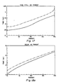
- Figure 17 illustrates a plot of rise/fall time vs. fanout for a computer simulation of the logic circuit incorporating the third embodiment of the invention.
- the dashed line represents the rise time of the output vs. fanout of the circuit, whereas the solid line represents the fall time of the output vs. fanout of the circuit.
- Figure 18a illustrates a plot of delay vs. fanout of the computer simulation mentioned above with respect to figure 17.
- the dashed line shows the rising delay time of the output vs. fanout for the circuit while the solid line shows the falling delay time of the output vs. fanout for the circuit.
- Figure 18b illustrates a chart of transistor sizing and its effect upon circuit delay and through current.
- WIP and WIN represent the sizes of p-channel and n-channel transistors respectively within inverter 4 of figure 13.
- Figure 19 illustrates a schematic drawing of a fourth preferred embodiment of the invention.
- This embodiment of the invention is the same as the third embodiment of the invention with the exception that the source and drain of transistor PB is connected to and between Vcc and output OUT.
- This embodiment of the invention may be faster than the third embodiment of the invention depending upon the series resistance of transistors P2 plus PB. Additionally, notice that there is now no base current drain away from transistor Q1 through transistor PB while charging output OUT through Q1. Unlike that shown in figure 16 with respect to the third embodiment of the invention, the knee of the output rising waveform occurs at approximately Vcc-Vbe since there is no substantial circuit slow down by transistor PB.
- transistors N1 and N2 need to be sized carefully to turn transistor Q1 off while discharging output OUT to prevent excessive crowbar current.
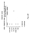
- Figure 20 is a chart which illustrates transistor sizing effects upon circuit delay and through current.
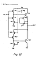
- Figures 21 and 22 are schematic drawings which illustrate fifth and sixth preferred embodiments, respectively, of the invention.
- Figure 21 is the same as figure 19 with the exception that the gate of transistor NB is tied to voltage Vcc.
- Figure 22 is the same as figure 13 with the exception that the gate of transistor NB is likewise tied to voltage Vcc.
- transistor NB will be turned on all of the time.
- a DC (direct current) path between the base of transistor Q2 and Vee (Vee before was indicated as having a value of circuit ground, although other voltages are possible) is established.
- These embodiments do not let the base of transistor Q2 float.
- these embodiments keep the base of transistor Q2 very close to circuit ground rather than Vbe. Therefore the chance of transistor Q2 misfiring when coupling from other activities in the circuit to transistor Q2's base is reduced.
Landscapes
- Engineering & Computer Science (AREA)
- Physics & Mathematics (AREA)
- Computer Hardware Design (AREA)
- Computing Systems (AREA)
- General Engineering & Computer Science (AREA)
- Mathematical Physics (AREA)
- Power Engineering (AREA)
- Logic Circuits (AREA)
Applications Claiming Priority (2)
| Application Number | Priority Date | Filing Date | Title |
|---|---|---|---|
| US35258889A | 1989-05-15 | 1989-05-15 | |
| US352588 | 1989-05-15 |
Publications (3)
| Publication Number | Publication Date |
|---|---|
| EP0403075A2 true EP0403075A2 (de) | 1990-12-19 |
| EP0403075A3 EP0403075A3 (de) | 1991-07-03 |
| EP0403075B1 EP0403075B1 (de) | 1996-04-17 |
Family
ID=23385731
Family Applications (1)
| Application Number | Title | Priority Date | Filing Date |
|---|---|---|---|
| EP90305145A Expired - Lifetime EP0403075B1 (de) | 1989-05-15 | 1990-05-14 | BICMOS-Hochleistungsschaltkreis mit voller Ausgangsspannungsschwingung |
Country Status (4)
| Country | Link |
|---|---|
| EP (1) | EP0403075B1 (de) |
| JP (1) | JPH0394517A (de) |
| KR (1) | KR0157317B1 (de) |
| DE (1) | DE69026534T2 (de) |
Cited By (2)
| Publication number | Priority date | Publication date | Assignee | Title |
|---|---|---|---|---|
| EP0509283A1 (de) * | 1991-04-18 | 1992-10-21 | International Business Machines Corporation | BICMOS Schaltung mit niedriger Schwelle |
| EP0518847A1 (de) * | 1991-05-28 | 1992-12-16 | Austria Mikro Systeme International Aktiengesellschaft | Integrierte Schaltungsanordnung mit Junction-, MOS- und Bipolar-Transistoren |
Families Citing this family (1)
| Publication number | Priority date | Publication date | Assignee | Title |
|---|---|---|---|---|
| KR100872088B1 (ko) * | 2007-06-15 | 2008-12-05 | (주)양지엔지니어링 | 차량용 방호울타리 |
Family Cites Families (8)
| Publication number | Priority date | Publication date | Assignee | Title |
|---|---|---|---|---|
| JPS60125015A (ja) * | 1983-12-12 | 1985-07-04 | Hitachi Ltd | インバ−タ回路 |
| JPH07107973B2 (ja) * | 1984-03-26 | 1995-11-15 | 株式会社日立製作所 | スイツチング回路 |
| US4698526A (en) * | 1985-10-17 | 1987-10-06 | Inmos Corporation | Source follower CMOS input buffer |
| EP0225960B1 (de) * | 1985-12-07 | 1991-03-20 | Deutsche ITT Industries GmbH | CMOS-Inverterkette |
| JPS62221219A (ja) * | 1986-03-22 | 1987-09-29 | Toshiba Corp | 論理回路 |
| JPH0611111B2 (ja) * | 1987-03-27 | 1994-02-09 | 株式会社東芝 | BiMOS論理回路 |
| DE3878345T2 (de) * | 1987-08-17 | 1993-05-27 | Nippon Electric Co | Bimosschaltung, faehig zum betrieb bei hoher geschwindigkeit mit niedrigem verbrauch. |
| JP2593894B2 (ja) * | 1987-11-16 | 1997-03-26 | 富士通株式会社 | 半導体記憶装置 |
-
1990
- 1990-05-14 EP EP90305145A patent/EP0403075B1/de not_active Expired - Lifetime
- 1990-05-14 KR KR1019900006821A patent/KR0157317B1/ko not_active Expired - Fee Related
- 1990-05-14 DE DE69026534T patent/DE69026534T2/de not_active Expired - Fee Related
- 1990-05-15 JP JP2125285A patent/JPH0394517A/ja active Pending
Cited By (2)
| Publication number | Priority date | Publication date | Assignee | Title |
|---|---|---|---|---|
| EP0509283A1 (de) * | 1991-04-18 | 1992-10-21 | International Business Machines Corporation | BICMOS Schaltung mit niedriger Schwelle |
| EP0518847A1 (de) * | 1991-05-28 | 1992-12-16 | Austria Mikro Systeme International Aktiengesellschaft | Integrierte Schaltungsanordnung mit Junction-, MOS- und Bipolar-Transistoren |
Also Published As
| Publication number | Publication date |
|---|---|
| KR900019382A (ko) | 1990-12-24 |
| KR0157317B1 (ko) | 1999-02-18 |
| EP0403075B1 (de) | 1996-04-17 |
| JPH0394517A (ja) | 1991-04-19 |
| EP0403075A3 (de) | 1991-07-03 |
| DE69026534T2 (de) | 1996-09-12 |
| DE69026534D1 (de) | 1996-05-23 |
Similar Documents
| Publication | Publication Date | Title |
|---|---|---|
| US5381059A (en) | CMOS tristateable buffer | |
| US5568065A (en) | Circuit for connecting a node to a voltage source selected from alternative voltage sources | |
| US4731553A (en) | CMOS output buffer having improved noise characteristics | |
| US4672243A (en) | Zero standby current TTL to CMOS input buffer | |
| JP3093380B2 (ja) | 半導体集積回路における信号出力回路 | |
| US6630844B1 (en) | Supply voltage detection circuit | |
| US6249146B1 (en) | MOS output buffer with overvoltage protection circuitry | |
| US20030011402A1 (en) | Output buffer circuit | |
| US6225824B1 (en) | High speed output buffer for high/low voltage operation | |
| EP0555779B1 (de) | TTL/CMOS-Eingangspuffer mit Unterdrückung von Störimpulsen und mit geringem Energieverbrauch | |
| US5173623A (en) | High performance BiCMOS logic circuits with full output voltage swing up to four predetermined voltage values | |
| US7180331B2 (en) | Voltage tolerant structure for I/O cells | |
| US6236245B1 (en) | Output pre-driver for reducing totem pole current | |
| US5541528A (en) | CMOS buffer circuit having increased speed | |
| EP0403075A2 (de) | BICMOS-Hochleistungsschaltkreis mit voller Ausgangsspannungsschwingung | |
| US5118972A (en) | BiCMOS gate pull-down circuit | |
| EP0840453A2 (de) | Ausgangspuffer | |
| US5446321A (en) | BICMOS tri-state circuit with full output voltage swing | |
| GB2270598A (en) | BiCMOS circuit with negative VBE protection | |
| JP2798602B2 (ja) | 出力インタフェース回路 | |
| US5077492A (en) | Bicmos circuitry having a combination cmos gate and a bipolar transistor | |
| US5619153A (en) | Fast swing-limited pullup circuit | |
| JPH05110419A (ja) | Cmosインバータ回路 | |
| EP0600816A2 (de) | BICMOS logische Schaltung mit niedriger Speisespannung | |
| US6559678B1 (en) | Node predisposition circuit |
Legal Events
| Date | Code | Title | Description |
|---|---|---|---|
| PUAI | Public reference made under article 153(3) epc to a published international application that has entered the european phase |
Free format text: ORIGINAL CODE: 0009012 |
|
| AK | Designated contracting states |
Kind code of ref document: A2 Designated state(s): DE FR GB IT NL |
|
| PUAL | Search report despatched |
Free format text: ORIGINAL CODE: 0009013 |
|
| AK | Designated contracting states |
Kind code of ref document: A3 Designated state(s): DE FR GB IT NL |
|
| 16A | New documents despatched to applicant after publication of the search report | ||
| 17P | Request for examination filed |
Effective date: 19920103 |
|
| 17Q | First examination report despatched |
Effective date: 19940822 |
|
| GRAA | (expected) grant |
Free format text: ORIGINAL CODE: 0009210 |
|
| ITF | It: translation for a ep patent filed | ||
| AK | Designated contracting states |
Kind code of ref document: B1 Designated state(s): DE FR GB IT NL |
|
| PG25 | Lapsed in a contracting state [announced via postgrant information from national office to epo] |
Ref country code: NL Free format text: LAPSE BECAUSE OF FAILURE TO SUBMIT A TRANSLATION OF THE DESCRIPTION OR TO PAY THE FEE WITHIN THE PRESCRIBED TIME-LIMIT Effective date: 19960417 |
|
| REF | Corresponds to: |
Ref document number: 69026534 Country of ref document: DE Date of ref document: 19960523 |
|
| ET | Fr: translation filed | ||
| NLV1 | Nl: lapsed or annulled due to failure to fulfill the requirements of art. 29p and 29m of the patents act | ||
| PLBE | No opposition filed within time limit |
Free format text: ORIGINAL CODE: 0009261 |
|
| STAA | Information on the status of an ep patent application or granted ep patent |
Free format text: STATUS: NO OPPOSITION FILED WITHIN TIME LIMIT |
|
| 26N | No opposition filed | ||
| REG | Reference to a national code |
Ref country code: GB Ref legal event code: IF02 |
|
| PGFP | Annual fee paid to national office [announced via postgrant information from national office to epo] |
Ref country code: DE Payment date: 20070531 Year of fee payment: 18 |
|
| PGFP | Annual fee paid to national office [announced via postgrant information from national office to epo] |
Ref country code: GB Payment date: 20070410 Year of fee payment: 18 |
|
| PGFP | Annual fee paid to national office [announced via postgrant information from national office to epo] |
Ref country code: IT Payment date: 20070628 Year of fee payment: 18 |
|
| PGFP | Annual fee paid to national office [announced via postgrant information from national office to epo] |
Ref country code: FR Payment date: 20070503 Year of fee payment: 18 |
|
| GBPC | Gb: european patent ceased through non-payment of renewal fee |
Effective date: 20080514 |
|
| REG | Reference to a national code |
Ref country code: FR Ref legal event code: ST Effective date: 20090119 |
|
| PG25 | Lapsed in a contracting state [announced via postgrant information from national office to epo] |
Ref country code: DE Free format text: LAPSE BECAUSE OF NON-PAYMENT OF DUE FEES Effective date: 20081202 Ref country code: FR Free format text: LAPSE BECAUSE OF NON-PAYMENT OF DUE FEES Effective date: 20080602 |
|
| PG25 | Lapsed in a contracting state [announced via postgrant information from national office to epo] |
Ref country code: GB Free format text: LAPSE BECAUSE OF NON-PAYMENT OF DUE FEES Effective date: 20080514 |
|
| PG25 | Lapsed in a contracting state [announced via postgrant information from national office to epo] |
Ref country code: IT Free format text: LAPSE BECAUSE OF NON-PAYMENT OF DUE FEES Effective date: 20080514 |