EP0403113A2 - Transistor à effet de champs et procédé pour sa fabrication - Google Patents
Transistor à effet de champs et procédé pour sa fabrication Download PDFInfo
- Publication number
- EP0403113A2 EP0403113A2 EP90305911A EP90305911A EP0403113A2 EP 0403113 A2 EP0403113 A2 EP 0403113A2 EP 90305911 A EP90305911 A EP 90305911A EP 90305911 A EP90305911 A EP 90305911A EP 0403113 A2 EP0403113 A2 EP 0403113A2
- Authority
- EP
- European Patent Office
- Prior art keywords
- layer
- field effect
- wafer
- semiconductor device
- tungsten
- Prior art date
- Legal status (The legal status is an assumption and is not a legal conclusion. Google has not performed a legal analysis and makes no representation as to the accuracy of the status listed.)
- Withdrawn
Links
Images






Classifications
-
- H—ELECTRICITY
- H10—SEMICONDUCTOR DEVICES; ELECTRIC SOLID-STATE DEVICES NOT OTHERWISE PROVIDED FOR
- H10D—INORGANIC ELECTRIC SEMICONDUCTOR DEVICES
- H10D30/00—Field-effect transistors [FET]
- H10D30/60—Insulated-gate field-effect transistors [IGFET]
- H10D30/64—Double-diffused metal-oxide semiconductor [DMOS] FETs
- H10D30/66—Vertical DMOS [VDMOS] FETs
-
- H—ELECTRICITY
- H10—SEMICONDUCTOR DEVICES; ELECTRIC SOLID-STATE DEVICES NOT OTHERWISE PROVIDED FOR
- H10D—INORGANIC ELECTRIC SEMICONDUCTOR DEVICES
- H10D12/00—Bipolar devices controlled by the field effect, e.g. insulated-gate bipolar transistors [IGBT]
- H10D12/01—Manufacture or treatment
- H10D12/031—Manufacture or treatment of IGBTs
- H10D12/032—Manufacture or treatment of IGBTs of vertical IGBTs
-
- H—ELECTRICITY
- H10—SEMICONDUCTOR DEVICES; ELECTRIC SOLID-STATE DEVICES NOT OTHERWISE PROVIDED FOR
- H10D—INORGANIC ELECTRIC SEMICONDUCTOR DEVICES
- H10D30/00—Field-effect transistors [FET]
- H10D30/01—Manufacture or treatment
- H10D30/021—Manufacture or treatment of FETs having insulated gates [IGFET]
- H10D30/028—Manufacture or treatment of FETs having insulated gates [IGFET] of double-diffused metal oxide semiconductor [DMOS] FETs
- H10D30/0291—Manufacture or treatment of FETs having insulated gates [IGFET] of double-diffused metal oxide semiconductor [DMOS] FETs of vertical DMOS [VDMOS] FETs
-
- H—ELECTRICITY
- H10—SEMICONDUCTOR DEVICES; ELECTRIC SOLID-STATE DEVICES NOT OTHERWISE PROVIDED FOR
- H10D—INORGANIC ELECTRIC SEMICONDUCTOR DEVICES
- H10D64/00—Electrodes of devices having potential barriers
- H10D64/01—Manufacture or treatment
- H10D64/013—Manufacture or treatment of electrodes having a conductor capacitively coupled to a semiconductor by an insulator
- H10D64/01302—Manufacture or treatment of electrodes having a conductor capacitively coupled to a semiconductor by an insulator the insulator being formed after the semiconductor body, the semiconductor being silicon
- H10D64/01304—Manufacture or treatment of electrodes having a conductor capacitively coupled to a semiconductor by an insulator the insulator being formed after the semiconductor body, the semiconductor being silicon characterised by the conductor
- H10D64/01306—Manufacture or treatment of electrodes having a conductor capacitively coupled to a semiconductor by an insulator the insulator being formed after the semiconductor body, the semiconductor being silicon characterised by the conductor the conductor comprising a layer of silicon contacting the insulator, e.g. polysilicon
- H10D64/01308—Manufacture or treatment of electrodes having a conductor capacitively coupled to a semiconductor by an insulator the insulator being formed after the semiconductor body, the semiconductor being silicon characterised by the conductor the conductor comprising a layer of silicon contacting the insulator, e.g. polysilicon the conductor further comprising a non-elemental silicon additional conductive layer, e.g. a metal silicide layer formed by the reaction of silicon with an implanted metal
- H10D64/01312—Manufacture or treatment of electrodes having a conductor capacitively coupled to a semiconductor by an insulator the insulator being formed after the semiconductor body, the semiconductor being silicon characterised by the conductor the conductor comprising a layer of silicon contacting the insulator, e.g. polysilicon the conductor further comprising a non-elemental silicon additional conductive layer, e.g. a metal silicide layer formed by the reaction of silicon with an implanted metal the additional layer comprising a metal or metal silicide formed by deposition, i.e. without a silicidation reaction, e.g. sputter deposition
-
- H—ELECTRICITY
- H10—SEMICONDUCTOR DEVICES; ELECTRIC SOLID-STATE DEVICES NOT OTHERWISE PROVIDED FOR
- H10D—INORGANIC ELECTRIC SEMICONDUCTOR DEVICES
- H10D64/00—Electrodes of devices having potential barriers
- H10D64/20—Electrodes characterised by their shapes, relative sizes or dispositions
- H10D64/23—Electrodes carrying the current to be rectified, amplified, oscillated or switched, e.g. sources, drains, anodes or cathodes
- H10D64/251—Source or drain electrodes for field-effect devices
- H10D64/252—Source or drain electrodes for field-effect devices for vertical or pseudo-vertical devices
-
- H—ELECTRICITY
- H10—SEMICONDUCTOR DEVICES; ELECTRIC SOLID-STATE DEVICES NOT OTHERWISE PROVIDED FOR
- H10D—INORGANIC ELECTRIC SEMICONDUCTOR DEVICES
- H10D84/00—Integrated devices formed in or on semiconductor substrates that comprise only semiconducting layers, e.g. on Si wafers or on GaAs-on-Si wafers
- H10D84/01—Manufacture or treatment
- H10D84/0102—Manufacture or treatment of thyristors having built-in components, e.g. thyristor having built-in diode
- H10D84/0105—Manufacture or treatment of thyristors having built-in components, e.g. thyristor having built-in diode the built-in components being field-effect devices
-
- H—ELECTRICITY
- H10—SEMICONDUCTOR DEVICES; ELECTRIC SOLID-STATE DEVICES NOT OTHERWISE PROVIDED FOR
- H10W—GENERIC PACKAGES, INTERCONNECTIONS, CONNECTORS OR OTHER CONSTRUCTIONAL DETAILS OF DEVICES COVERED BY CLASS H10
- H10W20/00—Interconnections in chips, wafers or substrates
- H10W20/40—Interconnections external to wafers or substrates, e.g. back-end-of-line [BEOL] metallisations or vias connecting to gate electrodes
- H10W20/41—Interconnections external to wafers or substrates, e.g. back-end-of-line [BEOL] metallisations or vias connecting to gate electrodes characterised by their conductive parts
- H10W20/44—Conductive materials thereof
- H10W20/4451—Semiconductor materials, e.g. polysilicon
-
- H—ELECTRICITY
- H10—SEMICONDUCTOR DEVICES; ELECTRIC SOLID-STATE DEVICES NOT OTHERWISE PROVIDED FOR
- H10D—INORGANIC ELECTRIC SEMICONDUCTOR DEVICES
- H10D62/00—Semiconductor bodies, or regions thereof, of devices having potential barriers
- H10D62/80—Semiconductor bodies, or regions thereof, of devices having potential barriers characterised by the materials
- H10D62/83—Semiconductor bodies, or regions thereof, of devices having potential barriers characterised by the materials being Group IV materials, e.g. B-doped Si or undoped Ge
-
- H—ELECTRICITY
- H10—SEMICONDUCTOR DEVICES; ELECTRIC SOLID-STATE DEVICES NOT OTHERWISE PROVIDED FOR
- H10D—INORGANIC ELECTRIC SEMICONDUCTOR DEVICES
- H10D64/00—Electrodes of devices having potential barriers
- H10D64/60—Electrodes characterised by their materials
- H10D64/62—Electrodes ohmically coupled to a semiconductor
-
- H—ELECTRICITY
- H10—SEMICONDUCTOR DEVICES; ELECTRIC SOLID-STATE DEVICES NOT OTHERWISE PROVIDED FOR
- H10D—INORGANIC ELECTRIC SEMICONDUCTOR DEVICES
- H10D64/00—Electrodes of devices having potential barriers
- H10D64/60—Electrodes characterised by their materials
- H10D64/66—Electrodes having a conductor capacitively coupled to a semiconductor by an insulator, e.g. MIS electrodes
- H10D64/661—Electrodes having a conductor capacitively coupled to a semiconductor by an insulator, e.g. MIS electrodes the conductor comprising a layer of silicon contacting the insulator, e.g. polysilicon having vertical doping variation
- H10D64/662—Electrodes having a conductor capacitively coupled to a semiconductor by an insulator, e.g. MIS electrodes the conductor comprising a layer of silicon contacting the insulator, e.g. polysilicon having vertical doping variation the conductor further comprising additional layers, e.g. multiple silicon layers having different crystal structures
- H10D64/663—Electrodes having a conductor capacitively coupled to a semiconductor by an insulator, e.g. MIS electrodes the conductor comprising a layer of silicon contacting the insulator, e.g. polysilicon having vertical doping variation the conductor further comprising additional layers, e.g. multiple silicon layers having different crystal structures the additional layers comprising a silicide layer contacting the layer of silicon, e.g. polycide gates
Definitions
- This invention relates in general to semiconductor devices and methods for fabricating same.
- the invention relates to power field effect semiconductor device fabrication methods and structures.
- Gate electrodes in vertical power field effect devices are commonly formed by wet etching or dry etching heavily doped polysilicon/oxide stacks prior to channel and source implantation and diffusion.
- the lowest attainable gate sheet resistance using this method is typically 20-25 ohms/square, which is due principally to the solid solubility limitation of the dopant (e.g. phosphorous) within the polysilicon laver.
- the dopant e.g. phosphorous
- FETs high frequency, low voltage power field effect transistors
- a gate sheet resistance of 20-25 ohms/square is high and functions to disadvantageously restrict the gate turn-on and turn-off times and results in increased gate switching losses.
- non-uniform turn-on and turn-off resistance/capacitance (RC) mechanisms often result which significantly hinder the frequency response of such devices and cause local hot spots.
- VLSI very large scale integrated circuits
- V BD 50-100 volts, or less
- Such devices will allow local distribution of power to an integrated circuit.
- gate sheet resistance e.g. to ⁇ 20-25 ohms/square
- Another barrier to obtaining practical high frequency, low voltage power field effect devices is the significant contribution to on-resistance of the device from the source, gate and drain ohmic contacts. To reduce the on-stage power dissipation and to improve the current handling capability of the device, a low specific on-resistance is desired.
- metal silicide is directed to the specific purpose of increasing the conductivity of a particular silicon region in order that the region itself may have a low resistance to the flow of current along the length thereof.
- prior uses of metal silicide have required additional processing steps and/or placed processing limitations on device fabrication. For example, additional masking and etching are typically necessary, and once deposited, high temperature drive must be avoided.
- One aspect of the invention provides a tungsten silicide/polysilicon/oxide electrode stack with low sheet resistance and/or selective low pressure chemical vapor deposited (LPCVD) tungsten layers on a semiconductor wafer to lower ohmic contact resistance.
- LPCVD selective low pressure chemical vapor deposited
- An embodiment of the present invention aims to provide a multi-cellular, field effect power device operating characteristics having reduced gate sheet resistance.
- Another embodiment of the invention aims to provide a multi-cellular, field effect power device fabrication method and structure with improved on-resistance and lowered ohmic contact resistance.
- a still further embodiment aims to provide an improved high frequency, low voltage, multicellular, field effect power device fabrication method and structure.
- a field effect semiconductor structure including a tungsten silicide/polysilicon/oxide gate electrode stack.
- this structure is combined with a layer of tungsten disposed in ohmic contact with the source and gate regions.
- the tungsten layer is self-aligned with respect to an aperture in the gate electrode stack which is disposed over and preferably self-aligned with the body and source regions. If desired, a tungsten layer can also be provided at the device drain.
- the structure is preferably present in each cell of the multi-cellular device.
- These field effect devices may be FETs, insulated gate bipolar transistors (IGBTs), metal oxide semiconductor controlled thyristors (MCTs) or other field effect power devices in discrete or integrated forms.
- Such a device structure may be fabricated in accordance with one embodiment of the invention by (1) oxidizing the surface of a one type conductivity semiconductor wafer to form an oxide layer, (2) depositing a polysilicon layer on top of the oxide layer, (3) depositing a tungsten silicide layer on top of the polysilicon layer, (4) patterning the tungsten silicide/polysilicon/oxide stack to define a gate electrode layer and an aperture therein, (5) forming a body region of opposite type conductivity in the wafer beneath the self-aligning gate electrode aperture, (6) high-temperature diffusion of the p-type body region with a suitable silicide capping layer such as a thermally grown oxide layer on the silicide, (7) etching the capping layer (preferably dry etch) to allow for source region implant, (8) forming a source region of one type conductivity in the body region beneath the self-aligning gate electrode aperture, and (9) driving the source region diffusions in.
- Further preferred processing steps include (10) growing a thin layer of thermal oxide on the wafer prior to driving the source and body region diffusions, (11) patterning the tungsten silicide/polysilicon/oxide stack using a two step reactive-ion-etching process wherein the silicide layer is etched in a first gas and the balance of the exposed stack is etched in a second gas to define sharp vertical edges, (12) depositing a conformal dielectric layer over the entire upper surface of the wafer, (13) plasma etching the conformal dielectric layer to remove the dielectric layer within the gate layer defined aperture, (14) depositing a layer of tungsten within the window exposed within the gate electrode layer aperture, and (15) depositing a metallization layer over the wafer and in the contact window in a manner to form an ohmic contact between the metallization and the source region within the gate electrode defined aperture.
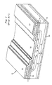
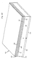
- Figure 1 illustrates in a perspective cross section view, a portion of a prior art field effect power semiconductor device 10.
- the device 10 comprises a body 12 of semiconductor material having upper and lower major surfaces and including an N+ drain layer 14 adjacent its lower surface, and an N- drift region 16 extending from adjacent the drain region 14 to the upper surface of the semiconductor body.
- a body region 18 of P+ material extends into the drift region from the upper surface of the semiconductor body.
- a heavily doped N+ source region 20 extends into the body region 18 from the upper surface of the semiconductor material.
- the source region 20 in the plane of the cut in the figure consists of two separate portions which are locally spaced apart by a portion of the body region 18 which extends to the upper surface of the semiconductor body between the two portions of the source region.
- An insulated gate electrode 31 is disposed on the upper surface of the semiconductor body and comprises a thermal oxide layer 30 and a polysilicon layer 32.
- Oxide layer 30 is approximately 500 ⁇ thick and polysilicon layer 32 is close to 6000 ⁇ thick.
- Layer 32 is POCl3 doped to lower the sheet resistance to approximately 25 ohms/square (which, again, is high for many applications).
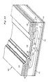
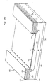
- Device 100 comprises a body 110 of silicon semiconductor material having an upper surface 111 and a lower surface 112. Surfaces 111 and 112 are opposed major surfaces of a wafer and are normally substantially parallel to each other.
- Body 110 comprises an N+ drain region 114 which is disposed adjacent the lower surface 112 of the semiconductor body, and an N-drift region 116 disposed continuous to and above the drain region 114.
- a body region 118 of P type material extends into the drift region from the upper surface 111 of the semiconductor body.
- An N+ source region 120 extends into the body region 118 from upper surface 111 of the semiconductor body.
- Gate electrode 131 is disposed on the upper surface 111 of the semiconductor body.
- Gate electrode 131 comprises an insulating layer 130 (preferably thermal oxide) disposed directly on the upper surface 111 of the semiconductor body and a conductive polycrystalline silicon layer 132 disposed on the oxide layer.
- a tungsten silicide layer 134 is located on the upper surface of polysilicon layer 132.
- Tungsten silicide layer 134 serves to provide the gate electrode with high lateral conductivity. In fact, the lateral conductivity of tungsten silicide layer 134 is sufficiently high that polycrystalline silicon layer 132 itself does not need to be highly conductive.
- Tungsten silicide layer 134 has a further advantage of producing gate sheet resistance values greatly lower than those obtainable with the prior art technique of heavily doping the polysilicon layer.
- the embodiment comprises the disposition of a tungsten layer 136 in contact with source region 120 where it extends to the surface within the aperture defined by the gate electrode.
- Layer 136 serves to improve contact resistance to regions 120 and 118, thereby reducing device on-resistance, improving breakdown voltage, increasing the current handling capability, and optimizing frequency response of the device.
- Tungsten layer 136 is spaced from the gate electrode stack 131 by an interlevel dielectric 138, preferably an oxide layer.
- An overlying source metallization layer 140 makes ohmic contact to tungsten layer 136. Selective gate and source metallization using tungsten can also be performed using a sidewall dielectric spacer structure 140 as shown in Figure 2B.
- IGBT insulated gate bipolar transistors
- MCT metal oxide semiconductor controlled thyristors
- the cells of device 100 are shown and have been described as being parallel, elongated (straight stripe) cells. However, this invention is also applicable to cells of other shapes and configurations, including but not limited to rectangular, including square; hexagonal; round or elliptical, including circular; and so forth.
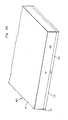
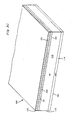
- the device of Figure 2A may be produced in accordance with a novel fabrication process whose steps are illustrated in Figures 3A-3I.
- a semiconductor wafer 110 has an upper surface 111 and a lower surface 112.
- the surfaces 111 and 112 are opposed major surfaces of the wafer 110.
- Adjacent the lower surface 112 is an N+ layer 114 which forms the drain region of the final device.
- the remainder of the wafer in Figure 3A is a lightly doped N type (N-) layer 116 which, in the final device, comprises the drift region of the device.
- N- lightly doped N type
- the upper surface of the wafer has been thermally oxidized in a manner well known in the art to form a 500-1000 angstrom thick thermal oxide layer 130 across the entire upper surface of the wafer 110.
- a substantially uniform layer 132 of polycrystalline silicon has been deposited on top of the oxide layer.
- the polycrystalline silicon may preferably have a thickness of 4000 to 8000 angstroms and may be deposited in any well-known manner, such as by pyrolytic decomposition of silane (SiH4) in a chemical vapor deposition system.
- a tungsten silicide layer 134 is formed on layer 132, preferably by low pressure chemical vapor disposition (LPCVD) (see Figure 3D).
- LPCVD low pressure chemical vapor disposition
- Tungsten silicide layer 134 is approximately 3,000 angstroms thick and is initially deposited with an atomic ratio of silicon to tungsten of approximately 2.6:1. This silicon rich silicide is necessary because a certain amount of silicon will outdiffuse and be lost to the silicide during subsequent high temperature processing of the semiconductor device to form oxide or nitride.
- Tungsten silicide layer 134 is highly conductive, and as deposited is microcrystalline and has a sheet resistance of approximately 14 ohms per square.
- silicide layer 134 allows for easy patterning of the layer.
- Important to the fabrication method of the present embodiment is a two step stack 131 etch process.
- silicide layer 134 is initially patterned and etched away in a first ambient gas to form a window 170 at the bottom of which the upper surface of polysilicon layer 132 is exposed.
- the second etch of the two step process is to remove polysilicon layer 132 and oxide layer 130 in a different ambient gas.
- a second gas is necessary to attain the desired substantially vertical silicide/polysilicon/oxide stack surfaces at the edges of window 170′ (see Figure 3F).
- a number of different etch gas combinations can be used.
- silicide layer 134 can be removed using a SF6 plasma with parameters as follows: flow, 40 sccm; pressure, 50 mTorr; and power, 300 W (0.25 W/cm2).
- One method of etching layers 132 and 130 following reactive-ion-etching of silicide layer 134 in SF6 plasma is to expose the surfaces in an HC1 plasma with etched parameters of: flow, 20 sccm; pressure, 20 mTorr; and power 200 W (0.25 W/cm2).
- the preferred process is obtained using a C12 plasma in the second etch of layers 132 and 130 following selective removal of layer 134 using reactive-ion-etching in CBrF3.
- etchings The parameters for these etchings are: flow, 103 sccm/80 sccm (respectively); pressure, 50 mTorr; and power 300 W (0.25 W/cm2).
- This etch chemistry provides nearly vertical sidewalls with minimal resist erosion.
- Polysilicon sidewalls with controlled etch profiles that are non-reentrant result in improved wafer yield especially for large area power FETs with gate peripheries on the order of several meters.
- a two step dry etch sequence is used to dry clean silicon surface 111 and remove any residual surface damage. Following this, diffusion of a P+ body region 118 through window 170′ is accomplished in the normal manner. Region 118 can be formed by implanting 140 keV, 6 x 10¹³ - 1 x 10¹⁴ boron atoms/cm2 and diffusing at temperatures ranging from 1050° C to 1100° C for varying durations in nitrogen or argon to obtain a range of P base profiles.
- the wafer is first capped with a layer of thermally grown oxide at 950° C prior to high temperature base drives in order to preserve the silicide surface morphology and limit silicon out diffusion from the silicide and polysilicon films.
- the silicide can also be capped by a layer of dielectric deposited at low processing temperatures. Alternatively, the silicide may be annealed by rapid thermal processing.
- the wafer is coated with a layer of photoresist which is patterned to leave a central segment of the photoresist centered in the window 170′, as shown in Figure 3G.
- a heavy concentration of an N type dopant is implanted through the reduced window into the surface of semiconductor body 110.
- the photoresist is stripped from the wafer and the wafer is heated to drive the source region 120 into semiconductor body 110.
- the device at the end of this well-known processing is shown in Figure 3H.
- arsenic implant in place of heretofore known implants, such as phosphorous. Because of defect enhanced diffusion mechanisms, phosphorous generally gives a doping profile that is sharply peaked at the silicon surface and rapidly falls off into the silicon body. For a good ohmic contact, a high doping concentration is required not only at the silicon surface but also for at least a few hundred angstroms deep into the silicon block. It has been discovered that arsenic implants meet this need and, therefore, provide superior source contacts. Further, utilization of arsenic implants does not require any additional process complexities compared to standard phosphorous doped source regions. Implantation of arsenic can be used in all other discrete power devices and high voltage integrated circuit (HVIC) technology, as well as to form good drain ohmic contacts.
- HVIC high voltage integrated circuit
- a 4,000 angstrom thick layer of low temperature oxide is deposited over the wafer at a temperature of about 450° C by low temperature chemical vapor deposition.
- This layer is preferably conformal, but need not be.
- the source gases may preferably be dichlorosilane and nitrous oxide.
- This low temperature oxide layer includes many pinholes. It is therefore densified at a temperature in the 800-900° C range in a nitrogen atmosphere for a period of from 30 to 60 minutes.
- a second 4,000 angstrom thick layer of LTO is deposited on the wafer and densified in a similar manner in order to provide an 8,000 angstrom thick layer 138 ( Figure 3I) of dense, pinhole-free oxide.
- the upper surface of the wafer is coated with a layer of photoresist (not shown) which is patterned to provide a contact hole over the source and body regions 120 and 118.
- the wafer is then reactive-ion-etched in a known manner to expose said source and body regions.
- a layer of silicon oxide forms over the exposed silicon due to a reaction with the oxygen in the air.
- SiO2 silicon oxide
- the oxide in the contact regions must be removed. About 1000 angstroms of LPCVD tungsten is deposited selectively on exposed silicon. The oxide in the contact windows is etched by HF produced in the tungsten deposition system. The deposited tungsten serves several purposes. First, it prevents aluminum spiking which can otherwise result from the subsequent deposition or sintering of an aluminum metallization layer over the wafer. Second, it minimizes contact electromigration of the aluminum metallization.
- An aluminum metallization layer is then sputtered onto the wafer surface, preferably in the same sputtering chamber, but in a different sputtering chamber if desired.
- An aluminum thickness of about 3 microns is preferred.
- the aluminum may be pure aluminum or an aluminum silicon alloy, such as alusil, as is well known in the art.
- the wafer appears as shown in Figure 2A.
- the drain metallization 142 shown in Figure 2A may be applied in the same manner and at the same time as the source metallization.
- the drain metallization is applied after the previously-described passivation on the source side of the wafer has been performed. This may require thinning the wafer, as by grinding, to a thickness of 15-7 mils prior to performing the drain metallization.
- the drain also receives a layer of tungsten metal prior to contact metallization, again to improve ohmic contact resistance.
- Metallization contact to the gate electrode is provided in the usual manner at the periphery of the device active area and is not shown in the figures.
- the wafer is diced into individual devices if multiple devices have been fabricated. Naturally, if a whole wafer device has been fabricated or the fabricated devices are to be used in their wafer form, the wafer is not diced.
- measured room temperature reverse blocking characteristics of 50 V power FETs fabricated pursuant to the above described method show a sharp transition into avalanche breakdown regimen with a drain to source breakdown voltage, V BD , of 45 V.
- V BD drain to source breakdown voltage
- the measured results listed in Table 1 correspond to an optimum cell design for each V BD and were extracted for measurements performed on an average of more than 100 devices distributed across 4 inch diameter silicon wafers.
- the measured R on x C Iss product shown in Table 1 represents the best values reported for any type of power FET in the 50 V and 100 V reverse blocking ranges. More than 40 percent improvement in R on was obtained for package devices when a large number of (for example 50) source bond wires were used to reduce the current crowding effects due to finite resistivity and dimensions of source metallization. The current crowding effect was negligible in smaller dies of 25 mil x 25 mil size.
- the switching times listed in Table 1 were obtained under resistive switching conditions. Accurate measurement of turn-on and turn-off times was difficult when switching large amounts of current due to circuit parasitics. Significant loading of the gate driver circuitry by large input capacitance also added to the complexity. The switching times listed in Table 1 are in reasonable agreement with transient response calculated from a first order circuit model whose parameters were extracted from the measured dc and capacitance results. These devices were able to sustain an avalanche energy of at least 30 mJ when switching energy stored in inductive loads.
Landscapes
- Electrodes Of Semiconductors (AREA)
- Thin Film Transistor (AREA)
Applications Claiming Priority (2)
| Application Number | Priority Date | Filing Date | Title |
|---|---|---|---|
| US07/359,811 US4985740A (en) | 1989-06-01 | 1989-06-01 | Power field effect devices having low gate sheet resistance and low ohmic contact resistance |
| US359811 | 1989-06-01 |
Publications (2)
| Publication Number | Publication Date |
|---|---|
| EP0403113A2 true EP0403113A2 (fr) | 1990-12-19 |
| EP0403113A3 EP0403113A3 (fr) | 1991-03-20 |
Family
ID=23415378
Family Applications (1)
| Application Number | Title | Priority Date | Filing Date |
|---|---|---|---|
| EP19900305911 Withdrawn EP0403113A3 (fr) | 1989-06-01 | 1990-05-31 | Transistor à effet de champs et procédé pour sa fabrication |
Country Status (3)
| Country | Link |
|---|---|
| US (1) | US4985740A (fr) |
| EP (1) | EP0403113A3 (fr) |
| JP (1) | JPH0382043A (fr) |
Families Citing this family (18)
| Publication number | Priority date | Publication date | Assignee | Title |
|---|---|---|---|---|
| US5234851A (en) * | 1989-09-05 | 1993-08-10 | General Electric Company | Small cell, low contact assistance rugged power field effect devices and method of fabrication |
| IT1236994B (it) * | 1989-12-29 | 1993-05-12 | Sgs Thomson Microelectronics | Processo per la fabbricazione di dispositivi semiconduttori mos di potenza e dispositivi con esso ottenuti |
| JP2513055B2 (ja) * | 1990-02-14 | 1996-07-03 | 日本電装株式会社 | 半導体装置の製造方法 |
| JP3144817B2 (ja) * | 1990-03-23 | 2001-03-12 | 株式会社東芝 | 半導体装置 |
| US5413966A (en) * | 1990-12-20 | 1995-05-09 | Lsi Logic Corporation | Shallow trench etch |
| US5354417A (en) * | 1993-10-13 | 1994-10-11 | Applied Materials, Inc. | Etching MoSi2 using SF6, HBr and O2 |
| DE4400032C1 (de) * | 1994-01-03 | 1995-08-31 | Gold Star Electronics | Halbleitereinrichtung und Verfahren zu deren Herstellung |
| DE69434268T2 (de) * | 1994-07-14 | 2006-01-12 | Stmicroelectronics S.R.L., Agrate Brianza | Intergrierte Struktur einer Hochgeschwindigkeits-MOS-Technologe-Leistungsvorrichtung und zugehöriges Herstellungsverfahren |
| US5795793A (en) * | 1994-09-01 | 1998-08-18 | International Rectifier Corporation | Process for manufacture of MOS gated device with reduced mask count |
| EP0785574A3 (fr) | 1996-01-16 | 1998-07-29 | Applied Materials, Inc. | Méthode de fabrication de siliciure de tungstène |
| EP0817274B1 (fr) | 1996-07-05 | 2004-02-11 | STMicroelectronics S.r.l. | Dispositif de puissance en technologie MOS asymétrique |
| DE19840402C2 (de) * | 1997-12-12 | 2003-07-31 | Nat Semiconductor Corp | Verfahren zum Herstellen einer Struktur eines DMOS-Leistungselementes und Struktur eines DMOS-Leistungselementes |
| US6218701B1 (en) | 1999-04-30 | 2001-04-17 | Intersil Corporation | Power MOS device with increased channel width and process for forming same |
| US6211550B1 (en) * | 1999-06-24 | 2001-04-03 | Intersil Corporation | Backmetal drain terminal with low stress and thermal resistance |
| US20040036131A1 (en) * | 2002-08-23 | 2004-02-26 | Micron Technology, Inc. | Electrostatic discharge protection devices having transistors with textured surfaces |
| US6756619B2 (en) * | 2002-08-26 | 2004-06-29 | Micron Technology, Inc. | Semiconductor constructions |
| US10395988B1 (en) | 2018-04-10 | 2019-08-27 | International Business Machines Corporation | Vertical FET transistor with reduced source/drain contact resistance |
| CN111540727B (zh) * | 2020-03-28 | 2023-05-02 | 电子科技大学 | 降低小尺寸控制栅结构栅电阻的金属布线方法 |
Family Cites Families (12)
| Publication number | Priority date | Publication date | Assignee | Title |
|---|---|---|---|---|
| US4180596A (en) * | 1977-06-30 | 1979-12-25 | International Business Machines Corporation | Method for providing a metal silicide layer on a substrate |
| DE2926874A1 (de) * | 1979-07-03 | 1981-01-22 | Siemens Ag | Verfahren zum herstellen von niederohmigen, diffundierten bereichen bei der silizium-gate-technologie |
| US4675713A (en) * | 1982-05-10 | 1987-06-23 | Motorola, Inc. | MOS transistor |
| FR2555365B1 (fr) * | 1983-11-22 | 1986-08-29 | Efcis | Procede de fabrication de circuit integre avec connexions de siliciure de tantale et circuit integre realise selon ce procede |
| US4640844A (en) * | 1984-03-22 | 1987-02-03 | Siemens Aktiengesellschaft | Method for the manufacture of gate electrodes formed of double layers of metal silicides having a high melting point and doped polycrystalline silicon |
| JPS60249370A (ja) * | 1984-05-24 | 1985-12-10 | Mitsubishi Electric Corp | 電導度変調型半導体装置 |
| EP0183995B1 (fr) * | 1984-11-02 | 1989-08-16 | Hitachi, Ltd. | Dispositif à semi-conducteur ayant une couche d'interconnexion en silicium polycristallin et son procédé de fabrication |
| US4701996A (en) * | 1984-12-19 | 1987-10-27 | Calviello Joseph A | Method for fabricating edge channel FET |
| US4866492A (en) * | 1986-02-28 | 1989-09-12 | Polyfet Rf Devices, Inc. | Low loss fet |
| US4769685A (en) * | 1986-10-27 | 1988-09-06 | General Motors Corporation | Recessed-gate junction-MOS field effect transistor |
| US4794432A (en) * | 1987-01-27 | 1988-12-27 | General Electric Company | Mosfet structure with substrate coupled source |
| JPS63186476A (ja) * | 1987-01-29 | 1988-08-02 | Nissan Motor Co Ltd | 縦形mosfet |
-
1989
- 1989-06-01 US US07/359,811 patent/US4985740A/en not_active Expired - Lifetime
-
1990
- 1990-05-31 EP EP19900305911 patent/EP0403113A3/fr not_active Withdrawn
- 1990-06-01 JP JP2141751A patent/JPH0382043A/ja active Pending
Also Published As
| Publication number | Publication date |
|---|---|
| US4985740A (en) | 1991-01-15 |
| JPH0382043A (ja) | 1991-04-08 |
| EP0403113A3 (fr) | 1991-03-20 |
Similar Documents
| Publication | Publication Date | Title |
|---|---|---|
| US4985740A (en) | Power field effect devices having low gate sheet resistance and low ohmic contact resistance | |
| US5119153A (en) | Small cell low contact resistance rugged power field effect devices and method of fabrication | |
| US4998151A (en) | Power field effect devices having small cell size and low contact resistance | |
| US6707100B2 (en) | Trench-gate semiconductor devices, and their manufacture | |
| US4466176A (en) | Process for manufacturing insulated-gate semiconductor devices with integral shorts | |
| US6043126A (en) | Process for manufacture of MOS gated device with self aligned cells | |
| US5514604A (en) | Vertical channel silicon carbide metal-oxide-semiconductor field effect transistor with self-aligned gate for microwave and power applications, and method of making | |
| US5672889A (en) | Vertical channel silicon carbide metal-oxide-semiconductor field effect transistor with self-aligned gate for microwave and power applications, and method of making | |
| JP2006511974A (ja) | 注入されたドレインドリフト領域および厚い底部酸化物を有するトレンチmis装置およびそれを製造するためのプロセス | |
| US6780714B2 (en) | Semiconductor devices and their manufacture | |
| US6159805A (en) | Semiconductor electronic device with autoaligned polysilicon and silicide control terminal | |
| US5234851A (en) | Small cell, low contact assistance rugged power field effect devices and method of fabrication | |
| EP0996969A2 (fr) | Fabrication de composants a semiconducteurs comportant une tranchee et une grille | |
| WO2002001645A1 (fr) | Transistor mos a effet de champ et procede permettant la fabrication d'un transistor mos a effet de champ a grille enterree | |
| CN114122133A (zh) | 横向扩散金属氧化物半导体器件及其制备方法、电子装置 | |
| JPH0286136A (ja) | 半導体素子およびその製造方法 | |
| EP0996970B1 (fr) | Fabrication de composants a semiconducteur a effet de champ | |
| JPH08255902A (ja) | 絶縁ゲート型半導体装置とその製造方法 | |
| US12520523B2 (en) | Field-effect transistors with a high-temperature hardmask and self-aligned p-shield | |
| US20250063748A1 (en) | Insulating-gate bipolar transistors including a reverse conducting diode | |
| US20240250126A1 (en) | Field-effect transistors formed using a wide bandgap semiconductor material | |
| KR20250019294A (ko) | 반도체 소자 및 이의 제조 방법 | |
| CN121463480A (zh) | 抑制沟槽金属氧化物半导体场效应晶体管回滞效应的方法 | |
| CN116705604A (zh) | 双沟槽mosfet器件及其提高耐压能力的制备方法 | |
| Shenai | An Overview of Metallization Technologies for High Voltage and Smart-Power Applications |
Legal Events
| Date | Code | Title | Description |
|---|---|---|---|
| PUAI | Public reference made under article 153(3) epc to a published international application that has entered the european phase |
Free format text: ORIGINAL CODE: 0009012 |
|
| AK | Designated contracting states |
Kind code of ref document: A2 Designated state(s): DE FR GB IT SE |
|
| PUAL | Search report despatched |
Free format text: ORIGINAL CODE: 0009013 |
|
| RHK1 | Main classification (correction) |
Ipc: H01L 21/28 |
|
| AK | Designated contracting states |
Kind code of ref document: A3 Designated state(s): DE FR GB IT SE |
|
| 17P | Request for examination filed |
Effective date: 19910905 |
|
| 17Q | First examination report despatched |
Effective date: 19940204 |
|
| STAA | Information on the status of an ep patent application or granted ep patent |
Free format text: STATUS: THE APPLICATION IS DEEMED TO BE WITHDRAWN |
|
| 18D | Application deemed to be withdrawn |
Effective date: 19950516 |