EP0403215A2 - Circuit flip-flop - Google Patents
Circuit flip-flop Download PDFInfo
- Publication number
- EP0403215A2 EP0403215A2 EP90306371A EP90306371A EP0403215A2 EP 0403215 A2 EP0403215 A2 EP 0403215A2 EP 90306371 A EP90306371 A EP 90306371A EP 90306371 A EP90306371 A EP 90306371A EP 0403215 A2 EP0403215 A2 EP 0403215A2
- Authority
- EP
- European Patent Office
- Prior art keywords
- transistor
- data holding
- signal input
- power supply
- resistor
- Prior art date
- Legal status (The legal status is an assumption and is not a legal conclusion. Google has not performed a legal analysis and makes no representation as to the accuracy of the status listed.)
- Withdrawn
Links
- 238000012856 packing Methods 0.000 abstract description 3
- 239000004065 semiconductor Substances 0.000 abstract description 2
- 238000010586 diagram Methods 0.000 description 6
- 230000001419 dependent effect Effects 0.000 description 4
- 238000010276 construction Methods 0.000 description 2
- 230000010354 integration Effects 0.000 description 2
Images

Classifications
-
- H—ELECTRICITY
- H03—ELECTRONIC CIRCUITRY
- H03K—PULSE TECHNIQUE
- H03K3/00—Circuits for generating electric pulses; Monostable, bistable or multistable circuits
- H03K3/02—Generators characterised by the type of circuit or by the means used for producing pulses
- H03K3/26—Generators characterised by the type of circuit or by the means used for producing pulses by the use, as active elements, of bipolar transistors with internal or external positive feedback
- H03K3/28—Generators characterised by the type of circuit or by the means used for producing pulses by the use, as active elements, of bipolar transistors with internal or external positive feedback using means other than a transformer for feedback
- H03K3/281—Generators characterised by the type of circuit or by the means used for producing pulses by the use, as active elements, of bipolar transistors with internal or external positive feedback using means other than a transformer for feedback using at least two transistors so coupled that the input of one is derived from the output of another, e.g. multivibrator
- H03K3/286—Generators characterised by the type of circuit or by the means used for producing pulses by the use, as active elements, of bipolar transistors with internal or external positive feedback using means other than a transformer for feedback using at least two transistors so coupled that the input of one is derived from the output of another, e.g. multivibrator bistable
- H03K3/289—Generators characterised by the type of circuit or by the means used for producing pulses by the use, as active elements, of bipolar transistors with internal or external positive feedback using means other than a transformer for feedback using at least two transistors so coupled that the input of one is derived from the output of another, e.g. multivibrator bistable of the primary-secondary type
-
- H—ELECTRICITY
- H03—ELECTRONIC CIRCUITRY
- H03K—PULSE TECHNIQUE
- H03K3/00—Circuits for generating electric pulses; Monostable, bistable or multistable circuits
- H03K3/02—Generators characterised by the type of circuit or by the means used for producing pulses
- H03K3/26—Generators characterised by the type of circuit or by the means used for producing pulses by the use, as active elements, of bipolar transistors with internal or external positive feedback
- H03K3/28—Generators characterised by the type of circuit or by the means used for producing pulses by the use, as active elements, of bipolar transistors with internal or external positive feedback using means other than a transformer for feedback
- H03K3/281—Generators characterised by the type of circuit or by the means used for producing pulses by the use, as active elements, of bipolar transistors with internal or external positive feedback using means other than a transformer for feedback using at least two transistors so coupled that the input of one is derived from the output of another, e.g. multivibrator
- H03K3/286—Generators characterised by the type of circuit or by the means used for producing pulses by the use, as active elements, of bipolar transistors with internal or external positive feedback using means other than a transformer for feedback using at least two transistors so coupled that the input of one is derived from the output of another, e.g. multivibrator bistable
- H03K3/288—Generators characterised by the type of circuit or by the means used for producing pulses by the use, as active elements, of bipolar transistors with internal or external positive feedback using means other than a transformer for feedback using at least two transistors so coupled that the input of one is derived from the output of another, e.g. multivibrator bistable using additional transistors in the input circuit
- H03K3/2885—Generators characterised by the type of circuit or by the means used for producing pulses by the use, as active elements, of bipolar transistors with internal or external positive feedback using means other than a transformer for feedback using at least two transistors so coupled that the input of one is derived from the output of another, e.g. multivibrator bistable using additional transistors in the input circuit the input circuit having a differential configuration
Definitions
- the present invention relates to a Flip-Flop circuit and, more particularly, to a Flip-Flop circuit of a current-pass switching type logical circuit having a set signal input or a reset signal input, which Flip-Flop circuit is well-suited to be fabricated in a semiconductor integrated circuit device of high packing density.
- a conventional typical Flip-Flop circuit of a bistable multivibrator requires in a symmetrical configuration a pair of level shifting resistors in addition to two resistors for determining the necessary logical amplitude of the circuit as well as two load resistors for emitter-follower circuits.
- the conventional Flip-Flop circuit as explained above has a disadvantage that it requires two level shifting resistors in addition to the indispensable resistors for determining the logical amplitude and the emitter-follower load resistors.
- the conventional Flip-Flop circuit has a drawback in that a working range of power supply voltages therefor is narrow because the level shift voltage developed across each of the level shifting resistors changes dependent upon the variation of the power supply voltage.
- the present invention provides a Flip-Flop circuit in which, in a Flip-Flop circuit comprising a first data holding transistor and a second data holding transistor, the emitters of the first data holding transistor and the second data holding transistor being connected with each other and having a common junction and being led to a constant-current source; and a set signal input transistor and a reset signal input transistor, the emitters of the set signal input transistor and the reset signal input transistor being connected with each other and being led to the constant-current source, the reading-in and holding of the data being performed by the switching of current passages, the improvement comprising: a single level shifting resistor provided between the common junction of the emitters of the first and second data holding transistors and the constant-current source, the level shifting resistor being such that any level shift voltage developed thereacross has no reliance upon the power supply source.
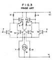
- Fig. 3 shows a circuit diagram of a typical conventional Flip-Flop circuit having a set signal input and a reset signal input.
- the Flip-Flop circuit shown in Fig. 3 is an RS (for reset-set) Flip-Flop circuit and has the following construction.
- the RS Flip-Flop circuit comprises a first data holding transistor Q11 in which its collector is coupled to a higher potential power supply terminal V H through a resistor 5 and its emitter is connected to a lower potential power supply terminal V L through a common junction 17 and a constant-current source 18; a second data holding transistor Q12 wherein, likewise, its collector is coupled to the higher potential power supply terminal V H through a resistor 6 and its emitter is connected to the lower potential power supply terminal V L through the common junction 17 and the constant-current source 18; a set signal input transistor Q18 wherein its base is connected to a set signal input terminal S , its collector is connected to the collector of the first data holding transistor Q11 and its emitter is connected to the common junction 17; and a reset signal input transistor Q19 wherein its base is connected to a reset signal input terminal R , its collector is connected to the collector of the second data holding transistor Q12 and its emitter is connected to the common junction 17.
- the circuit further comprises a first feed-back emitter-follower transistor Q13 wherein its collector is directly connected to the higher potential power supply terminal V H , its base is connected to the tied together collectors of the first data holding transistor Q11 and the first input transistor Q18 and its emitter is connected to one output terminal 15 and to the base of the second data holding transistor Q12 through a resistor 9 and further to the lower potential power supply terminal V L through an emitter-follower load resistor 8; and a second feedback emitter-follower transistor Q14 wherein, likewise, its collector is directly connected to the higher potential power supply terminal V H , its base is connected to the tied together collectors of the second data holding transistor Q12 and the second input transistor Q19 and its emitter is connected to the other output terminal 16 and to the base of the first data holding transistor Q11 through a resistor 10 and further to the lower potential power supply terminal V L through an emitter-follower load resistor 7.
- a first feed-back emitter-follower transistor Q13 wherein its collector is directly connected to the higher potential
- the resistor 9 shown in Fig. 3 is the so-called level shifting resistor which, in order to avoid concurrence or interference between the high level of the base potential of the second data holding transistor Q12 and that of the set signal input transistor Q18, renders the high level of the base potential of the second data holding transistor Q12 to be lowered from the high level of the output terminal 15 by the voltage corresponding to the voltage drop developed across this level shifting resistor 9.
- the resistor 10 is also a level shifting resistor which renders the high level of the base potential of the first data holding transistor Q11 to be lower than that of the output terminal 16 by the voltage drop developed across this level shifting resistor 10, thereby avoiding the concurrence or interference between the high level of the base potential of the first data holding transistor Q11 and that of the reset signal input transistor Q19.
- the conventional Flip-Flop circuit as explained above has drawbacks in that it requires two level shifting resistors 9, 10 in addition to the indispensable resistors 5, 6 for establishing the necessary logical amplitude and the emitter-follower load resistors 7, 8, and in that a safety working range of the power supply voltages therefor is narrow because the level shift voltage developed across each of the level shifting resistors changes dependent upon the variation of the power supply voltage.
- an improved Flip-Flop circuit in which the provision of only one level shifting resistor is sufficient and the voltage drop developed across the level shifting resistor has no reliance upon the power supply voltage.
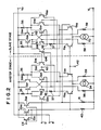
- Fig. 1 shows a circuit diagram of a Flip-Flop circuit as a first embodiment according to the present invention.
- the Flip-Flop circuit of this first embodiment comprises first and second data holding transistors Q11, Q12 wherein the respective emitters are tied together at a junction 22 and are connected to the lower potential power supply terminal V L through a level shifting resistor represented by a reference number 20 and a constant-current source 18, and the respective collectors are connected to the higher potential power supply terminal V H through the resistors 5, 6, respectively; a set signal input transistor Q18 wherein its base is connected to a set signal input terminal S , its collector is connected to the collector of the first data holding transistor Q11 and its emitter is connected to the common junction 21 between the resistor 20 and the constant-current source 18; a reset signal input transistor Q19 wherein its base is connected to a reset signal input terminal R , its collector is connected to the collector of the second data holding transistor Q12 and its emitter is connected to the common junction 21; a first feedback emitter-follower transistor Q13 wherein its collector is connected to the high potential power supply terminal V H , its base is
- both the set signal input terminal S and the reset signal input terminal R are of low levels and the one output terminal 15 is of a high level while the other output terminal 16 is of a low level as their initial state, the current is flowing in the passage defined by the resistor 6, the second data holding transistor Q12 and the level shifting resistor 20.
- the base potential of the second data holding transistor Q12 is of the same high level as of the high level of the set signal input terminal S .
- the voltage which is larger than the potential difference between the base and the emitter of the second data holding transistor Q12 by the potential difference developed across the resistor 20 is applied between the base and the emitter of the set signal input transistor Q18.
- the set signal input transistor Q18 changes from its non-conducting state to its conducting state and the second data holding transistor Q12 changes from its conducting state to its non-conducting state
- the one output terminal 15 goes to a low level and the other output terminal 16 goes to a high level. That is, the current passage is changed from one defined by the resistor 6, the second data holding transistor Q12 and the common level shifting resistor 20 to the other one defined by the resistor 5, the first data holding transistor Q11 and the common resistor 20.
- Fig. 2 shows a circuit diagram of a Flip-Flop circuit as a second embodiment according to the present invention.
- the Flip-Flop circuit shown in Fig. 2 is a typical master-slave D-type Flip-Flop circuit which has a master stage at the left-hand side from the dotted line and a slave stage at the right-hand side from the same dotted line.
- the master stage of the Flip-Flop circuit comprises a plurality of NPN bipolar transistors Q22 - Q33, a constant-current source 34, a plurality of resistors 35 - 41, a clock signal input terminal CK, a data signal input terminal D , a reset signal input terminal R , a first reference voltage input terminal 60 and a second reference voltage input terminal 42.
- the emitters of the two data holding transistors Q22, Q23 are directly connected with each other at a junction 81 and they, together with the emitter of the reset signal input transistor Q26, are further connected to the collector of the transistor Q32 constituting a first differential circuit of lower second logical level through the level shifting resistor 37. As shown in the drawings, only one level shifting resistor 37 is provided in the master stage circuit.
- the slave stage includes a plurality of NPN bipolar transistors Q46 - Q54, a plurality of resistors 55 - 59, a constant-current source 70, a higher potential power supply terminal V H , a lower potential power supply terminal V L , and a pair of output terminals 61 and 62.
- the emitters of the two data holding transistors Q46, Q47 are directly connected with each other at a junction 82 and they, together with the emitter of the reset signal input transistor Q50, are further connected to the collector of the transistor Q51 constituting a second differential circuit of lower second logical level through the level shifting resistor 57.
- only one level shifting resistor 57 is provided in the slave stage circuit as in the master stage circuit.
- the circuit at the master stage reads-in the data to be held next by the transistors Q24, Q25 and, the circuit at the slave stage holds the previous data at the output terminals 61, 62 by the data holding transistors Q46, Q47.
- the circuit at the master stage holds by the first and second data holding transistors Q22, Q23 the data read-in and, upon receiving such data from the master stage, the circuit at the slave stage outputs them to the output terminals 61, 62 by the data holding transistors Q46, Q47.
- the effective resetting is ensured because, due to the level shifting resistors 37 and 57 respectively provided in the master stage circuit and the slave stage circuit as in the first embodiment, the high level of the reset signal input terminal R does not interfere or concur with the high level at the bases of the data holding transistors Q22, Q23 in the master stage and of the data holding transistors Q46, Q47 in the slave stage.
- the present invention brings about advantages over the prior art in that only one resistor is sufficient as the level shifting resistor required for preventing interference or concurrence between the high level of the set signal or reset signal and the high level of the internal data held by the respective data holding transistors, which contributes to an increase in integration or packing density of the circuit, and in that the level shift voltage developed across this level shifting resistor does not rely on variation of the power supply voltage, which allows a larger working range of power supply voltages.
- the transistors used have been specified as being NPN-type bipolar transistors, it will be understood that PNP-type bipolar transistors may also be utilized with appropriate changes being made in the polarities of the power supply sources.
Landscapes
- Engineering & Computer Science (AREA)
- Power Engineering (AREA)
- Bipolar Integrated Circuits (AREA)
- Logic Circuits (AREA)
- Electronic Switches (AREA)
Applications Claiming Priority (2)
| Application Number | Priority Date | Filing Date | Title |
|---|---|---|---|
| JP150091/89 | 1989-06-12 | ||
| JP1150091A JPH0313116A (ja) | 1989-06-12 | 1989-06-12 | フリップフロップ回路 |
Publications (2)
| Publication Number | Publication Date |
|---|---|
| EP0403215A2 true EP0403215A2 (fr) | 1990-12-19 |
| EP0403215A3 EP0403215A3 (fr) | 1993-07-21 |
Family
ID=15489318
Family Applications (1)
| Application Number | Title | Priority Date | Filing Date |
|---|---|---|---|
| EP19900306371 Withdrawn EP0403215A3 (fr) | 1989-06-12 | 1990-06-12 | Circuit flip-flop |
Country Status (2)
| Country | Link |
|---|---|
| EP (1) | EP0403215A3 (fr) |
| JP (1) | JPH0313116A (fr) |
Cited By (1)
| Publication number | Priority date | Publication date | Assignee | Title |
|---|---|---|---|---|
| US5604456A (en) * | 1995-01-17 | 1997-02-18 | Kabushiki Kaisha Toshiba | Differential RS latch circuit |
Family Cites Families (11)
| Publication number | Priority date | Publication date | Assignee | Title |
|---|---|---|---|---|
| USRE27928E (en) * | 1965-06-01 | 1974-02-26 | Gated flip-flop employing plural transistors and plural capacitors cooperating to minimize flip-flop recovery time | |
| US3440449A (en) * | 1966-12-07 | 1969-04-22 | Motorola Inc | Gated dc coupled j-k flip-flop |
| CH497087A (de) * | 1968-11-07 | 1970-09-30 | Centre Electron Horloger | Binärer Frequenzteiler |
| DE2221331C3 (de) * | 1972-04-29 | 1981-01-22 | Licentia Patent-Verwaltungs-Gmbh, 6000 Frankfurt | Elektronischer Folgeschalter mit Halteschaltung |
| US3818250A (en) * | 1973-02-07 | 1974-06-18 | Motorola Inc | Bistable multivibrator circuit |
| JPS5931892B2 (ja) * | 1976-11-19 | 1984-08-04 | 日本電気株式会社 | 半導体集積回路 |
| JPS5561144A (en) * | 1978-10-31 | 1980-05-08 | Nec Corp | Logic circuit |
| PT74627B (en) * | 1981-04-01 | 1983-08-22 | Rca Corp | Flip-flop circuit |
| JPS5925421A (ja) * | 1982-08-03 | 1984-02-09 | Toshiba Corp | 同期式論理回路 |
| JPS62222712A (ja) * | 1986-03-25 | 1987-09-30 | Toshiba Corp | フリツプフロツプ回路 |
| DE3875878T2 (de) * | 1987-08-29 | 1993-06-09 | Nippon Electric Co | Mit hoher schnelligkeit betreibbares und zur implementierung als integrierter schaltkreis geeigneter flipflop. |
-
1989
- 1989-06-12 JP JP1150091A patent/JPH0313116A/ja active Pending
-
1990
- 1990-06-12 EP EP19900306371 patent/EP0403215A3/fr not_active Withdrawn
Cited By (1)
| Publication number | Priority date | Publication date | Assignee | Title |
|---|---|---|---|---|
| US5604456A (en) * | 1995-01-17 | 1997-02-18 | Kabushiki Kaisha Toshiba | Differential RS latch circuit |
Also Published As
| Publication number | Publication date |
|---|---|
| JPH0313116A (ja) | 1991-01-22 |
| EP0403215A3 (fr) | 1993-07-21 |
Similar Documents
| Publication | Publication Date | Title |
|---|---|---|
| US4560888A (en) | High-speed ECL synchronous logic circuit with an input logic circuit | |
| US4041326A (en) | High speed complementary output exclusive OR/NOR circuit | |
| EP0186260B1 (fr) | Circuit de porte logique à émetteurs couplés | |
| EP0375979A2 (fr) | Circuit d'attaque BICMOS pour circuits logiques CMOS à haute densité | |
| US3473047A (en) | High speed digital logic circuit having non-saturating output transistor | |
| US3617776A (en) | Master slave flip-flop | |
| US4517475A (en) | Master-slave flip-flop arrangement with slave section having a faster output transistion and a greater resistance to output degradation | |
| US3424928A (en) | Clocked r-s flip-flop | |
| US4355246A (en) | Transistor-transistor logic circuit | |
| EP0403215A2 (fr) | Circuit flip-flop | |
| US4801825A (en) | Three level state logic circuit having improved high voltage to high output impedance transition | |
| US5661426A (en) | Logic circuit | |
| US4491745A (en) | TTL flip-flop with clamping diode for eliminating race conditions | |
| JP2760017B2 (ja) | 論理回路 | |
| US4970416A (en) | Emitter coupled logic circuit having rapid output voltage | |
| US4270062A (en) | "D" Flip-flop | |
| US4578599A (en) | Flip-flop having improved synchronous reset | |
| US3917959A (en) | High speed counter latch circuit | |
| EP0076099A2 (fr) | Circuit TTL | |
| EP0155305B1 (fr) | Logique couplee sur le collecteur et l'emetteur | |
| RU2827115C1 (ru) | Триггерный синхронный d триггер | |
| US4007384A (en) | Noninverting current-mode logic gate | |
| JPS6316047B2 (fr) | ||
| JPH071865B2 (ja) | エミッタ結合論理回路 | |
| JP2681938B2 (ja) | フリツプフロツプ |
Legal Events
| Date | Code | Title | Description |
|---|---|---|---|
| PUAI | Public reference made under article 153(3) epc to a published international application that has entered the european phase |
Free format text: ORIGINAL CODE: 0009012 |
|
| 17P | Request for examination filed |
Effective date: 19900620 |
|
| AK | Designated contracting states |
Kind code of ref document: A2 Designated state(s): DE FR GB |
|
| PUAL | Search report despatched |
Free format text: ORIGINAL CODE: 0009013 |
|
| RHK1 | Main classification (correction) |
Ipc: H03K 3/286 |
|
| AK | Designated contracting states |
Kind code of ref document: A3 Designated state(s): DE FR GB |
|
| 17Q | First examination report despatched |
Effective date: 19951010 |
|
| STAA | Information on the status of an ep patent application or granted ep patent |
Free format text: STATUS: THE APPLICATION IS DEEMED TO BE WITHDRAWN |
|
| 18D | Application deemed to be withdrawn |
Effective date: 19960423 |