EP0404246A1 - Dispositif semiconducteur pour engendrer un courant d'électrons - Google Patents
Dispositif semiconducteur pour engendrer un courant d'électrons Download PDFInfo
- Publication number
- EP0404246A1 EP0404246A1 EP90201575A EP90201575A EP0404246A1 EP 0404246 A1 EP0404246 A1 EP 0404246A1 EP 90201575 A EP90201575 A EP 90201575A EP 90201575 A EP90201575 A EP 90201575A EP 0404246 A1 EP0404246 A1 EP 0404246A1
- Authority
- EP
- European Patent Office
- Prior art keywords
- semiconductor device
- type
- semiconductor
- region
- thickness
- Prior art date
- Legal status (The legal status is an assumption and is not a legal conclusion. Google has not performed a legal analysis and makes no representation as to the accuracy of the status listed.)
- Granted
Links
- 239000004065 semiconductor Substances 0.000 title claims abstract description 68
- 230000015556 catabolic process Effects 0.000 claims abstract description 5
- 230000001133 acceleration Effects 0.000 claims description 12
- 238000010894 electron beam technology Methods 0.000 claims description 8
- 229910052710 silicon Inorganic materials 0.000 claims description 8
- 239000010703 silicon Substances 0.000 claims description 8
- 229910052792 caesium Inorganic materials 0.000 claims description 7
- TVFDJXOCXUVLDH-UHFFFAOYSA-N caesium atom Chemical compound [Cs] TVFDJXOCXUVLDH-UHFFFAOYSA-N 0.000 claims description 7
- 239000000463 material Substances 0.000 claims description 7
- 229910052788 barium Inorganic materials 0.000 claims description 2
- DSAJWYNOEDNPEQ-UHFFFAOYSA-N barium atom Chemical compound [Ba] DSAJWYNOEDNPEQ-UHFFFAOYSA-N 0.000 claims description 2
- 229910021420 polycrystalline silicon Inorganic materials 0.000 claims description 2
- 239000012535 impurity Substances 0.000 claims 1
- 230000000694 effects Effects 0.000 abstract description 9
- 230000007423 decrease Effects 0.000 abstract description 6
- 239000010410 layer Substances 0.000 description 25
- XUIMIQQOPSSXEZ-UHFFFAOYSA-N Silicon Chemical compound [Si] XUIMIQQOPSSXEZ-UHFFFAOYSA-N 0.000 description 7
- 238000010586 diagram Methods 0.000 description 5
- 238000000034 method Methods 0.000 description 4
- 238000001493 electron microscopy Methods 0.000 description 3
- 238000010438 heat treatment Methods 0.000 description 3
- 238000005381 potential energy Methods 0.000 description 3
- 238000004519 manufacturing process Methods 0.000 description 2
- 239000002344 surface layer Substances 0.000 description 2
- JBRZTFJDHDCESZ-UHFFFAOYSA-N AsGa Chemical compound [As]#[Ga] JBRZTFJDHDCESZ-UHFFFAOYSA-N 0.000 description 1
- QVGXLLKOCUKJST-UHFFFAOYSA-N atomic oxygen Chemical compound [O] QVGXLLKOCUKJST-UHFFFAOYSA-N 0.000 description 1
- 239000010406 cathode material Substances 0.000 description 1
- 150000001875 compounds Chemical class 0.000 description 1
- 230000003247 decreasing effect Effects 0.000 description 1
- 230000001627 detrimental effect Effects 0.000 description 1
- 239000002019 doping agent Substances 0.000 description 1
- 238000005265 energy consumption Methods 0.000 description 1
- 230000008020 evaporation Effects 0.000 description 1
- 238000001704 evaporation Methods 0.000 description 1
- 230000002349 favourable effect Effects 0.000 description 1
- 239000007789 gas Substances 0.000 description 1
- 238000001459 lithography Methods 0.000 description 1
- 238000001451 molecular beam epitaxy Methods 0.000 description 1
- 230000003287 optical effect Effects 0.000 description 1
- 239000001301 oxygen Substances 0.000 description 1
- 229910052760 oxygen Inorganic materials 0.000 description 1
- 239000002244 precipitate Substances 0.000 description 1
- 238000001228 spectrum Methods 0.000 description 1
- 239000000758 substrate Substances 0.000 description 1
- XLYOFNOQVPJJNP-UHFFFAOYSA-N water Substances O XLYOFNOQVPJJNP-UHFFFAOYSA-N 0.000 description 1
Images
Classifications
-
- H—ELECTRICITY
- H01—ELECTRIC ELEMENTS
- H01J—ELECTRIC DISCHARGE TUBES OR DISCHARGE LAMPS
- H01J1/00—Details of electrodes, of magnetic control means, of screens, or of the mounting or spacing thereof, common to two or more basic types of discharge tubes or lamps
- H01J1/02—Main electrodes
- H01J1/30—Cold cathodes, e.g. field-emissive cathode
- H01J1/308—Semiconductor cathodes, e.g. cathodes with PN junction layers
Definitions
- the invention relates to a semiconductor device for generating an electron current, comprising a cathode having a semiconductor body with at least an n-type semiconductor region and a first p- type semiconductor region, in which electrons leaving the semiconductor body at a surface can be generated in said body by giving the n-type region a positive bias with respect to the p-type region.
- the invention also relates to a pick-up tube and a display device provided with such a semiconductor device.
- thermionic cathodes are used, inter alia, in cathode ray tubes in which they replace the conventional thermionic cathode in which electron emission is generated by heating. In addition they are used in, for example, apparatus for electron microscopy.
- thermionic cathodes have the drawback that they are not immediately ready for operation because they have to be heated sufficiently before emission occurs. Moreover, the cathode material is eventually lost due to evaporation, so that these cathodes have a limited lifetime.
- the cold cathodes known from the above-mentioned Patent Application are based on the emission of electrons from the semiconductor body when a pn junction is operated in the reverse direction in such a manner that avalanche multiplication occurs. Some electrons may then obtain as much kinetic energy as is required to exceed the electron work function; these electrons are then liberated on the surface and thus supply an electron current.
- the cathodes described in said Patent Application are provided with an acceleration or gate electrode.
- the aim is to have a maximum possible efficiency, which can be achieved, inter alia, by a minimum possible work function for the electrons.
- the latter is realised, for example, by providing the surface of the cathode with a layer of material which decreases the work function.
- Cesium is preferably used for this purpose because it produces a maximum decrease of the electron work function.
- cesium may have drawbacks.
- cesium is very sensitive to the presence (in its ambience) of oxidising gases (water vapour, oxygen, C0 2 ).
- cesium is fairly volatile, which may be detrimental in those uses in which substrates or compounds are present in the vicinity of the cathode such as may be the case, for example, in electron lithography or electron microscopy. The evaporated cesium may then precipitate on these objects.
- Netherlands Patent Application no. 8600675 (PHN 11.670) in the name of the Applicant proposes to provide an intrinsic semiconductor layer between the p-type region and the n-type region.
- the substantially intrinsic layer introduces in the semiconductor device a region which in the operating condition is completely depleted and in which a maximum field strength prevails substantially throughout this region.
- the electrons are generated earlier and at a higher potential energy, while the generated electrons in the intrinsic part undergo a slight scattering of ionised dopant atoms so that the effective free path length is increased.
- a semiconductor device is characterized in that the n-type region has a thickness of at most 4 nanometers. This thickness is preferably smaller than 2 nanometers.
- the invention is based, inter alia, on the recognition that quantisation effects occur at such a small thickness (one or several atomic layers) so that the effective work function is decreased.
- n-type (or p-type) layer may comprise a partly intrinsic top layer due to the special way of providing the structures.
- This Application refers to thin n-type or p-type layers, such a double layer of an n-type or p-type layer and a thin intrinsic layer is also included.
- An intrinsic layer is then understood to mean a ⁇ -type or 7 r-type layer with a doping of at most 5.10 16 atoms/cm 3 .
- the thin n-type layer may also be deliberately separated from the p-type region by an intrinsic semiconductor layer, similarly as described in Netherlands Patent Application no. 8600675 (PHN 11.670) in the name of the Applicant.
- a preferred embodiment of the invention is therefore characterized in that the n-type region is present between the first ptype region and a second p-type surface region.
- This second p-type surface region has preferably also a thickness of at most 4 nanometers.
- An additional advantage of such a device is that, notably for silicon, the distance between the bottom of the conduction band and the vacuum level at some distance from the surface is lower for p-type silicon than for n-type silicon.
- the second p-type surface region preferably has a thickness of at most 2 micrometers, for example, by forming it again as a "Planar Doping" structure. A part of the first p-type region may also be realised in such a manner.
- a semiconductor device is characterized in that the surface has an electrically insulating layer in which at least one aperture is provided, while at least one acceleration electrode is arranged on the insulating layer at the edge of the aperture, and the semiconductor structure, at least within the aperture, locally has a lower breakdown voltage than the other part of the semiconductor structure.
- a cathode according to the invention may be advantageously used in a pick-up tube, while there are also various uses for a display device comprising a semiconductor cathode according to the invention.
- a display device comprising a semiconductor cathode according to the invention.
- One use is, for example, a display tube having a fluorescent screen which is activated by the electron current originating from the semiconductor device.
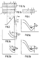
- the advantages of a semiconductor device according to the invention will now be described with reference to Figs. 1 to 3 and compared with those as described in Netherlands Patent Application no. 7905470.
- the device described in this Application (Fig. 1a) comprises at a main surface 2 of a semiconductor body 1 an n-type surface region 3 constituting a pn junction 8 with a p-type region 4.
- the regions 3 and 4 may be biased in the reverse direction with respect to each other so that avalanche multiplication occurs. A part of the electrons which are then liberated may then obtain as much energy as is required to be emitted from the semiconductor body.
- the n-type surface region 3 has a thickness of at most 4 nanometers (for example, 2 nanometers).
- the p-type region 4 is completely depleted during use.
- the p-type regions are possibly contacted via a p region 5.
- Fig. 2 shows diagrammatically the variation of the field strength for the two devices.
- a maximum field occurs at the area of the pn junction 8, which field decreases to the value of zero on both sides of the junction at the edges of the depletion zone (line a, b).
- Such a field variation leads to an electron energy diagram as is shown by means of drawn lines in Fig. 3a for the device of Fig. 1a.
- the electron work function is initially zero until it increases in the depletion zone to a value of approximately 0.8 volt (in silicon) at the area of the pn junction. Since it holds that ax dV and the field E decreases from this point (see Fig. 2, line a), the curve a in Fig. 3a increases less and less steeply from this point until the electron work function remains constant from the edge of the depletion zone.
- a similar curve for the device of Fig. 1b differs from that of Fig. 3a in that the electron work function will steeply increase at approximately 2 nanometers from the surface (see Fig. 3b) due to the small thickness of the n-type region 3.
- the electrons To be able to reach the vacuum, the electrons must have an energy which is at least equal to the emission energy ⁇ .
- d b in the device according to the invention is small with respect to the thickness d a in the device of Fig. 1, it holds that d b ⁇ d a , while ⁇ a ⁇ X b so that P b > P a .
- n-type region 3 is present between a p-type region 4 and a p-type surface region 7.
- the n-type region 3 is only several atomic layers thick so that quantisation effects occur of the energy levels and the (quasi) Fermi level comes above the bottom of the conduction band of the n-type region 3 (Fig. 5a).
- the electron work function in the region 3 increases until the quasi Fermi level coincides with the bottom of the conduction band of the (preferably highly doped) p- type surface region 7.
- Electrons which are generated by simultaneous occurrence of avalanche breakdown of the pn junction 8 fill up the energy levels and cross, as it were, the p-type surface region.
- a small layer thickness ( ⁇ 4 nanometers) and a high doping is preferably chosen for this p-type region.
- the p + -type surface layer 7 may alternatively be provided by means of techniques resulting in "6-doping or "Planar Doping" structures, i.e. techniques which in addition to other suitable techniques (molecular beam epitaxy) can also be used for manufacturing the n-type surface layer 3 in the device of Fig. 1 b. In this respect it may be advantageous to manufacture the p-type layer 4 and/or possible intermediate intrinsic layers by means of this technique.
- a semiconductor cathode according to the invention may have an insulating layer at its surface 2 on which acceleration electrodes are arranged around apertures for the purpose of emission; the possible forms of the emitting regions and the acceleration electrodes have been described in greater detail in the above-mentioned Netherlands Patent Application no. 7905470.
- the aperture may be slit-shaped or circular with a gap width or circle diameter of the same order of magnitude as the thickness of the insulating layer.
- the semiconductor structure usually has a lower breakdown voltage at the area of such apertures.
- the acceleration electrode (of, for example polycrystalline silicon) may be split up in different manners in which, for example, a part is located inside and another part is located outside a circular gap.
- the surface may be coated, if desired, with a work function-decreasing material such as cesium or barium.
- a work function-decreasing material such as cesium or barium.
- silicon it is alternatively possible to choose an A3-B5 semiconductor material (gallium ar
- Semiconductor cathodes according to the invention can be used in pick-up tubes as well as display tubes, but also, for example in electron microscopy.
Landscapes
- Cold Cathode And The Manufacture (AREA)
- Electrodes For Cathode-Ray Tubes (AREA)
Applications Claiming Priority (2)
| Application Number | Priority Date | Filing Date | Title |
|---|---|---|---|
| NL8901590A NL8901590A (nl) | 1989-06-23 | 1989-06-23 | Halfgeleiderinrichting voor het opwekken van een elektronenstroom. |
| NL8901590 | 1989-06-23 |
Publications (2)
| Publication Number | Publication Date |
|---|---|
| EP0404246A1 true EP0404246A1 (fr) | 1990-12-27 |
| EP0404246B1 EP0404246B1 (fr) | 1994-06-01 |
Family
ID=19854892
Family Applications (1)
| Application Number | Title | Priority Date | Filing Date |
|---|---|---|---|
| EP19900201575 Expired - Lifetime EP0404246B1 (fr) | 1989-06-23 | 1990-06-18 | Dispositif semiconducteur pour engendrer un courant d'électrons |
Country Status (4)
| Country | Link |
|---|---|
| EP (1) | EP0404246B1 (fr) |
| JP (1) | JPH0330230A (fr) |
| DE (1) | DE69009303T2 (fr) |
| NL (1) | NL8901590A (fr) |
Citations (2)
| Publication number | Priority date | Publication date | Assignee | Title |
|---|---|---|---|---|
| EP0241956A1 (fr) * | 1986-03-17 | 1987-10-21 | Koninklijke Philips Electronics N.V. | Dispositif semi-conducteur pour générer un courant électronique |
| EP0257460A2 (fr) * | 1986-08-12 | 1988-03-02 | Canon Kabushiki Kaisha | Générateur de faisceau d'électrons à l'état solide |
-
1989
- 1989-06-23 NL NL8901590A patent/NL8901590A/nl not_active Application Discontinuation
-
1990
- 1990-06-18 EP EP19900201575 patent/EP0404246B1/fr not_active Expired - Lifetime
- 1990-06-18 DE DE1990609303 patent/DE69009303T2/de not_active Expired - Fee Related
- 1990-06-20 JP JP2160029A patent/JPH0330230A/ja active Pending
Patent Citations (2)
| Publication number | Priority date | Publication date | Assignee | Title |
|---|---|---|---|---|
| EP0241956A1 (fr) * | 1986-03-17 | 1987-10-21 | Koninklijke Philips Electronics N.V. | Dispositif semi-conducteur pour générer un courant électronique |
| EP0257460A2 (fr) * | 1986-08-12 | 1988-03-02 | Canon Kabushiki Kaisha | Générateur de faisceau d'électrons à l'état solide |
Also Published As
| Publication number | Publication date |
|---|---|
| JPH0330230A (ja) | 1991-02-08 |
| DE69009303T2 (de) | 1994-12-08 |
| DE69009303D1 (de) | 1994-07-07 |
| EP0404246B1 (fr) | 1994-06-01 |
| NL8901590A (nl) | 1991-01-16 |
Similar Documents
| Publication | Publication Date | Title |
|---|---|---|
| US4801994A (en) | Semiconductor electron-current generating device having improved cathode efficiency | |
| US4766340A (en) | Semiconductor device having a cold cathode | |
| US4683399A (en) | Silicon vacuum electron devices | |
| US4554564A (en) | Semiconductor device and method of manufacturing same, as well as a pick-up device and a display device having such a semiconductor device | |
| US3581151A (en) | Cold cathode structure comprising semiconductor whisker elements | |
| GB2109156A (en) | Cathode-ray device and semiconductor cathodes | |
| EP0395158B1 (fr) | Dispositif générateur d'électrons et dispositif d'affichage | |
| US5138402A (en) | Semiconductor electron emitting device | |
| US4506284A (en) | Electron sources and equipment having electron sources | |
| US3808477A (en) | Cold cathode structure | |
| US5243197A (en) | Semiconductor device for generating an electron current | |
| US4890031A (en) | Semiconductor cathode with increased stability | |
| US4853754A (en) | Semiconductor device having cold cathode | |
| EP0404246B1 (fr) | Dispositif semiconducteur pour engendrer un courant d'électrons | |
| GB2169132A (en) | Cathode-ray tube having an ion trap | |
| US6198210B1 (en) | Electron tube having a semiconductor cathode with lower and higher bandgap layers | |
| JP2735118B2 (ja) | 冷陰極真空管 | |
| JPH06162918A (ja) | 半導体電子放出素子並びにその製造方法 | |
| JP3403165B2 (ja) | 電子放出素子の製造方法 | |
| JP3102783B2 (ja) | 外部電界を利用して電子放出を活性化させた冷陰極電子放出素子 | |
| US3979629A (en) | Semiconductor with surface insulator having immobile charges | |
| Hoeberechts | Novel silicon avalanche diode as a direct modulated cathode with integrated planar electron-optics | |
| Deasley et al. | Electron emission from forward biased PN junctions |
Legal Events
| Date | Code | Title | Description |
|---|---|---|---|
| PUAI | Public reference made under article 153(3) epc to a published international application that has entered the european phase |
Free format text: ORIGINAL CODE: 0009012 |
|
| AK | Designated contracting states |
Kind code of ref document: A1 Designated state(s): DE FR GB IT NL |
|
| 17P | Request for examination filed |
Effective date: 19910620 |
|
| 17Q | First examination report despatched |
Effective date: 19930712 |
|
| GRAA | (expected) grant |
Free format text: ORIGINAL CODE: 0009210 |
|
| AK | Designated contracting states |
Kind code of ref document: B1 Designated state(s): DE FR GB IT NL |
|
| PG25 | Lapsed in a contracting state [announced via postgrant information from national office to epo] |
Ref country code: IT Free format text: LAPSE BECAUSE OF FAILURE TO SUBMIT A TRANSLATION OF THE DESCRIPTION OR TO PAY THE FEE WITHIN THE PRE;WARNING: LAPSES OF ITALIAN PATENTS WITH EFFECTIVE DATE BEFORE 2007 MAY HAVE OCCURRED AT ANY TIME BEFORE 2007. THE CORRECT EFFECTIVE DATE MAY BE DIFFERENT FROM THE ONE RECORDED.SCRIBED TIME-LIMIT Effective date: 19940601 Ref country code: NL Effective date: 19940601 |
|
| REF | Corresponds to: |
Ref document number: 69009303 Country of ref document: DE Date of ref document: 19940707 |
|
| ET | Fr: translation filed | ||
| NLV1 | Nl: lapsed or annulled due to failure to fulfill the requirements of art. 29p and 29m of the patents act | ||
| PLBE | No opposition filed within time limit |
Free format text: ORIGINAL CODE: 0009261 |
|
| STAA | Information on the status of an ep patent application or granted ep patent |
Free format text: STATUS: NO OPPOSITION FILED WITHIN TIME LIMIT |
|
| 26N | No opposition filed | ||
| REG | Reference to a national code |
Ref country code: FR Ref legal event code: CD |
|
| PGFP | Annual fee paid to national office [announced via postgrant information from national office to epo] |
Ref country code: GB Payment date: 19970602 Year of fee payment: 8 |
|
| PGFP | Annual fee paid to national office [announced via postgrant information from national office to epo] |
Ref country code: FR Payment date: 19970624 Year of fee payment: 8 |
|
| PGFP | Annual fee paid to national office [announced via postgrant information from national office to epo] |
Ref country code: DE Payment date: 19970822 Year of fee payment: 8 |
|
| PG25 | Lapsed in a contracting state [announced via postgrant information from national office to epo] |
Ref country code: GB Free format text: LAPSE BECAUSE OF NON-PAYMENT OF DUE FEES Effective date: 19980618 |
|
| GBPC | Gb: european patent ceased through non-payment of renewal fee |
Effective date: 19980618 |
|
| PG25 | Lapsed in a contracting state [announced via postgrant information from national office to epo] |
Ref country code: FR Free format text: LAPSE BECAUSE OF NON-PAYMENT OF DUE FEES Effective date: 19990226 |
|
| PG25 | Lapsed in a contracting state [announced via postgrant information from national office to epo] |
Ref country code: DE Free format text: LAPSE BECAUSE OF NON-PAYMENT OF DUE FEES Effective date: 19990401 |
|
| REG | Reference to a national code |
Ref country code: FR Ref legal event code: ST |