EP0405411A2 - Halbleiterspeicher mit einem verbesserten Datenleseschema - Google Patents
Halbleiterspeicher mit einem verbesserten Datenleseschema Download PDFInfo
- Publication number
- EP0405411A2 EP0405411A2 EP90112058A EP90112058A EP0405411A2 EP 0405411 A2 EP0405411 A2 EP 0405411A2 EP 90112058 A EP90112058 A EP 90112058A EP 90112058 A EP90112058 A EP 90112058A EP 0405411 A2 EP0405411 A2 EP 0405411A2
- Authority
- EP
- European Patent Office
- Prior art keywords
- output
- sense amplifier
- signal
- data
- circuit
- Prior art date
- Legal status (The legal status is an assumption and is not a legal conclusion. Google has not performed a legal analysis and makes no representation as to the accuracy of the status listed.)
- Granted
Links
- 239000004065 semiconductor Substances 0.000 title claims abstract description 17
- 230000004044 response Effects 0.000 claims abstract description 10
- 230000008859 change Effects 0.000 description 16
- 230000003213 activating effect Effects 0.000 description 12
- 238000010586 diagram Methods 0.000 description 12
- 239000011159 matrix material Substances 0.000 description 11
- 238000010276 construction Methods 0.000 description 7
- 230000000295 complement effect Effects 0.000 description 3
- 238000001514 detection method Methods 0.000 description 3
- 230000009849 deactivation Effects 0.000 description 2
- 230000004913 activation Effects 0.000 description 1
- 230000002411 adverse Effects 0.000 description 1
- 230000001934 delay Effects 0.000 description 1
- 230000009977 dual effect Effects 0.000 description 1
- 230000000694 effects Effects 0.000 description 1
- 230000006872 improvement Effects 0.000 description 1
- 230000001939 inductive effect Effects 0.000 description 1
- 230000003068 static effect Effects 0.000 description 1
Images






Classifications
-
- G—PHYSICS
- G11—INFORMATION STORAGE
- G11C—STATIC STORES
- G11C7/00—Arrangements for writing information into, or reading information out from, a digital store
- G11C7/10—Input/output [I/O] data interface arrangements, e.g. I/O data control circuits, I/O data buffers
- G11C7/1051—Data output circuits, e.g. read-out amplifiers, data output buffers, data output registers, data output level conversion circuits
- G11C7/106—Data output latches
-
- G—PHYSICS
- G11—INFORMATION STORAGE
- G11C—STATIC STORES
- G11C7/00—Arrangements for writing information into, or reading information out from, a digital store
- G11C7/10—Input/output [I/O] data interface arrangements, e.g. I/O data control circuits, I/O data buffers
- G11C7/1051—Data output circuits, e.g. read-out amplifiers, data output buffers, data output registers, data output level conversion circuits
Definitions
- This invention relates to a semiconductor memory, and more particularly to a readout circuit of a static memory.
- a known data readout circuit for a statis memory disclosed in U.S. Patent No. 4,766,572 is constructed on the basis of knowledge that a signal readout from a memory cell and amplified by a sense amplifier is transferred through a data latch circuit to an output circuit, and the delay associated with the activation of the data latch circuit is principal cause for the delay of data output, in such way that both the signal amplified by the sense amplifier and the output signal of the data latch circuit are applied to a switching circuit, and then the output of the switching circuit is supplied to the output circuit.
- the switching circuit allows transfer and output of the amplified signal. Once the sense amplifier is deactivated, it transfers the output of the data latch circuit to output it to the output circuit.
- the output signal is held at the data output terminal of the memory.
- the amplified signal from the sense amplifier is supplied to the output circuit before the data latch circuit is operated, and earlier according to such, output signal appears at the output terminal, with effect of reducing period of time between application of an address onto the memory and appearance of data output, that is access time.
- the switching circuit disconnects the output terminal thereof from the output terminal of the sense amplifier because of preventing the change in the potential at the output terminal of the sense amplifier resulting from the deactivation of the sense amplifier from affecting adversely the output of the switching circuit, that is, the output of the data latch circuit supplied to the output circuit.
- It is an object is to provide a semiconductor memory capable of readouting data at higher speed.
- Another object of the invention is to provide a semiconductor memory having an improved construction of readout circuit.
- the present invention is based on the knowledge of the readout circuit disclosed in U.S. Patent No. 4,766,572, that when the amplified signal is transferred from the sense amplifier through the switching circuit to the output circuit, considerable delay results because of the switching circuit.
- the switching circuit causes prolongation of the data (output) readout time by the sum of the time it takes for the switching gate permitting the transfer of the amplified signal to turn ON and the time it takes for the amplified signal to pass through the transfer gate.
- means for disconnecting the terminal of the sense amplifier from power supply when it is deactivated is provided to be connected to the sense amplifier so as to prevent the deactivation of it from inducing variation in the potential of the output terminal of it.
- the disconnection means makes it unnecessary to provide a switching gate between the output terminal of sense amplifier and the input terminal of the output circuit. According to the present invention, therefore, the output terminal of the sense amplifier is connected directly to the input terminal of the output circuit without the intermediation of switching gate.
- the output terminal of the sense amplifier is connected, for one thing, to the input terminal of the data latch circuit, and the output of the data latch circuit is connected to the input terminal of the output circuit through the switching gate of the switching circuit.
- the semiconductor memory comprises a sense amplifier for amplifying a data signal readout from selected memory cells, a latch circuit for latching the output signal of the sense amplifier, a switching circuit connected to the output terminal of the latch circuit, and an output circuit having an input terminal connected to the output terminal of the switching circuit and the output terminal of the sense amplifier and adapted for receiving at least one of the output signal from the sense amplifier and the output signal of the switching circuit and outputting a data output signal, the sense amplifier including means for making high impedance between the output of the sense amplifier and two terminals of power supply.
- the sense amplifier amplifies data signal in response to a first control signal and transfers the amplified data signal to the output terminal thereof
- the latch circuit latches the amplified output signal in response to a second control signal generated while the first control signal is generating
- the switching circuit turns ON and supplies the output signal of the latch circuit to the output circuit, in response to a third control signal during a desired period except the period of generating the first control signal, wherein high impedance is held between the output terminal of the sense amplifier and two terminals of power supply during a desired period of time except the period for generating the first control signal.
- the output signal of the sense amplifier can be applied to the output circuit without any delay, and this not only contributes to reducing the time it takes for readout data to appear at the output terminal of the output circuit or the data output terminal but also thereby enables faster data readout.
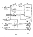
- an address buffer 101 detects change of address signal A i and outputs address change detection signal ⁇ i for a certain period as of 10 ns to a clock generator 113 and at the same time outputs complementary address buffer signals A i ′ and A i ′ to a X decoder 105 and Y decoder 106.
- a chip select buffer 102 upon receiving chip select signal CS , outputs chip select change signal ⁇ CS for a certain period to the clock generator 113 and simultaneously outputs chip select buffer signal CS′ to a data input control circuit 108 and a data output control circuit 112.
- signal WE′ from a write enable buffer and the signal CS′ activate the data control circuit 112 which outputs the input signal receiving at the input end of it from the output terminal D OUT of it.
- write enable buffer 104 outputs WE′ without outputting WE′.
- the data output control circuit 112 does not operated. Instead the data input control circuit 108 is operated and applied to data input terminal D IN .
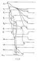
- Clock generator 113 receives two change detection signal ⁇ i and ⁇ CS and generates in turn four control signals ⁇ X , ⁇ S , ⁇ SW and ⁇ L as shown in Fig. 4.
- the clock generator firstly generates a word line activating signal ⁇ X which is supplied to a word line drive circuit 107. After the lapse of a certain period, it generates sense enable signal ⁇ S , which activates a sense amplifier in the memory cell matrix 109. After the lapse of another certain period, it also cause a switching signal ⁇ SW to rise and supplies the resulting signal to the switching circuit 114. After the lapse of a further certain period, it finally outputs a data latch signal ⁇ L to the data latch circuit 110 which is operated.
- the four control signals ⁇ L , ⁇ S , ⁇ SW , and ⁇ X drop in turn.
- Word line drive circuit 107 supplies X address signal X i from X address decoder 105 to word line W i as long as word line activating signal ⁇ X stays at high level.
- each bit line pair B L0 , B L0 , ..., B Li , B Li , ... get precharged to high level through a p-channel precharge transistor Q91 from power supply Vcc.
- Y address signal Y i from Y address decoder 106 causes one of CMOS transfer gates 902, 902 to turn ON and one of the bit line pair (in this prior art, BL i and BL i ) is connected to a pair of data lines DB and DB′ of the sense amplifier 903.
- both input transistors Q80 and Q81 sense amplifier 903 turn ON. Since the activating signal ⁇ S is at low level, however, n-channel transistor Q82 is in OFF state, and so no current flows. Electric charge is supplied from power supply Vcc through p-channel transistors Q83 and Q84 connected to form a current mirror circuit output, and thus the output terminal of input transistor Q80 is at high level. This is received by n-channel transistor Q86 of an inverter, which is in ON state. Accordingly the output terminal of the inverter, that is the output terminal RB of sense amplifier 903 is at low level.
- the rise of word line activating signal ⁇ X causes X address signal X i to be supplied to word line W i , and in turn, memory cell 901 is selected.
- a pair of bit lines BL i and BL i change in potential.
- change of ⁇ x causes change of bit line BL .
- the data line DB of sense amplifier 903 stays high level, DB goes to low level, input transistor Q80 turns ON, and input transistor Q81 turns OFF.
- sense amplifier activating signal ⁇ S rises, causing activating transistor Q82 to turn ON, resulting, in turn, in change of the output terminal of input transistor Q80 to low level, in turn-off of n- channel transistor Q86 and turn-on of p-channel transistor Q85 of the inverter, and in application of the high level of the power supply Vcc to output terminal RB.
- the output data of the selected cell within memory cell matrix 109 is amplified by sense amplifier 903 and output as an amplified signal RB.
- Output signal RB of the sense amplifier is supplied to both data latch circuit 110 and switching circuit 114.
- data latch circuit 110 is activated and the output LB of it rises.
- both the output RB of the snese amplifier and the output LB of the data latch circuit are input into the switching circuit 114.
- switching circuit 114 each input is connected to a common output SB through the first CMOS transfer gate consisting of n-channel transistor Q20 and p-channel transistor Q21 and the second CMOS transfer gate consisting of n-channel transistor Q23 and p-channel transistor Q24, respectively. While switcing control signal ⁇ SW is held at low level (before it rises), the second CMOS transfer gate is in ON state, and thus signal LB from the data latch circuit is supplied as switcing output SB to data output circuit 112.
- switching control signal ⁇ SW causes the second CMOS transfer gate to turn OFF, and instead the first CMOS transfer gate to turn ON, and thus signal RB from the sense amplifier is supplied as switching output SB to data output circuit 112.
- switching output SB rises and in turn, also output data D OUT rises and is output as a high level data.
- data latch circuit 110 still holds its output LB at high level.
- trailing switching control signal ⁇ SW causes the first and second CMOS transfer gates of switching circuit 114 to turn OFF and ON, respectively, and thus the switching output SB (which corresponds to inputs into data output circuit 110) is switched from sense amplifier output RB into latch circuit output LB.
- the data contents (high level) of it however remains unchanged.
- sense amplifier activating signal ⁇ S drops, and causes transistor Q82 in sense amplifier 903 (Fig. 3) to turn OFF, resulting in return of the output of transistor Q80 back to high level, which causing sense amplifier output RB to go to low level.
- readout of data output D OUT begins under the timing determined by the time when input of data output circuit (switching output SB in this prior art) begins to change.
- Readout output from the memory cell matrix that is, sense amplifier output RB
- this prior art has an disadvantage tht input into the data output circuit delays by period D0 with respect to the data readout from the sense amplifier.
- This delay D0 is expressed as D1 + D4, where D1 is the delay until the rise of switching signal ⁇ SW and D4 is the time it takes for the first CMOS transistor gate of switching circuit 114 to turns ON and then for sense amplifier output RB to transfer therethrough.
- delay time induced by the pass of the signal through the first CMOS transfer gate amounts to about 3 nS. It is noted that upon comparison with the access time of the semiconductor memory, assuming such as 30 nS, delay D0 is considerable.
- the first embodiment is different from the prior art illustrated in Figs. 1 through 3 in the following respects:
- Correspondent parts or components are designated by the same reference characters and description of them is omitted.
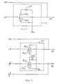
- the sense amplifier 503 of the first embodiment diagrammed schematically in Fig. 6 comprises input n-channel transistors Q50 and Q51 of which gates are connected to a pair of data lines DB and DB , respectively; input p-channel transistors Q53 and Q54 connected to the outputs of transistors Q50 and Q51, respectively, and constituting a current mirror circuit; and an activating n-channel transistor Q52 of which the gate receives sense amplifier activating signal ⁇ S and the other electrodes each are connected to the common terminal of input transistors Q50 and Q51 and ground, respectively; and a breaking p-channel transistor Q55 of which the gate receives sense amplifier activating signal ⁇ S through an inverter 400 and the other electrodes each are connected to the common source of p-channel transistors Q53 and Q54 and power supply Vcc, respectively.
- amplifier output RB outputs from the output terminal of input transistor Q51.
- enable signal ⁇ S When enable signal ⁇ S is held at high level, transistors Q52 and Q55 are in ON state, and hence the sense amplifier is held in activated state, during which readout data from the memory cells on data bus lines DB and DB is amplified and the amplified data is output at sense amplifier output RB.
- sense enable signal ⁇ S When sense enable signal ⁇ S is held at low level, both n-channel transistor Q52 and p-channel transistor Q55 are in OFF state so that high impedance stands between sense amplifier output RB, and power supply Vcc and ground GND, respectively. The potential of sense amplifier output RB therefore remains unchanged even if ⁇ S changes to low level, and in turn, data output circuit 112 is unaffected.
- sense amplifier output RB can be connected directly to data output circuit 112 without needing it to connect them through the transfer gate.
- Switching circuit 514 therefore, as shown in Fig. 7, comprises only transistors Q23, Q24 constituting the second CMOS transfer gate, and inverter 250, that is, those remaining as the result of the removal of Q23, Q24 constituting the second CMOS transfer gate from the prior art switching circuit shown in Fig. 2.
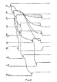
- address decoder output signal X i and address decoder output Y j change with changing address signal A i .
- address change detection signal ⁇ i is generated, resulting, in sequential rise (from low level to high level) of word line clock signal ⁇ X , switching control signal ⁇ SW , sense enable signal ⁇ S and data latch signal ⁇ L .
- rise of word line activating signal ⁇ X causes word line W i supplied with address decoder output signal X i , and nothing else, to rise from low level to high level, thereby data held in memory cell 901 begins to appear on bit lines BL, BL .
- switching control signal ⁇ SW rises, this causing transfer gate transistors Q23, Q24 between output LB of data latch 110 and latch output SB, that is, input of data output circuit 112 to turn OFF. Accordingly readout data appears, through sense amplifier 503, on readout data RB from sense amplifier and supplied directly to data output control circuit 112 without being disturbed by latch data LB. Then data D OUT of the same phase as that of readout data RB is output on the data output terminal.
- data latch signal ⁇ L rises after the lapse of a sufficient time following the appearance of readout data on readout data RB.
- sense amplifier 503 becomes again high impedance state.
- drop of switching control signal ⁇ SW causes transfer gate transistors Q23, Q24 of switching circuit 514 to turn ON so that data latch output LB is connected to input of data output circuit 112. Transfer gate transistors Q23, Q24 are in ON state, and hence latch output LB is connected to sense amplifier output RB, too.
- output terminal RB is in disconnected state to ground GND and power supply Vcc, and hence unchanged in potential, and in turn, latch data LB is unaffected.
- sense amplifier output RB can be applied directly to the data output circuit, this permitting delay D0 of access time due to intermediate of the transfer gate of the switching circuit in the prior art to nullify.
- high speed semiconductor memory device permitting in short access time can be realized by the construction that while sense amplifier is stayin gin nonoperative state, simultaneously sense amplifier is held in high impedance, state, as described above, so as to eliminate the transfer gate on the line which is a time delaying element or factor involved in access time.
- the second embodiment comprises sense amplifier 1202 (Fig. 9) of memory cell matrix 1201, data latch 1301 (Fig. 10) and switching circuit 1401 (Fig. 11) each in place of sense amplifier 503 of memory cell matrix 509, data latch 110 and switching circuit 514, respectively, in Example 1.
- Sense amplifier 1202 as diagrammed schematically in Fig. 9, is a parallel arrangement of two sense amplifiers 503 stated in the first embodiment such that two types of data lines DB, DB are connected in inverted relation to allow readout data from the sense amplifier to form complementary signals, that is, positive phase RB and inverse phase RB .
- This construction permits realization of fast access time compared with Example 1.
- each of data latch 1301 and switching circuit 1401 as diagrammed schematically in Fig.
- Sense amplifier readout data RB, RB is applied in parallel to latch circuit 1301 and connected to switching outputs SB, SB .
- Latch outputs LB, LB are input in parallel into switching circuit 1401.
- the second embodiment permits realization of semiconductor memory device having high speed access time by the construction of creating the state such that transfer gates on the lines which are involved in access time are removed.
Landscapes
- Static Random-Access Memory (AREA)
- Dram (AREA)
Applications Claiming Priority (2)
| Application Number | Priority Date | Filing Date | Title |
|---|---|---|---|
| JP16352189 | 1989-06-26 | ||
| JP163521/89 | 1989-06-26 |
Publications (3)
| Publication Number | Publication Date |
|---|---|
| EP0405411A2 true EP0405411A2 (de) | 1991-01-02 |
| EP0405411A3 EP0405411A3 (en) | 1992-08-26 |
| EP0405411B1 EP0405411B1 (de) | 1995-11-15 |
Family
ID=15775451
Family Applications (1)
| Application Number | Title | Priority Date | Filing Date |
|---|---|---|---|
| EP90112058A Expired - Lifetime EP0405411B1 (de) | 1989-06-26 | 1990-06-25 | Halbleiterspeicher mit einem verbesserten Datenleseschema |
Country Status (4)
| Country | Link |
|---|---|
| US (1) | US5051955A (de) |
| EP (1) | EP0405411B1 (de) |
| JP (1) | JPH0386997A (de) |
| DE (1) | DE69023556T2 (de) |
Families Citing this family (10)
| Publication number | Priority date | Publication date | Assignee | Title |
|---|---|---|---|---|
| US5146427A (en) * | 1989-08-30 | 1992-09-08 | Hitachi Ltd. | High speed semiconductor memory having a direct-bypass signal path |
| IL96808A (en) * | 1990-04-18 | 1996-03-31 | Rambus Inc | Introductory / Origin Circuit Agreed Using High-Performance Brokerage |
| JP2977296B2 (ja) * | 1991-02-19 | 1999-11-15 | 沖電気工業株式会社 | 半導体メモリ装置 |
| KR940010838B1 (ko) * | 1991-10-28 | 1994-11-17 | 삼성전자 주식회사 | 데이타 출력 콘트롤 회로 |
| KR950003014B1 (ko) * | 1992-07-31 | 1995-03-29 | 삼성전자 주식회사 | 반도체 메모리 장치의 번-인 테스트회로 및 번-인 테스트방법 |
| JP2819964B2 (ja) * | 1992-10-01 | 1998-11-05 | 日本電気株式会社 | 不揮発性半導体記憶装置 |
| JPH06162779A (ja) * | 1992-11-24 | 1994-06-10 | Oki Electric Ind Co Ltd | 半導体記憶装置におけるセンスアンプ制御回路 |
| JP3380050B2 (ja) * | 1994-07-14 | 2003-02-24 | 富士通株式会社 | 半導体記憶装置のデータ読み出し方法 |
| US5490114A (en) * | 1994-12-22 | 1996-02-06 | International Business Machines Corporation | High performance extended data out |
| US8437204B2 (en) * | 2009-06-12 | 2013-05-07 | Taiwan Semiconductor Manufacturing Company, Ltd. | Memory array with corresponding row and column control signals |
Family Cites Families (7)
| Publication number | Priority date | Publication date | Assignee | Title |
|---|---|---|---|---|
| JPS58169383A (ja) * | 1982-03-30 | 1983-10-05 | Fujitsu Ltd | 半導体記憶装置 |
| JPS60242582A (ja) * | 1984-05-16 | 1985-12-02 | Toshiba Corp | 半導体記憶装置のセンス増幅器 |
| JPS60254485A (ja) * | 1984-05-31 | 1985-12-16 | Nec Corp | スタテイツク型半導体記憶装置 |
| US4766572A (en) * | 1984-12-27 | 1988-08-23 | Nec Corporation | Semiconductor memory having a bypassable data output latch |
| DE3680064D1 (de) * | 1985-10-09 | 1991-08-08 | Nec Corp | Differenzverstaerker-schaltungsanordnung. |
| IT1200883B (it) * | 1985-12-13 | 1989-01-27 | Sgs Microelettronica Spa | Amplificatore sensore,particolarmente per memorie ram integrate in tecnologia mos |
| EP0303815B1 (de) * | 1987-08-18 | 1993-09-22 | Siemens Aktiengesellschaft | Leseverstärker für statische Speicher in CMOS-Technologie |
-
1990
- 1990-06-25 EP EP90112058A patent/EP0405411B1/de not_active Expired - Lifetime
- 1990-06-25 DE DE69023556T patent/DE69023556T2/de not_active Expired - Lifetime
- 1990-06-26 JP JP2167057A patent/JPH0386997A/ja active Pending
- 1990-06-26 US US07/543,526 patent/US5051955A/en not_active Expired - Lifetime
Also Published As
| Publication number | Publication date |
|---|---|
| DE69023556D1 (de) | 1995-12-21 |
| JPH0386997A (ja) | 1991-04-11 |
| EP0405411A3 (en) | 1992-08-26 |
| DE69023556T2 (de) | 1996-07-18 |
| US5051955A (en) | 1991-09-24 |
| EP0405411B1 (de) | 1995-11-15 |
Similar Documents
| Publication | Publication Date | Title |
|---|---|---|
| JPH05290581A (ja) | プレチャージ用出力ドライバ回路 | |
| US5777935A (en) | Memory device with fast write recovery and related write recovery method | |
| US5563835A (en) | Sense amplification in data memories | |
| KR970004821B1 (ko) | 출력회로 | |
| US5506522A (en) | Data input/output line sensing circuit of a semiconductor integrated circuit | |
| EP0405411B1 (de) | Halbleiterspeicher mit einem verbesserten Datenleseschema | |
| US5748556A (en) | Tristatable driver for internal data bus lines | |
| US5708607A (en) | Data read circuit of a memory | |
| US6292418B1 (en) | Semiconductor memory device | |
| US4858188A (en) | Semiconductor memory with improved write function | |
| US5295104A (en) | Integrated circuit with precharged internal data bus | |
| US5200710A (en) | Current mirror amplifier circuit and method of driving the same | |
| US5724299A (en) | Multiport register file memory using small voltage swing for write operation | |
| US5327317A (en) | Self-terminating data line driver | |
| US6633503B2 (en) | Voltage differential sensing circuit and methods of using same | |
| US5257226A (en) | Integrated circuit with self-biased differential data lines | |
| EP0547892B1 (de) | Integrierte Schaltung mit gegenseitig gesteuerten differenzialen Datenleitungen | |
| US5729160A (en) | Self-timed circuit control device and method | |
| JPH0883491A (ja) | データ読出回路 | |
| US4939392A (en) | Output circuit for driving a memory device output lead including a three-state inverting buffer and a transfer gate coupled between the buffer input lead and the buffer output lead | |
| US5646905A (en) | Self-clocking sense amplifier optimized for input signals close to VDD | |
| US4202045A (en) | Write circuit for a read/write memory | |
| US6115308A (en) | Sense amplifier and method of using the same with pipelined read, restore and write operations | |
| JPH03224200A (ja) | 半導体記憶装置 | |
| US4435791A (en) | CMOS Address buffer for a semiconductor memory |
Legal Events
| Date | Code | Title | Description |
|---|---|---|---|
| PUAI | Public reference made under article 153(3) epc to a published international application that has entered the european phase |
Free format text: ORIGINAL CODE: 0009012 |
|
| 17P | Request for examination filed |
Effective date: 19900725 |
|
| AK | Designated contracting states |
Kind code of ref document: A2 Designated state(s): DE FR GB |
|
| PUAL | Search report despatched |
Free format text: ORIGINAL CODE: 0009013 |
|
| AK | Designated contracting states |
Kind code of ref document: A3 Designated state(s): DE FR GB |
|
| 17Q | First examination report despatched |
Effective date: 19940503 |
|
| GRAA | (expected) grant |
Free format text: ORIGINAL CODE: 0009210 |
|
| AK | Designated contracting states |
Kind code of ref document: B1 Designated state(s): DE FR GB |
|
| REF | Corresponds to: |
Ref document number: 69023556 Country of ref document: DE Date of ref document: 19951221 |
|
| ET | Fr: translation filed | ||
| PLBE | No opposition filed within time limit |
Free format text: ORIGINAL CODE: 0009261 |
|
| STAA | Information on the status of an ep patent application or granted ep patent |
Free format text: STATUS: NO OPPOSITION FILED WITHIN TIME LIMIT |
|
| 26N | No opposition filed | ||
| REG | Reference to a national code |
Ref country code: GB Ref legal event code: IF02 |
|
| REG | Reference to a national code |
Ref country code: GB Ref legal event code: 732E |
|
| REG | Reference to a national code |
Ref country code: FR Ref legal event code: TQ |
|
| REG | Reference to a national code |
Ref country code: GB Ref legal event code: 732E |
|
| REG | Reference to a national code |
Ref country code: FR Ref legal event code: TP |
|
| PGFP | Annual fee paid to national office [announced via postgrant information from national office to epo] |
Ref country code: GB Payment date: 20090624 Year of fee payment: 20 Ref country code: DE Payment date: 20090619 Year of fee payment: 20 |
|
| REG | Reference to a national code |
Ref country code: GB Ref legal event code: PE20 Expiry date: 20100624 |
|
| PG25 | Lapsed in a contracting state [announced via postgrant information from national office to epo] |
Ref country code: GB Free format text: LAPSE BECAUSE OF EXPIRATION OF PROTECTION Effective date: 20100624 |
|
| PG25 | Lapsed in a contracting state [announced via postgrant information from national office to epo] |
Ref country code: DE Free format text: LAPSE BECAUSE OF EXPIRATION OF PROTECTION Effective date: 20100625 |
|
| PGFP | Annual fee paid to national office [announced via postgrant information from national office to epo] |
Ref country code: FR Payment date: 20090611 Year of fee payment: 20 |