EP0405576B1 - Dispositif de mémoire à semi-conducteur - Google Patents
Dispositif de mémoire à semi-conducteur Download PDFInfo
- Publication number
- EP0405576B1 EP0405576B1 EP90112452A EP90112452A EP0405576B1 EP 0405576 B1 EP0405576 B1 EP 0405576B1 EP 90112452 A EP90112452 A EP 90112452A EP 90112452 A EP90112452 A EP 90112452A EP 0405576 B1 EP0405576 B1 EP 0405576B1
- Authority
- EP
- European Patent Office
- Prior art keywords
- word lines
- semiconductor memory
- coupled
- voltage
- voltage source
- Prior art date
- Legal status (The legal status is an assumption and is not a legal conclusion. Google has not performed a legal analysis and makes no representation as to the accuracy of the status listed.)
- Expired - Lifetime
Links
- 239000004065 semiconductor Substances 0.000 title claims description 53
- 238000012360 testing method Methods 0.000 claims description 35
- 230000003068 static effect Effects 0.000 claims description 3
- 238000012216 screening Methods 0.000 description 18
- 238000012546 transfer Methods 0.000 description 16
- 239000003990 capacitor Substances 0.000 description 8
- 238000000034 method Methods 0.000 description 8
- 238000010586 diagram Methods 0.000 description 6
- 230000001133 acceleration Effects 0.000 description 4
- 230000005684 electric field Effects 0.000 description 4
- 238000009413 insulation Methods 0.000 description 3
- 239000012212 insulator Substances 0.000 description 3
- 230000002093 peripheral effect Effects 0.000 description 3
- 230000002950 deficient Effects 0.000 description 2
- 238000012986 modification Methods 0.000 description 2
- 230000004048 modification Effects 0.000 description 2
- 230000004888 barrier function Effects 0.000 description 1
- 230000015556 catabolic process Effects 0.000 description 1
- 230000000295 complement effect Effects 0.000 description 1
- 238000007796 conventional method Methods 0.000 description 1
- 230000007423 decrease Effects 0.000 description 1
- 230000007547 defect Effects 0.000 description 1
- 238000006731 degradation reaction Methods 0.000 description 1
- 230000000694 effects Effects 0.000 description 1
- 230000006870 function Effects 0.000 description 1
- 230000008569 process Effects 0.000 description 1
- 230000004044 response Effects 0.000 description 1
- 238000004904 shortening Methods 0.000 description 1
Images


Classifications
-
- G—PHYSICS
- G11—INFORMATION STORAGE
- G11C—STATIC STORES
- G11C29/00—Checking stores for correct operation ; Subsequent repair; Testing stores during standby or offline operation
-
- G—PHYSICS
- G11—INFORMATION STORAGE
- G11C—STATIC STORES
- G11C29/00—Checking stores for correct operation ; Subsequent repair; Testing stores during standby or offline operation
- G11C29/04—Detection or location of defective memory elements, e.g. cell constructio details, timing of test signals
- G11C29/50—Marginal testing, e.g. race, voltage or current testing
-
- G—PHYSICS
- G11—INFORMATION STORAGE
- G11C—STATIC STORES
- G11C29/00—Checking stores for correct operation ; Subsequent repair; Testing stores during standby or offline operation
- G11C29/04—Detection or location of defective memory elements, e.g. cell constructio details, timing of test signals
- G11C29/08—Functional testing, e.g. testing during refresh, power-on self testing [POST] or distributed testing
- G11C29/12—Built-in arrangements for testing, e.g. built-in self testing [BIST] or interconnection details
- G11C29/18—Address generation devices; Devices for accessing memories, e.g. details of addressing circuits
- G11C29/30—Accessing single arrays
- G11C29/34—Accessing multiple bits simultaneously
-
- G—PHYSICS
- G11—INFORMATION STORAGE
- G11C—STATIC STORES
- G11C11/00—Digital stores characterised by the use of particular electric or magnetic storage elements; Storage elements therefor
- G11C11/21—Digital stores characterised by the use of particular electric or magnetic storage elements; Storage elements therefor using electric elements
- G11C11/34—Digital stores characterised by the use of particular electric or magnetic storage elements; Storage elements therefor using electric elements using semiconductor devices
- G11C11/40—Digital stores characterised by the use of particular electric or magnetic storage elements; Storage elements therefor using electric elements using semiconductor devices using transistors
- G11C11/401—Digital stores characterised by the use of particular electric or magnetic storage elements; Storage elements therefor using electric elements using semiconductor devices using transistors forming cells needing refreshing or charge regeneration, i.e. dynamic cells
-
- G—PHYSICS
- G11—INFORMATION STORAGE
- G11C—STATIC STORES
- G11C11/00—Digital stores characterised by the use of particular electric or magnetic storage elements; Storage elements therefor
- G11C11/21—Digital stores characterised by the use of particular electric or magnetic storage elements; Storage elements therefor using electric elements
- G11C11/34—Digital stores characterised by the use of particular electric or magnetic storage elements; Storage elements therefor using electric elements using semiconductor devices
- G11C11/40—Digital stores characterised by the use of particular electric or magnetic storage elements; Storage elements therefor using electric elements using semiconductor devices using transistors
- G11C11/41—Digital stores characterised by the use of particular electric or magnetic storage elements; Storage elements therefor using electric elements using semiconductor devices using transistors forming static cells with positive feedback, i.e. cells not needing refreshing or charge regeneration, e.g. bistable multivibrator or Schmitt trigger
-
- G—PHYSICS
- G11—INFORMATION STORAGE
- G11C—STATIC STORES
- G11C29/00—Checking stores for correct operation ; Subsequent repair; Testing stores during standby or offline operation
- G11C29/04—Detection or location of defective memory elements, e.g. cell constructio details, timing of test signals
- G11C29/08—Functional testing, e.g. testing during refresh, power-on self testing [POST] or distributed testing
Definitions
- the present invention relates to a semiconductor memory incorporating a technique of applying an accelerated stress to a cell transistor of a semiconductor memory to ensure the reliability of a gate insulator of the cell transistor.
- the present invention relates particularly to a semiconductor memory device used in a dynamic RAM (referred to as a DRAM hereinafter) in which a boost voltage is applied to word lines, and a static RAM (referred to as a SRAM).
- DRAM dynamic RAM
- SRAM static RAM
- EP-A-0 055 906 discloses a semiconductor memory comprising a plurality of memory cells (Cin), a plurality of bit lines (Bn) coupled to the memory cells, a plurality of word lines (Wi) coupled to the memory cells, selecting means (RD) responsive to address data for selecting at least one of said word lines, driving means (Vpp) for driving selected ones of said word lines, said selecting means (RD) comprising MOS-transistors (Q47) whose sources are coupled to said driving means (Vpp) and whose drains are respectively coupled to said word lines (Wi), and said driving means (Vpp) including a voltage source sufficient to drive up all of said word lines (cf esp p.11, 1.33 - p.12, 1.10) during test operation.
- EP-A 0 314 180 describes a non-volatile semiconductor memory having a stress circuit.
- the semiconductor memory disclosed herein comprises a memory cell group, a word line group connected to said memory cell group, a bit line group connected to said memory cell group and a drive circuit connected to said bit line group for driving, in a test mode all bit lines.
- a test mode a high programming voltage is applied simultaneously to all the bit lines, while the word lines are kept in the non-selection state.
- a test signal of low voltage applied to the driving means is converted into a high voltage test signal by a potential converter circuit.
- a test voltage is generated, which has the same level as the normal programming voltage.
- the test voltage or stress voltage is applied to all the bit lines as it is. In this way, the test voltage or stress voltage is applied to the drains of all the memory cells.
- the stress voltage provided by the drive means is much determined by the load characteristics of transistors incorporated therein and a current characteristic of a clamp circuit provided therein. Thus, when driving many bit lines in the test mode simultaneously the capacitance of the drive circuit may be insufficient to rapidly drive up all the word lines to the desired test voltage in the screening test.
- a screening test to eliminate devices which inherently include a defect has been conventionally performed in order to ensure the reliability of a semiconductor device.
- the screening test mainly includes methods for accelerating an electric field and for accelerating a temperature.
- a burn-in method capable of simultaneously achieving the acceleration of an electric field and that of a temperature is frequently used as the screening test.
- the burn-in method is effective in a device having a possibility of malfunctioning in the earlier stage of its usage.
- word lines are sequentially accessed by address input. Therefore, when the word lines are sequentially accessed during the burn-in operation, a cell transistor connected to a word line receives a stress (more precisely the maximum stress) less frequently than a transistor of a peripheral circuit does.
- the number of word lines of a 4 Megabit (4 Mb) DRAM is 4096, and the number of word lines which are selected in one cycle from among the 4096 word lines, is only four. Access to all cell transistors is thus completed in 1024 cycles. In other words, the time for which a stress is applied to the cell transistor is only 1/1024 the time for which a stress is applied to the transistor of the peripheral circuit. This type of screening test is not advantageous, since it does not efficiently and rapidly test for a defective cell transistor and it may degrade peripheral circuity.
- Vcc/2 voltage which is a half of a power source voltage, is applied to a capacitor electrode of a memory cell.
- the electric field on the capacitor film is weak so that, even though the insulation film is thin, it is usually reliable.
- the electric field is strong on the gate oxide film of a transistor to which a boosted voltage (e.g. around 1.5 Vcc) is applied so that, even though the oxide film is thick, it is more likely to be unreliable. Therefore, the transistor to which the boosted voltage is applied especially needs to undergo the screening test.
- a boosted voltage e.g. around 1.5 Vcc
- This object is solved by a semiconductor memory as defined in claim 1 or in claim 9.
- a semiconductor memory device comprises: a plurality of memory cells; a plurality of word lines connected to the memory cell group; a plurality of bit lines connected to the memory cells; and a drive circuit connected to the word lines, for, in a test mode, driving all the word lines or, alternatively, for driving a select number of word lines whose number is more than that of the number of word lines which are selected in a normal operation mode.
- a semiconductor memory device includes a plurality of memory cells; a plurality of word lines connected to the memory cells, each word line having two ends; a plurality of bit lines connected to the memory cells; a drive circuit connected to one end of the word lines, for driving a selected word line in a normal operation mode; and means connected to other end of the word lines, for, in a test mode, driving all the word lines or alternatively, for driving a select number of word lines whose number is more than that of the number of word lines selected in the normal operation mode.
- a semiconductor memory device includes a plurality of memory cells; a plurality of word lines connected to the memory cells, each word line having two ends; a plurality of bit lines connected to the memory cells; a drive circuit connected to one end of the word lines, for driving selected word lines in a normal operation mode; and a plurality of MOS transistors whose drains are connected to other end of the word lines, whose gates are connected in common to one another, and whose sources are connected in common to one another.
- a semiconductor memory device includes a plurality of memory cells; a plurality of word lines connected to the memory cells, each word line having two ends; a plurality of bit lines connected to the memory cells; a drive circuit connected to one end of the word lines, for driving selected word lines in a normal operation mode; a first plurality of MOS transistors whose drains are connected to other end of the word lines and whose gates are connected in common to one another; and a second plurality of MOS transistor whose drains are connected to sources of the first MOS transistors group, whose gates are connected in common to one another, and whose sources are connected in common to one another.
- Fig. 1 is a circuit diagram showing a semiconductor memory device according to the first embodiment of the present invention.
- the first embodiment of the present invention is applied to a drive circuit for selecting a word line of memory cells.
- Cell plate voltage V PL is applied to the other electrode of cell capacitor 16.
- Bit line BLn is connected to the drain of MOS transistor 14 for precharging the bit line.
- Precharge signal ⁇ PRE is input to the gate of MOS transistor 14.
- Bonding pad 19, which is not used in the normal operation mode of the memory device, is connected to the source of MOS transistor 14.
- addresses A0 to A n are so controlled that transfer gates 1 to 4 and transfer gates 5, 6, 7, 8, ... can be all turned on. To turn on all these transfer gates, the levels of all the true and complement signals of addresses (A0 to A n and A0 to A n ) supplied to NOR gates 20 and 21 need to be made low.
- transfer gates 1 to 4 and transfer gates 5, 6, 7, 8, ... are all turned on to drive all the word lines.
- capacitor 17 for boosting the voltage of the word lines has only enough capacitance (C BOOT ) to drive the word lines selected in the normal operation mode. In other words, capacitance CBOOT is insufficient to drive all the word lines and cannot be used for the screening test.
- bonding pad 18, which is not used in the normal operation is connected to node 22. A desired voltage is applied from bonding pad 18 to node 22; accordingly, all the word lines are driven and a stress is applied to all cell transistors 15.
- bonding pad 19 which is not used in the normal operation mode, is connected to signal line V BL for precharging the bit lines.
- a desired voltage e.g., ground voltage Vss
- a desired voltage is applied to bonding pad 19 and a desired voltage is thus applied to bit line BL n .
- the percentage of word lines to be selected from among all the word lines can be increased. More specifically, the stress application efficiency of the word lines can be improved 1000 to 2000 times that in a conventional acceleration method such as a burn-in method wherein only four word lines are selected from among 4096 word lines of the 4 Megabit (4Mb) DRAM.
- the time required for applying a stress in the present invention is thus 1/1000 to 1/2000 that in the conventional method and accordingly the efficiency of a screening test for the cell transistors of the memory cells can be greatly improved. If a defective transfer gate is found in advance in die sort, it can be replaced by a spare cell of the redundancy circuit.
- the test efficiency can be enhanced by shortening or eliminating the burn-in time after assembly of the semiconductor memory device.
- the die sort can be performed after a weak cell transistor is found beforehand by inserting a process for applying a stress for a predetermined period of time. Since no stress is applied during the die sort, a tester need not be stopped for the stressing and an equipment can be effectively employed.
- Fig. 2 is a circuit diagram showing a semiconductor memory device according to the second embodiment of the present invention.
- reference numerals 23 to 25 denote MOS transistors
- 26 and 27 indicate bonding pads
- WL i , WL j and WL k show word lines.
- drive circuit 33 for driving a selected word line in a normal operation mode of the semiconductor memory device is connected to one end of each of word lines WL i , WL j and WL k .
- the drains of MOS transistors 23 to 25 are connected to the other ends of word lines WL i , WL j and WL k , respectively.
- the gates of MOS transistors 23 to 25, which are connected in common to one another, are connected to bonding pad 26 which is not used in the normal operation mode.
- the sources of the MOS transistors, which are connected in common to one another, are connected to bonding pad 27 which is not used in the normal operation mode.
- desired stress voltage V ST is applied to bonding pad 27 in the screening test, and gate voltage V G which is higher than V ST + V TH1 (V TH1 is threshold voltage of MOS transistors 23 to 25) is applied to bonding pad 26.
- V TH1 is threshold voltage of MOS transistors 23 to 25
- MOS transistors 23 to 25 are thus turned on to drive all the word lines including WL i , WL j and WL k at once.
- bit line BL1 it is effective to supply a desired voltage to bit line BL1 by applying a desired voltage (e.g., ground voltage Vss) to bonding pad 19.
- a desired voltage e.g., ground voltage Vss
- either a direct current (D.C.) voltage or an alternating current (A.C.) voltage can be applied to bonding pad 27.
- D.C. direct current
- A.C. alternating current
- a voltage applied between the gates and sources of MOS transistors 23 to 25 is controlled so as to be equal to a voltage applied to the gate of a transfer gate of drive circuits 33 no problems occur in reliability of the gates of MOS transistors 23 to 25.
- MOS transistors 23 to 25 are turned off in the normal operation. This control can be realized, for example, by connecting the gates and sources of MOS-transistors 23 to 25 to a ground level (Vss) through very high resistive elements.
- the screening test can be carried out at the timing shown in the graph of Fig. 3. More specifically, power supply voltage V CC serving as gate voltage V G is applied to bonding pad 26 and then voltage V ST is applied to bonding pad 27. After the voltage of word lines WL i , WL j and WL k increases up to V CC - V TH1 , a voltage serving as gate voltage V G , which is higher than V ST + V TH1 , is applied to bonding pad 26. Thus, a voltage which is higher than V ST + V TH1 is not applied between the gates and sources of MOS transistors 23 to 25.
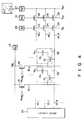
- Fig. 4 illustrates a semiconductor memory device according to the third embodiment of the present invention.
- reference numerals 28 to 30 indicate MOS transistors
- numeral 31 denotes a bonding pad.
- the third embodiment is a modification of the second embodiment and is very effective in preventing the reliability of the semiconductor memory device from being degraded in its normal operation. More specifically, the drains of MOS transistors (second MOS transistors) 28 to 30 are connected to the sources of MOS transistors (first MOS transistors) 23 to 25, respectively. The gates of MOS transistors 28 to 30 are connected in common to one another and are connected to bonding pad 31 which is not used in the normal operation. The sources of MOS transistors 28 to 30 are connected in common to one another and are connected to bonding pad 27 which is also not used in the normal operation.
- gate voltage V G1 applied to bonding pad 26 and gate voltage V G2 applied to bonding pad 31 are set to be not less than V ST + V TH2 (V TH2 represents threshold voltages of MOS transistors 23-25 and 28-30).
- V TH2 represents threshold voltages of MOS transistors 23-25 and 28-30.
- power supply voltage V cc is applied to bonding pad 26 as gate voltage V G1
- voltage V SS e.g., ground voltage
- This situation is realized, for example, by connecting node V G1 to a power supply level (Vcc), node V G2 and V S to a ground level (Vss), respectively, through very high resistive elements.
- the drains of MOS transistors 28 to 30 are thus charged with V CC - VTH2 and, in other words, the potential of V CC - V TH2 is applied to the gate oxide films of MOS transistors 28 to 30 when V SS is a ground voltage, in the normal operation. Further, the voltage of V BOOT (potential of a selected word line) - V CC is applied to the gate oxide films of MOS transistors 23 to 25. It is therefore possible to solve the problem wherein the reliability of the device might be degraded in the normal operation. Since a voltage applied to the gate oxide films of MOS transistors 23 to 25 connected to non-selected word lines is V CC , there is no problem of the degradation of the reliability.
- the semiconductor memory devices according to the second and third embodiments have the same effects as obtained from the semiconductor memory device according to the first embodiment.
- MOS transistors 23-25 and 28-30 are determined so that, even though a stress may destroy a gate insulator film in a particular word line and a leakage decreases the level of voltage on the word line, a voltage applied to the other word lines cannot be influenced. Even if one portion of a gate insulator film is destroyed, the stress to the other part can be still accelerated.
- a predetermined voltage is applied from a bonding pad which is not used in the normal operation mode.
- the bonding pad can be replaced with a bonding pad which is used in the normal operation mode by providing a means for switching its function between the normal operation mode and the stress application mode.
- bonding pads used for the screening test can be shared by plural chips or shared by all the chips on a wafer.
- all the word lines may be driven at once in the screening test.
- a select number of word lines whose number is not less than that of the word lines selected in the normal operation mode can be driven at once.
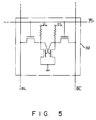
- memory cell 32 of the DRAM can be replaced with a memory cell of the SRAM.
- Two bit lines BL, BL are usually connected to one SRAM cell and they can be connected to signal line V BL through transistor 14 (shown in Figs. 1, 2 and 4) for precharging the bit line.
Landscapes
- For Increasing The Reliability Of Semiconductor Memories (AREA)
- Dram (AREA)
- Semiconductor Memories (AREA)
Claims (19)
- Mémoire à semiconducteurs, comportant :a) une pluralité de cellules de mémoire (15, 16 ; 32) ;b) une pluralité de lignes de transmission de bits (BLn) disposées de telle sorte que chacune desdites cellules de mémoire (15, 16 ; 32) soit couplée à au moins une ligne de transmission de bits (BLn) ;c) une pluralité de premières lignes de transmission de mots (WLOm) ;d) une pluralité de secondes lignes de transmission de mots (WLn) disposées de telle sorte que chacune desdites cellules de mémoire (15, 16 ; 32) est connectée à l'une desdites secondes lignes de transmission de mots (WLn) et au moins l'une desdites secondes lignes de transmission de mots (WLn) est couplée à l'une desdites premières lignes de transmission de mots (WLOm) ;e) des moyens de sélection (1-8) sensibles à des données d'adresse (A₀-An) pour sélectionner l'une desdites premières lignes de transmission de mots (WLOm) et ladite au moins une desdites secondes lignes de transmission de mots (WLn) ; etf) des moyens de commande (22, 31) pour commander lesdites lignes sélectionnées desdites premières et secondes lignes de transmission de mots (WLOm ; WLn) ;g) lesdits moyens de sélection comprenant :
des premiers transistors MOS (1-4) dont les grilles reçoivent des signaux de sélection, dont les sources sont couplées auxdits moyens de commande (22, 31) et dont les drains sont respectivement couplés auxdites premières lignes de transmission de mots (WLOm) ; et
des seconds transistors MOS (5-8) dont les grilles reçoivent des signaux de sélection, dont les sources sont couplées à l'une desdites premières lignes de transmission de mots (WLOm) et dont les drains sont respectivement couplés auxdites secondes lignes de transmission de mots (WLn) ; eth) lesdits moyens de commande (22, 31) comprenant une première source de tension (18, 22) suffisante pour commander la totalité desdites premières et secondes lignes de transmission de mots (WLOm ; WLn) durant une opération d'essai pour détecter un fonctionnement erroné de cellules de mémoire (15, 16 ; 32) de ladite mémoire à semiconducteurs. - Mémoire à semiconducteurs selon la revendication 1, dans laquelle ladite mémoire est une mémoire à accès sélectif dynamique.
- Mémoire à semiconducteurs selon la revendication 1, dans laquelle ladite mémoire est une mémoire à accès sélectif statique.
- Mémoire à semiconducteurs selon la revendication 1, dans laquelle ladite première source de tension (18, 22) comporte un bloc terminal de tension (18) couplé à ladite première pluralité de lignes de transmission de mots (WLOm).
- Mémoire à semiconducteurs selon la revendication 4, dans laquelle une tension continue est appliquée audit bloc terminal de tension (18).
- Mémoire à semiconducteurs selon la revendication 4, dans laquelle une tension alternative est appliquée audit bloc terminal de tension (18).
- Mémoire à semiconducteurs selon la revendication 1, dans laquelle ladite pluralité de lignes de transmission de bits (BLi) est couplée à une seconde source de tension (VBL, 19).
- Mémoire à semiconducteurs selon la revendication 7, dans laquelle ladite seconde source de tension (VBL) comporte un bloc terminal de tension (19).
- Mémoire à semiconducteurs, comportant :a)une pluralité de cellules de mémoire (15, 16 ; 32) ;b) une pluralité de lignes de transmission de mots (WLi, WLj, WLk), chaque ligne de transmission de mots (WLi, WLj, WLk) étant couplée à une pluralité de cellules de mémoire (15, 16 ; 32) ;c) une pluralité de lignes de transmission de bits (BLn), chaque ligne de transmission de bits étant couplée à une pluralité de cellules de mémoire (15, 16; 32) ;d) des moyens de commande (33) couplés à une première extrémité de chacune de ladite pluralité de lignes de transmission de mots (WLi, WLj, WLk) pour commander au moins l'une desdites lignes de transmission de mots (WLi, WLj, WLk) ;e) une pluralité de premiers transistors MOS (23-25) ayant leurs drains respectivement couplés aux secondes extrémités de ladite pluralité de lignes de transmission de mots (WLi, WLj, WLk) et ayant leurs grilles respectives réunies les unes aux autres ; etf) une pluralité de seconds transistors MOS (28-30) ayant leurs drains respectivement couplés aux sources de ladite pluralité de premiers transistors MOS (23-25), ayant leurs grilles respectives réunies les unes aux autres et ayant leurs sources respectives couplées à une première source de tension (27, Vs).
- Mémoire à semiconducteurs selon la revendication 9, dans laquelle ladite première source de tension (27, Vs) comporte une source de tension (Vs) suffisante pour commander simultanément la totalité desdites lignes de transmission de mots (WLi, WLj, WLk).
- Mémoire à semiconducteurs selon la revendication 9, dans laquelle ladite première source de tension (Vs) est une source de tension continue.
- Mémoire à semiconducteurs selon la revendication 9, dans laquelle ladite première source de tension (Vs) est une source de tension alternative.
- Mémoire à semiconducteurs selon la revendication 9, dans laquelle ladite mémoire est une mémoire à accès sélectif dynamique.
- Mémoire à semiconducteurs selon la revendication 9, dans laquelle ladite mémoire est une mémoire à accès sélectif statique.
- Mémoire à semiconducteurs selon la revendication 9, dans laquelle ladite première source de tension (27, Vs) comporte un bloc terminal de tension (27) couplé à ladite pluralité de lignes de transmission de mots (WLi, WLj, WLk).
- Mémoire à semiconducteurs selon la revendication 9, dans laquelle ladite pluralité de lignes de transmission de bits (BLi) est couplée à une seconde source de tension (VBL, 19).
- Mémoire à semiconducteurs selon la revendication 16, dans laquelle ladite seconde source de tension comporte un bloc terminal de tension (19).
- Mémoire à semiconducteurs selon la revendication 9, dans laquelle lesdites grilles respectives de ladite pluralité de premiers transistors MOS (23-25) sont couplées à un bloc terminal de tension (26).
- Mémoire à semiconducteurs selon la revendication 18, dans laquelle lesdites grilles respectives de ladite pluralité de seconds transistors MOS (28-30) sont couplées à un bloc terminal de tension (31).
Applications Claiming Priority (2)
| Application Number | Priority Date | Filing Date | Title |
|---|---|---|---|
| JP1169631A JP2558881B2 (ja) | 1989-06-30 | 1989-06-30 | 半導体メモリ装置 |
| JP169631/89 | 1989-06-30 |
Publications (3)
| Publication Number | Publication Date |
|---|---|
| EP0405576A2 EP0405576A2 (fr) | 1991-01-02 |
| EP0405576A3 EP0405576A3 (en) | 1991-11-27 |
| EP0405576B1 true EP0405576B1 (fr) | 1995-06-07 |
Family
ID=15890080
Family Applications (1)
| Application Number | Title | Priority Date | Filing Date |
|---|---|---|---|
| EP90112452A Expired - Lifetime EP0405576B1 (fr) | 1989-06-30 | 1990-06-29 | Dispositif de mémoire à semi-conducteur |
Country Status (4)
| Country | Link |
|---|---|
| EP (1) | EP0405576B1 (fr) |
| JP (1) | JP2558881B2 (fr) |
| KR (1) | KR940007945B1 (fr) |
| DE (1) | DE69019879T2 (fr) |
Families Citing this family (8)
| Publication number | Priority date | Publication date | Assignee | Title |
|---|---|---|---|---|
| JPH07123134B2 (ja) * | 1990-12-27 | 1995-12-25 | 株式会社東芝 | 半導体装置 |
| JPH0536298A (ja) * | 1991-08-02 | 1993-02-12 | Nec Corp | 半導体記憶装置 |
| JP2793427B2 (ja) * | 1992-04-08 | 1998-09-03 | 株式会社東芝 | 半導体装置 |
| JP3105078B2 (ja) * | 1992-06-12 | 2000-10-30 | 株式会社東芝 | 半導体記憶装置 |
| US5424988A (en) * | 1992-09-30 | 1995-06-13 | Sgs-Thomson Microelectronics, Inc. | Stress test for memory arrays in integrated circuits |
| JP2885597B2 (ja) * | 1993-03-10 | 1999-04-26 | 株式会社東芝 | 半導体メモリ |
| JP3016998B2 (ja) * | 1993-09-24 | 2000-03-06 | 日本電気株式会社 | 半導体記憶装置 |
| JP2009121835A (ja) * | 2007-11-12 | 2009-06-04 | Keithley Instruments Inc | 多チャンネル・パルス試験方法 |
Family Cites Families (7)
| Publication number | Priority date | Publication date | Assignee | Title |
|---|---|---|---|---|
| JPS5925319B2 (ja) * | 1977-04-22 | 1984-06-16 | 三菱電機株式会社 | 半導体メモリ装置 |
| JPS5622278A (en) * | 1979-07-27 | 1981-03-02 | Fujitsu Ltd | Decoder selection system |
| JPS6035760B2 (ja) * | 1980-12-18 | 1985-08-16 | 富士通株式会社 | 半導体記憶装置 |
| EP0101107A2 (fr) * | 1982-07-19 | 1984-02-22 | Motorola, Inc. | Méthode de test d'une mémoire matricielle à semi-conducteur |
| US4816757A (en) * | 1985-03-07 | 1989-03-28 | Texas Instruments Incorporated | Reconfigurable integrated circuit for enhanced testing in a manufacturing environment |
| JPS6452300A (en) * | 1987-08-24 | 1989-02-28 | Hitachi Ltd | Semiconductor memory device |
| JPH01113999A (ja) * | 1987-10-28 | 1989-05-02 | Toshiba Corp | 不揮発性メモリのストレステスト回路 |
-
1989
- 1989-06-30 JP JP1169631A patent/JP2558881B2/ja not_active Expired - Fee Related
-
1990
- 1990-06-29 EP EP90112452A patent/EP0405576B1/fr not_active Expired - Lifetime
- 1990-06-29 DE DE69019879T patent/DE69019879T2/de not_active Expired - Fee Related
- 1990-06-30 KR KR1019900009892A patent/KR940007945B1/ko not_active Expired - Fee Related
Also Published As
| Publication number | Publication date |
|---|---|
| DE69019879T2 (de) | 1995-11-30 |
| JPH0335491A (ja) | 1991-02-15 |
| EP0405576A3 (en) | 1991-11-27 |
| JP2558881B2 (ja) | 1996-11-27 |
| KR910001761A (ko) | 1991-01-31 |
| EP0405576A2 (fr) | 1991-01-02 |
| DE69019879D1 (de) | 1995-07-13 |
| KR940007945B1 (ko) | 1994-08-29 |
Similar Documents
| Publication | Publication Date | Title |
|---|---|---|
| US5258954A (en) | Semiconductor memory including circuitry for driving plural word lines in a test mode | |
| US6307796B1 (en) | Dynamic random access memory | |
| US5615164A (en) | Latched row decoder for a random access memory | |
| US5590079A (en) | Wafer burn-in test circuit of a semiconductor memory device | |
| KR960002010B1 (ko) | 반도체 기억 장치 | |
| KR100329328B1 (ko) | 반도체기억장치 | |
| KR950014099B1 (ko) | 반도체 기억장치 | |
| US4751679A (en) | Gate stress test of a MOS memory | |
| US5619460A (en) | Method of testing a random access memory | |
| US5265057A (en) | Semiconductor memory | |
| EP0492609B1 (fr) | Dispositif à semi-conducteur comprenant des plages de test en tension élevée | |
| US5265056A (en) | Signal margin testing system for dynamic RAM | |
| US5568436A (en) | Semiconductor device and method of screening the same | |
| EP0492610B1 (fr) | RAM dynamique | |
| US5790465A (en) | Wafer burn-in test circuit and a method thereof | |
| EP0405576B1 (fr) | Dispositif de mémoire à semi-conducteur | |
| US6631092B2 (en) | Semiconductor memory device capable of imposing large stress on transistor | |
| CN1121693C (zh) | 半导体存储装置及其测试方法 | |
| US5371710A (en) | Semiconductor memory device having test mode | |
| EP0434904A2 (fr) | Système de test de marge de signal |
Legal Events
| Date | Code | Title | Description |
|---|---|---|---|
| PUAI | Public reference made under article 153(3) epc to a published international application that has entered the european phase |
Free format text: ORIGINAL CODE: 0009012 |
|
| 17P | Request for examination filed |
Effective date: 19900629 |
|
| AK | Designated contracting states |
Kind code of ref document: A2 Designated state(s): DE FR GB |
|
| PUAL | Search report despatched |
Free format text: ORIGINAL CODE: 0009013 |
|
| AK | Designated contracting states |
Kind code of ref document: A3 Designated state(s): DE FR GB |
|
| 17Q | First examination report despatched |
Effective date: 19931129 |
|
| GRAA | (expected) grant |
Free format text: ORIGINAL CODE: 0009210 |
|
| AK | Designated contracting states |
Kind code of ref document: B1 Designated state(s): DE FR GB |
|
| REF | Corresponds to: |
Ref document number: 69019879 Country of ref document: DE Date of ref document: 19950713 |
|
| ET | Fr: translation filed | ||
| PLBE | No opposition filed within time limit |
Free format text: ORIGINAL CODE: 0009261 |
|
| STAA | Information on the status of an ep patent application or granted ep patent |
Free format text: STATUS: NO OPPOSITION FILED WITHIN TIME LIMIT |
|
| 26N | No opposition filed | ||
| PGFP | Annual fee paid to national office [announced via postgrant information from national office to epo] |
Ref country code: FR Payment date: 19970610 Year of fee payment: 8 |
|
| PGFP | Annual fee paid to national office [announced via postgrant information from national office to epo] |
Ref country code: DE Payment date: 19970704 Year of fee payment: 8 |
|
| REG | Reference to a national code |
Ref country code: GB Ref legal event code: 746 Effective date: 19981010 |
|
| PG25 | Lapsed in a contracting state [announced via postgrant information from national office to epo] |
Ref country code: FR Free format text: LAPSE BECAUSE OF NON-PAYMENT OF DUE FEES Effective date: 19990226 |
|
| PG25 | Lapsed in a contracting state [announced via postgrant information from national office to epo] |
Ref country code: DE Free format text: LAPSE BECAUSE OF NON-PAYMENT OF DUE FEES Effective date: 19990401 |
|
| REG | Reference to a national code |
Ref country code: FR Ref legal event code: ST |
|
| REG | Reference to a national code |
Ref country code: GB Ref legal event code: IF02 |
|
| PGFP | Annual fee paid to national office [announced via postgrant information from national office to epo] |
Ref country code: GB Payment date: 20060628 Year of fee payment: 17 |
|
| GBPC | Gb: european patent ceased through non-payment of renewal fee |
Effective date: 20070629 |
|
| PG25 | Lapsed in a contracting state [announced via postgrant information from national office to epo] |
Ref country code: GB Free format text: LAPSE BECAUSE OF NON-PAYMENT OF DUE FEES Effective date: 20070629 |