EP0405800A2 - Assemblage d'un laser et d'un photodétecteur - Google Patents
Assemblage d'un laser et d'un photodétecteur Download PDFInfo
- Publication number
- EP0405800A2 EP0405800A2 EP90306544A EP90306544A EP0405800A2 EP 0405800 A2 EP0405800 A2 EP 0405800A2 EP 90306544 A EP90306544 A EP 90306544A EP 90306544 A EP90306544 A EP 90306544A EP 0405800 A2 EP0405800 A2 EP 0405800A2
- Authority
- EP
- European Patent Office
- Prior art keywords
- laser
- photodetector
- channels
- comprised
- inp
- Prior art date
- Legal status (The legal status is an assumption and is not a legal conclusion. Google has not performed a legal analysis and makes no representation as to the accuracy of the status listed.)
- Ceased
Links
Images

Classifications
-
- H—ELECTRICITY
- H01—ELECTRIC ELEMENTS
- H01S—DEVICES USING THE PROCESS OF LIGHT AMPLIFICATION BY STIMULATED EMISSION OF RADIATION [LASER] TO AMPLIFY OR GENERATE LIGHT; DEVICES USING STIMULATED EMISSION OF ELECTROMAGNETIC RADIATION IN WAVE RANGES OTHER THAN OPTICAL
- H01S5/00—Semiconductor lasers
- H01S5/02—Structural details or components not essential to laser action
- H01S5/026—Monolithically integrated components, e.g. waveguides, monitoring photo-detectors, drivers
- H01S5/0262—Photo-diodes, e.g. transceiver devices, bidirectional devices
- H01S5/0264—Photo-diodes, e.g. transceiver devices, bidirectional devices for monitoring the laser-output
-
- H—ELECTRICITY
- H01—ELECTRIC ELEMENTS
- H01S—DEVICES USING THE PROCESS OF LIGHT AMPLIFICATION BY STIMULATED EMISSION OF RADIATION [LASER] TO AMPLIFY OR GENERATE LIGHT; DEVICES USING STIMULATED EMISSION OF ELECTROMAGNETIC RADIATION IN WAVE RANGES OTHER THAN OPTICAL
- H01S5/00—Semiconductor lasers
- H01S5/20—Structure or shape of the semiconductor body to guide the optical wave ; Confining structures perpendicular to the optical axis, e.g. index or gain guiding, stripe geometry, broad area lasers, gain tailoring, transverse or lateral reflectors, special cladding structures, MQW barrier reflection layers
- H01S5/22—Structure or shape of the semiconductor body to guide the optical wave ; Confining structures perpendicular to the optical axis, e.g. index or gain guiding, stripe geometry, broad area lasers, gain tailoring, transverse or lateral reflectors, special cladding structures, MQW barrier reflection layers having a ridge or stripe structure
- H01S5/227—Buried mesa structure ; Striped active layer
- H01S5/2275—Buried mesa structure ; Striped active layer mesa created by etching
- H01S5/2277—Buried mesa structure ; Striped active layer mesa created by etching double channel planar buried heterostructure [DCPBH] laser
Definitions
- This invention relates generally to lasers and more particularly to a semiconductor injection laser integrated on a wafer together with a monitoring detector.
- Semiconductor injection lasers are used as light sources in long-haul optical fiber transmission system where the information which is transmitted is in the form of an encoded light beam which propagates through a glass fiber.
- the encoded light beam is generated by modulating the current injected into the laser.
- the intensity of the transmitted light beam must be maintained within a specific allowable range. This is usually accomplished by measuring the power output of the laser with a monitoring photodetector which is physically separate from the laser.
- the monitoring detector measures the average power output of the laser.
- the signal from the monitoring detector acting through a feedback circuit, adjusts the injection current of the laser to maintain the average power output of the laser within the allowable range. This adjustment is necessary because the output power may change slowly during operation as a result of slow degradation and/or as a result of variations of the ambient temperature.
- the output power of a laser is measured by diverting a portion of the generated optical power to a separate optical detector. While a separate detector is adequate, it is desirable to have a photodetector which is integrated with the semiconductor injection laser in the same semiconductor chip. Integration of a laser with a photodetector on the same chip can result in a compact laser-photodetector device which has a reduced size, operates with increased speed, provides high performance and has good reliability - all at a lower cost.
- the photodetector can monitor the output power of the laser without substantially degrading the performance of the laser.
- Semiconductor injection lasers are used as sources of optical energy in long-haul optical fiber transmission systems where the information that is being transmitted is represented by encoded light beams which propagate through glass fibers.
- the encoded light beams are generated by modulating the current which is injected into the laser.
- the intensity of the transmitted light should be maintained within a predetermined range. This is normally accomplished by diverting some of the light from the laser to a monitoring photodetector.
- the monitoring photodetector measures the average power output of the laser.
- the signal generated by the photodetector is used to control a feedback circuit which is coupled to adjust the injection current to the laser to keep the average power output of the laser within the predetermined range. This control of the output power of the laser is necessary because the output power can change slowly over a period of time as a result of aging or slow degradation of the laser or by variations of ambient temperature.
- a new improved laser-photodetector structure where the laser and the photodetector are positioned side-by-side and the laser mirrors are formed by cleaving as opposed to etched facets.
- the side-by-side relationship of the laser-photodetector enables the photodetector to monitor the output power of the laser without requiring that a small portion of the output power be diverted to the photodetector.
- Cleaved facets are preferred because etched facets generally have lower reflectivities which result in higher threshold currents and lower external differential quantum efficiencies than for cleaved mirror lasers.
- FIG. 1 there is illustrated a schematic side view of structure in accordance with the principles of the invention.
- the structure is fabricated by depositing four layers by epitaxy growth techniques such as liquid phase epitaxy to an n-InP substrate 10 to form a wafer, for example, as follows: nInP buffer layer 12, an undoped InGaAsP active layer 14; a pin cladding layer 16; and a p-InGaAsP contact layer 18.
- Two channels are then etched on the wafer substantially parallel to the (110) direction using a wet or dry chemical etchant and a dielectric mask such as a SiO2 mask which is deposited using photolithographic techniques.
- Fe-doped semi-insulating InP layers 20 or Ti-doped semi-insulating layers 20 can then be selectively grown only in the two channels by metal organic chemical vapor deposition (MOCVD) growth techniques.
- MOCVD metal organic chemical vapor deposition
- the presence of the mask prevents nucleation and hence the growth of InP in regions outside of the channel.
- the wafer is then processed to provide a laser in one channel and a photodetector in the other channel using standard metallization and photolithographic techniques.
- the final device is an integrated laser-photodetector chip.
- the laser and the photodetector in the structure illustrated in FIG. 1 are positioned "side-by-side".
- the confinement of the current to the active region in the laser section is provided by dielectric 22 deposited on the contact layer 18 and by the semi-insulating layer 20 located in the channels.
- the undoped InGaAsP layer 14 which is bounded by the p-type and n-type InI' cladding layers 16,12 services as both the light emitting region (active region) for the laser and absorbing region for the photodetector.
- the laser contact 24 and photodetector 26 on the p-side are isolated by a layer 28 of SiO2.
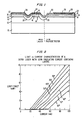
- the light vs. current characteristics of a double channel planar buried heterostructure laser with semi-insulating current confining layer at different temperatures are illustrated in FIG. 2.
- Typical threshold currents are in the range of 20-30 mA at 30 °C. This is comparable to the values observed in other types of strongly index guided laser structures.
- the frequency response characteristics of the laser were found to be unaffected by the presence of the photodetector. Thus, it appears that the semi-insulating layer and the SiO2 layer provide good insulation between the laser and the photodetector.
- FIG. 3 illustrates the measured photodetector current as a function of the current in the laser section (dotted line); and, for comparison, the light output of the laser (solid line).
- the photodetector current increases rapidly up to threshold and then increases slowly. The rapid increase below threshold is caused by absorbed spontaneous emission generated in the active region of the laser. Above threshold, the increase in photodetector current is principally due to scattered stimulated emission.
- the responsitivity of the photodetector can be expressed by the change in photodetector current per unit change in the stimulated light output from the facet.
- the measured responsivity is approximately 78 ⁇ A/ mw
- FIG. 4 illustrates ac coupled photodetector current as a function of pulsed injection
- the laser is biased GW near threshold.
- the ac coupling eliminates the large below-threshold spontaneous emission induced photodetector current shown in FIG. 3.
- FIG. 4 shows that photodetector current follows linearly the stimulated light output from the laser facet.
- detector current can be used to monitor the output of a laser.
- the laser and photodetector sections can be isolated from each other by Fe or Ti doped semi-insulating layers of InP.
- the performance of the laser is comparable to other types of strongly index-guided lasers which do not have a photodetector; and, the photodetector current tracks the laser output power.
- a portion of the electromagnetic energy carried in the evanescent tail of the optical mode is detected by the photodetector for monitoring the average output power of the laser.
- the side-by-side relationship of the laser-photodetector results in a device which, for the first time, can track the laser output power without degrading the laser output power.
- the current from the photodetector can be used to monitor the laser output to provide, with a feedback circuit, stabilization or control of the laser without degrading the output of the laser.
Landscapes
- Physics & Mathematics (AREA)
- Condensed Matter Physics & Semiconductors (AREA)
- General Physics & Mathematics (AREA)
- Electromagnetism (AREA)
- Optics & Photonics (AREA)
- Semiconductor Lasers (AREA)
- Photometry And Measurement Of Optical Pulse Characteristics (AREA)
Applications Claiming Priority (2)
| Application Number | Priority Date | Filing Date | Title |
|---|---|---|---|
| US07/371,474 US4947400A (en) | 1989-06-26 | 1989-06-26 | Laser-photodetector assemblage |
| US371474 | 1989-06-26 |
Publications (2)
| Publication Number | Publication Date |
|---|---|
| EP0405800A2 true EP0405800A2 (fr) | 1991-01-02 |
| EP0405800A3 EP0405800A3 (en) | 1991-05-08 |
Family
ID=23464135
Family Applications (1)
| Application Number | Title | Priority Date | Filing Date |
|---|---|---|---|
| EP19900306544 Ceased EP0405800A3 (en) | 1989-06-26 | 1990-06-15 | Laser-photodetector assemblage |
Country Status (4)
| Country | Link |
|---|---|
| US (1) | US4947400A (fr) |
| EP (1) | EP0405800A3 (fr) |
| JP (1) | JPH0365621A (fr) |
| CA (1) | CA2014937C (fr) |
Cited By (3)
| Publication number | Priority date | Publication date | Assignee | Title |
|---|---|---|---|---|
| EP0507483A1 (fr) * | 1991-04-02 | 1992-10-07 | Lumonics Ltd. | Assemblage de fibres optiques pour un système laser |
| EP0560358A3 (en) * | 1992-03-11 | 1994-05-18 | Sumitomo Electric Industries | Semiconductor laser and process for fabricating the same |
| US8923101B1 (en) | 2013-09-17 | 2014-12-30 | Seagate Technology Llc | Monolithically integrated laser diode and power monitor |
Families Citing this family (11)
| Publication number | Priority date | Publication date | Assignee | Title |
|---|---|---|---|---|
| US5040033A (en) * | 1989-06-26 | 1991-08-13 | At&T Bell Laboratories | Optical amplifier-photodetector assemblage |
| US5252513A (en) * | 1990-03-28 | 1993-10-12 | Xerox Corporation | Method for forming a laser and light detector on a semiconductor substrate |
| US5136604A (en) * | 1990-03-28 | 1992-08-04 | Xerox Corporation | Apparatus and method for detecting the power level in single and multi-stripe integrated lasers |
| US5130762A (en) * | 1990-11-20 | 1992-07-14 | Amp Incorporated | Integrated quantum well feedback structure |
| FR2679388B1 (fr) * | 1991-07-19 | 1995-02-10 | Cit Alcatel | Laser semi-conducteur a double canal et son procede de realisation. |
| US5625636A (en) * | 1991-10-11 | 1997-04-29 | Bryan; Robert P. | Integration of photoactive and electroactive components with vertical cavity surface emitting lasers |
| US5285466A (en) * | 1992-05-20 | 1994-02-08 | Wisconsin Alumni Research Foundation | Feedback mechanism for vertical cavity surface emitting lasers |
| EP0639875A1 (fr) * | 1993-07-12 | 1995-02-22 | BRITISH TELECOMMUNICATIONS public limited company | Structure de barrière électrique pour dispositif semiconducteur |
| JP3535260B2 (ja) * | 1995-05-08 | 2004-06-07 | 三菱電機株式会社 | 半導体光素子並びに該半導体光素子を用いたフォトダイオード、変調器および半導体レーザ |
| US6602629B1 (en) | 2000-05-24 | 2003-08-05 | Eveready Battery Company, Inc. | Zero mercury air cell |
| US11456577B2 (en) * | 2020-07-28 | 2022-09-27 | Raytheon Company | Monolithic quantum cascade laser (QCL)/avalanche photodiode (APD) infrared transceiver |
Family Cites Families (3)
| Publication number | Priority date | Publication date | Assignee | Title |
|---|---|---|---|---|
| US4470143A (en) * | 1981-08-18 | 1984-09-04 | Nippon Electric Co., Ltd. | Semiconductor laser having an etched mirror and a narrow stripe width, with an integrated photodetector |
| JPS61152088A (ja) * | 1984-12-26 | 1986-07-10 | Canon Inc | 半導体レ−ザ |
| JPS6215878A (ja) * | 1985-07-12 | 1987-01-24 | Sharp Corp | 半導体レ−ザ装置 |
-
1989
- 1989-06-26 US US07/371,474 patent/US4947400A/en not_active Expired - Lifetime
-
1990
- 1990-04-19 CA CA002014937A patent/CA2014937C/fr not_active Expired - Lifetime
- 1990-06-15 EP EP19900306544 patent/EP0405800A3/en not_active Ceased
- 1990-06-26 JP JP2165859A patent/JPH0365621A/ja active Pending
Cited By (5)
| Publication number | Priority date | Publication date | Assignee | Title |
|---|---|---|---|---|
| EP0507483A1 (fr) * | 1991-04-02 | 1992-10-07 | Lumonics Ltd. | Assemblage de fibres optiques pour un système laser |
| US5319195A (en) * | 1991-04-02 | 1994-06-07 | Lumonics Ltd. | Laser system method and apparatus for performing a material processing operation and for indicating the state of the operation |
| EP0560358A3 (en) * | 1992-03-11 | 1994-05-18 | Sumitomo Electric Industries | Semiconductor laser and process for fabricating the same |
| US5663975A (en) * | 1992-03-11 | 1997-09-02 | Sumitomo Electric Industries, Ltd. | Multi-beam semiconductor laser with separated contacts characterized by semiconductor mixed crystal and active layer |
| US8923101B1 (en) | 2013-09-17 | 2014-12-30 | Seagate Technology Llc | Monolithically integrated laser diode and power monitor |
Also Published As
| Publication number | Publication date |
|---|---|
| US4947400A (en) | 1990-08-07 |
| JPH0365621A (ja) | 1991-03-20 |
| CA2014937C (fr) | 1994-11-29 |
| EP0405800A3 (en) | 1991-05-08 |
| CA2014937A1 (fr) | 1990-12-26 |
Similar Documents
| Publication | Publication Date | Title |
|---|---|---|
| US6134368A (en) | Optical semiconductor device with a current blocking structure and method for making the same | |
| EP0851548B1 (fr) | Amplificateur optique à semiconducteur | |
| US4947400A (en) | Laser-photodetector assemblage | |
| Nelson et al. | CW electrooptical properties of InGaAsP (λ= 1.3 µm) buried-heterostructure lasers | |
| US5703974A (en) | Semiconductor photonic integrated circuit and fabrication process therefor | |
| US5742423A (en) | Semiconductor optical modulator | |
| US5029297A (en) | Optical amplifier-photodetector device | |
| CA2165711C (fr) | Source lumineuse a semiconducteurs produisant une lumiere tres puissante, a spectre large | |
| CA2014938C (fr) | Ensemble amplificateur optique-photodetecteur | |
| US4939474A (en) | Semiconductor optical amplifier with shortened gain recovery time | |
| US6574258B2 (en) | Semiconductor laser having an active layer provided between two different conduction types of semiconductor layers, and optical modules and communication systems formed therewith | |
| Kasahara et al. | Monolithically integrated high-speed light source using 1.3-µm wavelength DFB-DC-PBH laser | |
| US20050185689A1 (en) | Optoelectronic device having a Discrete Bragg Reflector and an electro-absorption modulator | |
| Botez | Single-mode lasers for optical communications | |
| US5291328A (en) | Semiconductor laser amplifiers | |
| CA1292040C (fr) | Amplificateur optique a semiconducteur a temps retablissement du gain reduit | |
| US5065403A (en) | Self-alignment type window semiconductor laser | |
| US5309469A (en) | Monitoring optical gain of semiconductor optical amplifier | |
| JPH10275960A (ja) | 光半導体素子 | |
| Armistead et al. | Low-threshold ridge waveguide lasers at λ= 1.5 μm | |
| Nobuhara et al. | GRIN-SCH SQW laser/photodiode array by improved microcleaved facet process | |
| Bouadma et al. | GaAs: GaAlAs ridge waveguide lasers and their monolithic integration using the ion beam etching process | |
| Sakakibara et al. | Very narrow spectral linewidth of GaInAs MQW-DFB-PPIBH laser diodes | |
| Motosugi et al. | Single-longitudinal-mode condition for DFB lasers | |
| Dutta et al. | InGaAsP closely spaced dual wavelength laser |
Legal Events
| Date | Code | Title | Description |
|---|---|---|---|
| PUAI | Public reference made under article 153(3) epc to a published international application that has entered the european phase |
Free format text: ORIGINAL CODE: 0009012 |
|
| AK | Designated contracting states |
Kind code of ref document: A2 Designated state(s): DE GB NL |
|
| PUAL | Search report despatched |
Free format text: ORIGINAL CODE: 0009013 |
|
| AK | Designated contracting states |
Kind code of ref document: A3 Designated state(s): DE GB NL |
|
| 17P | Request for examination filed |
Effective date: 19911030 |
|
| 17Q | First examination report despatched |
Effective date: 19920106 |
|
| RAP3 | Party data changed (applicant data changed or rights of an application transferred) |
Owner name: AT&T CORP. |
|
| STAA | Information on the status of an ep patent application or granted ep patent |
Free format text: STATUS: THE APPLICATION HAS BEEN REFUSED |
|
| 18R | Application refused |
Effective date: 19970426 |