EP0405871A2 - Cadre de connexion à capacité équilibrée pour circuits intégrés - Google Patents
Cadre de connexion à capacité équilibrée pour circuits intégrés Download PDFInfo
- Publication number
- EP0405871A2 EP0405871A2 EP90306893A EP90306893A EP0405871A2 EP 0405871 A2 EP0405871 A2 EP 0405871A2 EP 90306893 A EP90306893 A EP 90306893A EP 90306893 A EP90306893 A EP 90306893A EP 0405871 A2 EP0405871 A2 EP 0405871A2
- Authority
- EP
- European Patent Office
- Prior art keywords
- leads
- conductive leads
- integrated circuit
- conductive
- lead frame
- Prior art date
- Legal status (The legal status is an assumption and is not a legal conclusion. Google has not performed a legal analysis and makes no representation as to the accuracy of the status listed.)
- Granted
Links
Images
Classifications
-
- H—ELECTRICITY
- H10—SEMICONDUCTOR DEVICES; ELECTRIC SOLID-STATE DEVICES NOT OTHERWISE PROVIDED FOR
- H10W—GENERIC PACKAGES, INTERCONNECTIONS, CONNECTORS OR OTHER CONSTRUCTIONAL DETAILS OF DEVICES COVERED BY CLASS H10
- H10W70/00—Package substrates; Interposers; Redistribution layers [RDL]
- H10W70/40—Leadframes
- H10W70/411—Chip-supporting parts, e.g. die pads
- H10W70/415—Leadframe inner leads serving as die pads
-
- H—ELECTRICITY
- H10—SEMICONDUCTOR DEVICES; ELECTRIC SOLID-STATE DEVICES NOT OTHERWISE PROVIDED FOR
- H10W—GENERIC PACKAGES, INTERCONNECTIONS, CONNECTORS OR OTHER CONSTRUCTIONAL DETAILS OF DEVICES COVERED BY CLASS H10
- H10W99/00—Subject matter not provided for in other groups of this subclass
-
- H—ELECTRICITY
- H10—SEMICONDUCTOR DEVICES; ELECTRIC SOLID-STATE DEVICES NOT OTHERWISE PROVIDED FOR
- H10W—GENERIC PACKAGES, INTERCONNECTIONS, CONNECTORS OR OTHER CONSTRUCTIONAL DETAILS OF DEVICES COVERED BY CLASS H10
- H10W42/00—Arrangements for protection of devices
-
- H—ELECTRICITY
- H10—SEMICONDUCTOR DEVICES; ELECTRIC SOLID-STATE DEVICES NOT OTHERWISE PROVIDED FOR
- H10W—GENERIC PACKAGES, INTERCONNECTIONS, CONNECTORS OR OTHER CONSTRUCTIONAL DETAILS OF DEVICES COVERED BY CLASS H10
- H10W42/00—Arrangements for protection of devices
- H10W42/20—Arrangements for protection of devices protecting against electromagnetic or particle radiation, e.g. light, X-rays, gamma-rays or electrons
-
- H—ELECTRICITY
- H10—SEMICONDUCTOR DEVICES; ELECTRIC SOLID-STATE DEVICES NOT OTHERWISE PROVIDED FOR
- H10W—GENERIC PACKAGES, INTERCONNECTIONS, CONNECTORS OR OTHER CONSTRUCTIONAL DETAILS OF DEVICES COVERED BY CLASS H10
- H10W72/00—Interconnections or connectors in packages
- H10W72/071—Connecting or disconnecting
- H10W72/073—Connecting or disconnecting of die-attach connectors
-
- H—ELECTRICITY
- H10—SEMICONDUCTOR DEVICES; ELECTRIC SOLID-STATE DEVICES NOT OTHERWISE PROVIDED FOR
- H10W—GENERIC PACKAGES, INTERCONNECTIONS, CONNECTORS OR OTHER CONSTRUCTIONAL DETAILS OF DEVICES COVERED BY CLASS H10
- H10W72/00—Interconnections or connectors in packages
- H10W72/50—Bond wires
- H10W72/551—Materials of bond wires
- H10W72/552—Materials of bond wires comprising metals or metalloids, e.g. silver
- H10W72/5522—Materials of bond wires comprising metals or metalloids, e.g. silver comprising gold [Au]
-
- H—ELECTRICITY
- H10—SEMICONDUCTOR DEVICES; ELECTRIC SOLID-STATE DEVICES NOT OTHERWISE PROVIDED FOR
- H10W—GENERIC PACKAGES, INTERCONNECTIONS, CONNECTORS OR OTHER CONSTRUCTIONAL DETAILS OF DEVICES COVERED BY CLASS H10
- H10W72/00—Interconnections or connectors in packages
- H10W72/50—Bond wires
- H10W72/59—Bond pads specially adapted therefor
-
- H—ELECTRICITY
- H10—SEMICONDUCTOR DEVICES; ELECTRIC SOLID-STATE DEVICES NOT OTHERWISE PROVIDED FOR
- H10W—GENERIC PACKAGES, INTERCONNECTIONS, CONNECTORS OR OTHER CONSTRUCTIONAL DETAILS OF DEVICES COVERED BY CLASS H10
- H10W72/00—Interconnections or connectors in packages
- H10W72/851—Dispositions of multiple connectors or interconnections
- H10W72/853—On the same surface
- H10W72/865—Die-attach connectors and bond wires
-
- H—ELECTRICITY
- H10—SEMICONDUCTOR DEVICES; ELECTRIC SOLID-STATE DEVICES NOT OTHERWISE PROVIDED FOR
- H10W—GENERIC PACKAGES, INTERCONNECTIONS, CONNECTORS OR OTHER CONSTRUCTIONAL DETAILS OF DEVICES COVERED BY CLASS H10
- H10W72/00—Interconnections or connectors in packages
- H10W72/90—Bond pads, in general
- H10W72/941—Dispositions of bond pads
- H10W72/944—Dispositions of multiple bond pads
- H10W72/9445—Top-view layouts, e.g. mirror arrays
-
- H—ELECTRICITY
- H10—SEMICONDUCTOR DEVICES; ELECTRIC SOLID-STATE DEVICES NOT OTHERWISE PROVIDED FOR
- H10W—GENERIC PACKAGES, INTERCONNECTIONS, CONNECTORS OR OTHER CONSTRUCTIONAL DETAILS OF DEVICES COVERED BY CLASS H10
- H10W74/00—Encapsulations, e.g. protective coatings
-
- H—ELECTRICITY
- H10—SEMICONDUCTOR DEVICES; ELECTRIC SOLID-STATE DEVICES NOT OTHERWISE PROVIDED FOR
- H10W—GENERIC PACKAGES, INTERCONNECTIONS, CONNECTORS OR OTHER CONSTRUCTIONAL DETAILS OF DEVICES COVERED BY CLASS H10
- H10W90/00—Package configurations
- H10W90/701—Package configurations characterised by the relative positions of pads or connectors relative to package parts
- H10W90/731—Package configurations characterised by the relative positions of pads or connectors relative to package parts of die-attach connectors
- H10W90/736—Package configurations characterised by the relative positions of pads or connectors relative to package parts of die-attach connectors between a chip and a stacked lead frame, conducting package substrate or heat sink
-
- H—ELECTRICITY
- H10—SEMICONDUCTOR DEVICES; ELECTRIC SOLID-STATE DEVICES NOT OTHERWISE PROVIDED FOR
- H10W—GENERIC PACKAGES, INTERCONNECTIONS, CONNECTORS OR OTHER CONSTRUCTIONAL DETAILS OF DEVICES COVERED BY CLASS H10
- H10W90/00—Package configurations
- H10W90/701—Package configurations characterised by the relative positions of pads or connectors relative to package parts
- H10W90/751—Package configurations characterised by the relative positions of pads or connectors relative to package parts of bond wires
- H10W90/756—Package configurations characterised by the relative positions of pads or connectors relative to package parts of bond wires between a chip and a stacked lead frame, conducting package substrate or heat sink
Definitions
- This invention relates to integrated circuits, and more particularly relates to a lead frame having balanced capacitance for use with integrated circuitry packaging.
- LOC lead on chip
- An integrated circuit is encapsulated in an insulating package, with conductive leads extending from portions of the integrated circuit to the external of the package.
- Each of the conductive leads has substantially the identical capacitance as the remaining conductive leads.
- a lead frame for integrated circuitry which includes a plurality of elongated conductive leads extending in a side-by-side relationship.
- the first ends of the leads are dimensioned to be connected to an integrated circuit and the second ends of the leads are dimensioned to provide electrical connection to external circuits.
- the geometrical area of each of the leads are substantially identical such that the capacitance of each of the leads is substantially identical.
- a lead frame is constructed by providing openings in a sheet of conductive material which define two groups of conductive leads separated by at least one power bus.
- Each group of the conductive leads includes a plurality of elongated leads extending in a side-by-side relationship normally to the power bus.
- the geometrical area of each of the leads is substantially identical such that the capacitance of each of the leads is substantially identical.
- each of the conductive leads has a trapezoidal configuration, the geometric area of the trapezoidal configuration of each of the leads being substantially identical to the remaining leads.
- At least one power bus is associated with the integrated circuitry. Portions of the power bus are oriented adjacent ones of the conductive leads and are provided with substantially identical geometric areas as the conductive leads in order to act as dummy leads to ensure equal capacitance of the remaining leads.
- a conductive layer is disposed adjacent an insulating layer which separates the lead frame and the integrated circuitry in order to provide noise shielding to the integrated circuitry.
- a method of forming an integrated circuit package includes disposing a conductive lead frame adjacent active portions of integrated circuit.
- the conductive lead frame is insulated from the integrated circuit. Portions of the integrated circuit are selectively interconnected with portions of the lead frame.
- the lead frame is configured and oriented such that individual conductive leads have substantially identical capacitances.
- a conductive layer may be provided to provide noise shielding to the integrated circuit.
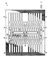
- a lead frame 30 of the present invention comprises a metal sheet which may be formed of, for example, full hard temper CDA alloy 353 which may be approximately. 008 in. in thickness and which may be spot plated in gold, silver, or the like.
- the metal sheet has a plurality of cutouts stamped therein to define a lead configuration.
- the lead configuration comprises a pair of power buses 12 and 14 which comprise elongated parallel conductive lines suitable for receiving electrical power.
- a first group of conductive leads 16 is disposed generally normally to the power bus 12, with leads 16 being arranged in a side-by-side relationship.
- a second group of conductive leads 18 is disposed generally normally to the pover bus 14, with the leads 18 arranged in a side-by-side relationship.
- Conductive leads 16 and 15 are utilized to provide input and output signals to the associated-integrated circuit.
- End portions of power bus 12 extend normally to the center portion of the power bus 12 and are identified as dummy or false leads 20.
- end portions of power bus 14 extend generally normally to the central portion of power bus 14 and are generally identified as dummy or false leads 22.
- Each of the power buses 12 and 14 also include center extensions 24 and 26. As will be subsequently described In greater detail, these center bus extensions 24 and 26 operate as dummy or false conductive leads to assist in maintaining equal capacitance of neighboring conductive leads.
- each of the conductive leads 16 and 18 are formed with a substantially identical geometric configuration. In this way, each of the conductive leads 16 and 18 have substantially identical capacitances.
- Cutouts in the lead frame sheet also define a first group 28 of lead extensions and a second group 30 of lead extensions. As will be subsequently described, these lead extensions 28 and 30 are partially cut or trimmed away during final assembly of the integrated circuit package. Support bars 32 and 34 are provided on opposite ends of the wire frame in order to provide added support to the encapsulated package.
- Locking extensions 32a and 34a are provided to enable locking of the support bars 32 and 34 within the plastic encapsulation to ensure integrity of the package.
- Lead 36 is comprised of three different sections.
- the first section 36a is spaced apart from and oriented normally to the central power bus 12.
- the second or middle portion 36b of the lead is angled away from normal to the power bus 12 and has a trapezoidal cross-sectional area.
- the third section 36c of the lead is disposed normally to the centraL power bus 12.
- section 36a of the lead is used to receive wire bonding to an active portion of the integrated circuit located below the lead.
- Section 36c of the lead extends from the integrated circuit package and is used to make physical contact with exterior circuitry.
- Locking notches 36f are provided in the conductive lead 36 to enable secure locking of the conductive lead within the encapsulation plastic in subsequent encapsulation steps to be described.
- each of the conductive leads 16 and 18 have substantially identical cross-sectional areas as lead 36.
- each of the first sections of the leads which correspond to section 36a are rectangular and have the identical cross-sectional area.
- each of the trapezoidal areas corresponding to section 36b have substantially identical cross-sectional areas.
- each of the mid sections of the conductive leads which form the trapezoidal areas have identical length upper and lower bases which form the trapezoidal area.
- the base 36d of lead 36 is identical in length as the corresponding bases for all other conductive leads on the lead frame.
- the base 36e forming the lower base of the trapezoidaL area has an identical length as all other corresponding bases in the remaining conductive leads. It may also be seen that the heights of the trapezoidal areas of all the conductive leads 16 and 18 are the same. Since trapezoids with equal bases and equal heights have equal areas, the present invention provides an easy technique to ensure that all mid areas of the conductive leads are equal. Similarly, it may be seen that the areas of each of the third sections 36c of the conductive leads are identical. Since the geometrical areas of each of the conductive leads is identical, the capacitance of the leads will be found to be substantially identical.
- An important aspect of the present invention is the provision of the trapezoidal mid-sections of the conductive leads which enable the leads to diverge from normal to accommodate sufficient size external lead pads to ensure adequate electrical contact with exterior circuits.
- the top five conductive leads forming group 16 diverge from normal in an upward angle
- the bottom five conductive leads forming group 16 diverge from normal at a downwardly oriented angle.
- the first five conductive leads forming group 16 diverge from normal at an upward angle
- the bottom five leads diverge from normal at a downward angle.
- the unique geometry of the conductive leads enables this divergence without a change in geometrical area and resulting capacitance.
- Another important aspect of the invention is the provision of the dummy or false leads 20 and 22 as well as the center bus extensions 24 and 26 which form dummy or false leads. Without these dummy or false leads, certain of the conductive leads of the invention could have differing capacitances than their neighbors, because such leads were not surrounded on both sides with identically shaped leads. With the provisions of the identically shaped dummy or false lead extensions 20-26 from the power buses 32 and 34, neighboring conductive leads may be provided with identical capacitances. For example, without dummy or false lead 20, conductive lead 36 would have only its lower neighbor conductive lead closely associated therewith. However, with the provision of the upper dummy lead 20, which is provided with an identical shape to conductive lead 36, lead 36 is surrounded on both sides by identical leads.
- the center bus extensions 24 and 26 operate to provide equal capacitance to their neighbor leads.
- extensions 24 and 26 are of identical construction and each have a Y configuration.
- the Y configuration includes a leg 24a and 24b. It may be seen that each of the legs 24a and 24b are identical in construction and that they have substantially the same trapezoidal configuration as the mid portions of the two adjacent conductive leads.
- the legs 24a and 24b do not extend as far outwardly from power bus 12 as do the conductive leads, since the legs 24a and 24b will not extend outside of the hermetically sealed package.
- Locking notches 24c are provided in each of the legs in order to maintain the substantially identical geometric area, to ensure that the neighboring conductive leads see a substantially identical conductive mass to ensure that substantially identical capacitance is maintained in those adjacent conductive leads.
- the Y shaped configuration of the extensions 24 and 26 enable equal capacitance to be provided to the conductive leads of the invention, even with the diverging orientation of the leads as previously described.
- a small capacitance imbalance may be initially provided because the geometries of the legs 24a and 24b are not identical with those of the neighboring conductive leads.
- this imbalance may be nullified by carefully selecting the length of the legs 24a and 24b to provide the desired exact capacitance balance.
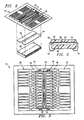
- FIGURE 2 illustrates a perspective exploded view of the connection of the lead frame 10 to an integrated circuit 40.
- Integrated circuit 40 may comprise any suitable type of integrated circuit for use with a lead frame 10, but it has been found particularly advantageous to use the present lead frame with integrated circuits such as DRAMs. In particular, because of the extreme complexity and small dimensions associated with circuits such as the 16 meg DRAM, the present invention is particularly adaptable for use with such complex circuits.
- two pieces of double-sided adhesive 42 and 44 are disposed over the top of the integrated circuit 40 and attach the lead frame 30 over the top of the integrated circuit 40. It is this configuration which leads to the description of the lead over chip (LOC).
- LOC lead over chip
- the use of the double-sided adhesive 42 and 44 is known, and the adhesive may comprise, for example, a double-sided thermosetting epoxy adhesive coated polyimide film which also acts as an active barrier.
- the integrated circuit 40 and the lead frame 10 form a self supporting structure.
- the power buses 12 and 14 and the conductive leads 36 and 38 provide for highly efficient central distribution of voltage, ground and control signals.
- the power buses 32 and 34 and conductive leads 16 and 18 are laminated directly over the primary heat generating circuits of the integrated circuit, thus optimizing heat dissipation.
- FIGURE 3 comprises a top view of the finished subassembly.
- the power buses 12 and 34 comprise spaced apart parallel conductive buses which run along the middle of the integrated circuit 40.
- the adhesives 42 and 44 are spaced apart such that active portions of the integrated circuit 40 are exposed for bonding to the conductive leads of the invention as will be subsequently described.
- the identical configuration of the conductive leads 16 and 18 may be seen, which provides the substantially identical capacitance provided by the invention.
- FIGURES 2 and 3 another important aspect of the invention may be understood. Because of the irregularity of metal disposed over the integrated circuit 40, certain circuits within the integrated circuit 40 are subject to noise. It has been determined that the provision of a conductive layer associated with the adhesives 42 and 44 serves to substantially shield the integrated circuit from the non-uniform leads of the lead frame. In accordance with the invention, a layer of conductive metal such as copper may then be placed on the sides of the adhesives 42 and 44 away from the integrated circuit 40. Adhesive may then be deposited over the metallic layer for connection to the underside of the lead frame 10. Substantial noise shielding is thus provided by the conductive layer associated with the bonding adhesives 42 and 44.
- a conductive metal such as copper may then be placed on the sides of the adhesives 42 and 44 away from the integrated circuit 40. Adhesive may then be deposited over the metallic layer for connection to the underside of the lead frame 10. Substantial noise shielding is thus provided by the conductive layer associated with the bonding adhesives 42 and 44.
- the subassembly is laminated under suitable temperature and pressure conditions and is then oven cured to fully cross-link the adhesive.
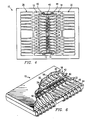
- FIGURE 4 illustrates the next stage of assembly of the present invention wherein high speed thermosonic gold ball wire bonding is accomplished. While it will be understood that various types of wire bonding may be utilized with the invention, bonding using 0.001 in. diameter gold wire has been successfully accomplished. As noted, the gold wire bonds selected portions of the integrated circuit 40 to selected portions of the power buses 12 and 14 and to the conductive leads 16 and 18. For example, wire lead 50 connects the integrated circuit to power bus 12, while wire lead 52 bonds the integrated circuit to one of the conductive leads 16. It will be understood that the wire bonding scheme will vary depending upon the particular configuration of the integrated circuit 40 used with the invention.
- transfer molding of the invention with a molding compound is conducted. While different molding compounds are usable with the present invention, a Novolac epoxy mold compound has been found to work well to encapsulate the entire integrated circuit device. Because of the complexity of the circuitry, low stress mold techniques are utilized. The molded device is then cured, def lashed and lead preparation is conducted on the external leads. The leads are then trimmed and formed by bending to produce the nearly finished product depicted in FIGURES 5 and 6.
- FIGURE 5 illustrates an end view of the substantially finished product wherein the integrated circuit 40 may be seen encapsulated within a plastic body 56.
- Conductive leads 16 and 18 are shown extending from over the integrated circuit 40 and adhesives 42 and 44 to external of the molded plastic body 56. Leads 16 and 18 are bent for suitable physical and electrical contact with external circuitry. Wire bonds 50 and 52 may be seen connecting portions of the integrated circuit 40 with the leads 16 and 18.
- FIGURE 6 illustrates in perspective a partially cut away view of the finished semiconductor package.
- the plastic encapsulation totally surrounds the integrated circuit 40 and all portions of the adhesives 42 and 44.
- FIGURE 6 illustrates clearly the side-by side symmetrical relationships of the lead conductors 16 and 18. It may be seen that the geometry and shape of each of the twenty conductive leads 36 and 38 are substantially identical to one another and that the trapezoidal middle section of the conductive leads enables the leads to diverge from one another while yet maintaining identical geometry. It may also be seen how the dummy or false leads 20-22 act to balance the capacitance of the end conductive leads.
- FIGURE 6 further illustrates the center bus extensions 24 and 26 and shows how the geometry of the Y shaped legs of the extensions 24 and 26 operate as dummy or false leads to balance the capacitance of the diverging neighboring conductive leads.
- the provision of the metallic coating on the adhesive tapes 42 and 44 tends to isolate the elements on the integrated circuit 42 from electrical disturbances in the lead frame 30.
- the resultant symmetry of the present lead frame design and the addition of the dummy or false leads from the power buses improves the thermal dissipation and lowers thermal or temperature gradients of the packaging system, thus allowing a greater number of and more evenly distributed thermal paths.
- An important aspect of the invention is that by balancing the capacitance in the manner described above, the equality of loading capacitance between signal leads is maintained at all lead frame heights above the surface of the integrated circuit 42.
- the conductive leads 16 and 18 may be stepped up or down as needed in order to control the total loading capacitance of the package, while maintaining the equality of capacitance between the individual conductive leads.
- the up or down setting of the leads enables accurate control of the thermal dissipation properties of the package and the stress distribution of the package. The provision of such up or down steps in the conductive leads while maintaining equal capacitance is not available with other designs due to the differing geometries of the neighboring leads.
- a typical width of section 36a may be 0.015 in. while the width of the third section 36c of the conductive lead may comprise .025 in.
- the total length of a conductive lead 16 or 18 in the preferred embodiment may be 0.3 in. The above-noted dimensions have been found to adequately accommodate an integrated package having the dimensions 340 x 660mm.
Landscapes
- Lead Frames For Integrated Circuits (AREA)
- Wire Bonding (AREA)
Priority Applications (1)
| Application Number | Priority Date | Filing Date | Title |
|---|---|---|---|
| EP98122512A EP0917198B1 (fr) | 1989-06-30 | 1990-06-25 | Procédé d'empaquetage d'un dispositif semiconducteur |
Applications Claiming Priority (2)
| Application Number | Priority Date | Filing Date | Title |
|---|---|---|---|
| US37374289A | 1989-06-30 | 1989-06-30 | |
| US373742 | 1995-01-17 |
Related Child Applications (1)
| Application Number | Title | Priority Date | Filing Date |
|---|---|---|---|
| EP98122512A Division EP0917198B1 (fr) | 1989-06-30 | 1990-06-25 | Procédé d'empaquetage d'un dispositif semiconducteur |
Publications (3)
| Publication Number | Publication Date |
|---|---|
| EP0405871A2 true EP0405871A2 (fr) | 1991-01-02 |
| EP0405871A3 EP0405871A3 (en) | 1991-11-27 |
| EP0405871B1 EP0405871B1 (fr) | 1999-09-08 |
Family
ID=23473684
Family Applications (2)
| Application Number | Title | Priority Date | Filing Date |
|---|---|---|---|
| EP19900306893 Expired - Lifetime EP0405871B1 (fr) | 1989-06-30 | 1990-06-25 | Cadre de connexion à capacité équilibrée pour circuits intégrés |
| EP98122512A Expired - Lifetime EP0917198B1 (fr) | 1989-06-30 | 1990-06-25 | Procédé d'empaquetage d'un dispositif semiconducteur |
Family Applications After (1)
| Application Number | Title | Priority Date | Filing Date |
|---|---|---|---|
| EP98122512A Expired - Lifetime EP0917198B1 (fr) | 1989-06-30 | 1990-06-25 | Procédé d'empaquetage d'un dispositif semiconducteur |
Country Status (5)
| Country | Link |
|---|---|
| EP (2) | EP0405871B1 (fr) |
| JP (1) | JPH03102861A (fr) |
| KR (1) | KR0163348B1 (fr) |
| DE (2) | DE69033280T2 (fr) |
| SG (1) | SG49886A1 (fr) |
Cited By (9)
| Publication number | Priority date | Publication date | Assignee | Title |
|---|---|---|---|---|
| EP0409173A3 (en) * | 1989-07-19 | 1991-07-24 | Nec Corporation | Semiconductor ic device having an improved interconnection structure |
| DE4236625A1 (en) * | 1991-10-30 | 1993-05-06 | Mitsubishi Denki K.K., Tokio/Tokyo, Jp | Plastics encapsulated semiconductor device - has resin-filled space above element and under parallel plane in which internal wiring is arranged in proximity to surface electrode connections |
| EP0501830A3 (en) * | 1991-02-28 | 1993-09-22 | Texas Instruments Incorporated | Insulated lead frame for semiconductor packaged devices |
| EP0587112A1 (fr) * | 1992-09-09 | 1994-03-16 | Texas Instruments Incorporated | Cadre conducteur à capacitance réduite pour empaquetage du type conducteur-sur-puce |
| EP0586163A3 (fr) * | 1992-09-02 | 1994-03-23 | Texas Instruments Inc | |
| US5331201A (en) * | 1991-12-24 | 1994-07-19 | Sony Corporation | Semiconductor device having inner lead arrangement with enhanced stability |
| EP0504821A3 (en) * | 1991-03-20 | 1994-11-02 | Hitachi Ltd | Packaged semiconductor device having stress absorbing film |
| EP0758487A4 (fr) * | 1994-05-03 | 1998-09-16 | Douglas W Phelps Jr | Plaque et procede pour soudage sur bande |
| EP0554742B1 (fr) * | 1992-02-03 | 1998-09-30 | Motorola, Inc. | Dispositif semi-conducteur avec connexion-sur-puce |
Families Citing this family (5)
| Publication number | Priority date | Publication date | Assignee | Title |
|---|---|---|---|---|
| KR100259335B1 (ko) * | 1991-12-23 | 2000-09-01 | 김영환 | 리드 온 칩 및 칩 온 리드 구조 패키지 조립방법 |
| JP4256502B2 (ja) | 1998-11-12 | 2009-04-22 | 新光電気工業株式会社 | 半導体装置用リードフレームと半導体装置 |
| KR20020072192A (ko) * | 2001-03-08 | 2002-09-14 | 조통래 | 고체 고분자 전해질 막 및 그의 제조방법 |
| JP2003079295A (ja) * | 2001-09-13 | 2003-03-18 | Daiwa Seiko Inc | 釣り用天秤 |
| JP2005252140A (ja) * | 2004-03-08 | 2005-09-15 | Olympus Corp | 固体撮像装置用パッケージ |
Family Cites Families (4)
| Publication number | Priority date | Publication date | Assignee | Title |
|---|---|---|---|---|
| CA1238119A (fr) * | 1985-04-18 | 1988-06-14 | Douglas W. Phelps, Jr. | Microplaquette conditionee |
| US4684975A (en) * | 1985-12-16 | 1987-08-04 | National Semiconductor Corporation | Molded semiconductor package having improved heat dissipation |
| US4801999A (en) * | 1987-07-15 | 1989-01-31 | Advanced Micro Devices, Inc. | Integrated circuit lead frame assembly containing voltage bussing and distribution to an integrated circuit die using tape automated bonding with two metal layers |
| US4965654A (en) * | 1989-10-30 | 1990-10-23 | International Business Machines Corporation | Semiconductor package with ground plane |
-
1990
- 1990-06-25 EP EP19900306893 patent/EP0405871B1/fr not_active Expired - Lifetime
- 1990-06-25 EP EP98122512A patent/EP0917198B1/fr not_active Expired - Lifetime
- 1990-06-25 DE DE69033280T patent/DE69033280T2/de not_active Expired - Fee Related
- 1990-06-25 SG SG1996008184A patent/SG49886A1/en unknown
- 1990-06-25 DE DE1990634069 patent/DE69034069T2/de not_active Expired - Fee Related
- 1990-06-28 JP JP2171300A patent/JPH03102861A/ja active Pending
- 1990-06-29 KR KR1019900009709A patent/KR0163348B1/ko not_active Expired - Fee Related
Cited By (12)
| Publication number | Priority date | Publication date | Assignee | Title |
|---|---|---|---|---|
| EP0409173A3 (en) * | 1989-07-19 | 1991-07-24 | Nec Corporation | Semiconductor ic device having an improved interconnection structure |
| EP0501830A3 (en) * | 1991-02-28 | 1993-09-22 | Texas Instruments Incorporated | Insulated lead frame for semiconductor packaged devices |
| EP0504821A3 (en) * | 1991-03-20 | 1994-11-02 | Hitachi Ltd | Packaged semiconductor device having stress absorbing film |
| US5406028A (en) * | 1991-03-20 | 1995-04-11 | Hitachi, Ltd. | Packaged semiconductor device having stress absorbing film |
| DE4236625A1 (en) * | 1991-10-30 | 1993-05-06 | Mitsubishi Denki K.K., Tokio/Tokyo, Jp | Plastics encapsulated semiconductor device - has resin-filled space above element and under parallel plane in which internal wiring is arranged in proximity to surface electrode connections |
| DE4236625C2 (de) * | 1991-10-30 | 1997-11-27 | Mitsubishi Electric Corp | Halbleitervorrichtung mit LOC-Leiterrahmen und Verfahren zu ihrer Herstellung |
| US5331201A (en) * | 1991-12-24 | 1994-07-19 | Sony Corporation | Semiconductor device having inner lead arrangement with enhanced stability |
| EP0554742B1 (fr) * | 1992-02-03 | 1998-09-30 | Motorola, Inc. | Dispositif semi-conducteur avec connexion-sur-puce |
| EP0586163A3 (fr) * | 1992-09-02 | 1994-03-23 | Texas Instruments Inc | |
| EP0587112A1 (fr) * | 1992-09-09 | 1994-03-16 | Texas Instruments Incorporated | Cadre conducteur à capacitance réduite pour empaquetage du type conducteur-sur-puce |
| US5521426A (en) * | 1992-09-09 | 1996-05-28 | Texas Instruments Incorporated | Reduced capacitance lead frame for lead on chip package |
| EP0758487A4 (fr) * | 1994-05-03 | 1998-09-16 | Douglas W Phelps Jr | Plaque et procede pour soudage sur bande |
Also Published As
| Publication number | Publication date |
|---|---|
| EP0405871B1 (fr) | 1999-09-08 |
| DE69033280D1 (de) | 1999-10-14 |
| EP0405871A3 (en) | 1991-11-27 |
| SG49886A1 (en) | 1998-06-15 |
| JPH03102861A (ja) | 1991-04-30 |
| DE69034069D1 (de) | 2003-06-12 |
| EP0917198A1 (fr) | 1999-05-19 |
| DE69034069T2 (de) | 2004-04-01 |
| EP0917198B1 (fr) | 2003-05-07 |
| DE69033280T2 (de) | 1999-12-30 |
| KR910001950A (ko) | 1991-01-31 |
| KR0163348B1 (ko) | 1998-12-01 |
Similar Documents
| Publication | Publication Date | Title |
|---|---|---|
| US5233220A (en) | Balanced capacitance lead frame for integrated circuits and integrated circuit device with separate conductive layer | |
| US5432127A (en) | Method for making a balanced capacitance lead frame for integrated circuits having a power bus and dummy leads | |
| US5648679A (en) | Tape ball lead integrated circuit package | |
| US6261865B1 (en) | Multi chip semiconductor package and method of construction | |
| US6555902B2 (en) | Multiple stacked-chip packaging structure | |
| US5483024A (en) | High density semiconductor package | |
| US5677567A (en) | Leads between chips assembly | |
| US5138430A (en) | High performance versatile thermally enhanced IC chip mounting | |
| US6218202B1 (en) | Semiconductor device testing and burn-in methodology | |
| EP0917198B1 (fr) | Procédé d'empaquetage d'un dispositif semiconducteur | |
| US6291881B1 (en) | Dual silicon chip package | |
| KR970006529B1 (ko) | 반도체 장치 | |
| US5227995A (en) | High density semiconductor memory module using split finger lead frame | |
| US20040113256A1 (en) | Stack arrangement of a memory module | |
| US6815746B2 (en) | Semiconductor device and method of manufacturing the same | |
| KR100255476B1 (ko) | 볼 그리드 어레이 패키지 | |
| US5994169A (en) | Lead frame for integrated circuits and process of packaging | |
| US5569955A (en) | High density integrated circuit assembly combining leadframe leads with conductive traces | |
| US5650660A (en) | Circuit pattern for a ball grid array integrated circuit package | |
| GB2272104A (en) | Tape automated bonding | |
| US6794745B1 (en) | Lead on chip type semiconductor package | |
| EP2156468B1 (fr) | Dispositif à semi-conducteurs comportant une couche de redistribution multipuce | |
| JPH0770675B2 (ja) | 半導体装置およびその製造方法 | |
| JPH0318344B2 (fr) | ||
| JPS60187046A (ja) | 半導体装置およびその製造方法 |
Legal Events
| Date | Code | Title | Description |
|---|---|---|---|
| PUAI | Public reference made under article 153(3) epc to a published international application that has entered the european phase |
Free format text: ORIGINAL CODE: 0009012 |
|
| AK | Designated contracting states |
Kind code of ref document: A2 Designated state(s): DE FR GB IT NL |
|
| PUAL | Search report despatched |
Free format text: ORIGINAL CODE: 0009013 |
|
| AK | Designated contracting states |
Kind code of ref document: A3 Designated state(s): DE FR GB IT NL |
|
| 17P | Request for examination filed |
Effective date: 19920511 |
|
| 17Q | First examination report despatched |
Effective date: 19940728 |
|
| GRAG | Despatch of communication of intention to grant |
Free format text: ORIGINAL CODE: EPIDOS AGRA |
|
| GRAG | Despatch of communication of intention to grant |
Free format text: ORIGINAL CODE: EPIDOS AGRA |
|
| GRAH | Despatch of communication of intention to grant a patent |
Free format text: ORIGINAL CODE: EPIDOS IGRA |
|
| GRAH | Despatch of communication of intention to grant a patent |
Free format text: ORIGINAL CODE: EPIDOS IGRA |
|
| GRAA | (expected) grant |
Free format text: ORIGINAL CODE: 0009210 |
|
| AK | Designated contracting states |
Kind code of ref document: B1 Designated state(s): DE FR GB IT NL |
|
| REF | Corresponds to: |
Ref document number: 69033280 Country of ref document: DE Date of ref document: 19991014 |
|
| ET | Fr: translation filed | ||
| PLBE | No opposition filed within time limit |
Free format text: ORIGINAL CODE: 0009261 |
|
| STAA | Information on the status of an ep patent application or granted ep patent |
Free format text: STATUS: NO OPPOSITION FILED WITHIN TIME LIMIT |
|
| 26N | No opposition filed | ||
| REG | Reference to a national code |
Ref country code: GB Ref legal event code: IF02 |
|
| PGFP | Annual fee paid to national office [announced via postgrant information from national office to epo] |
Ref country code: NL Payment date: 20070507 Year of fee payment: 18 |
|
| PGFP | Annual fee paid to national office [announced via postgrant information from national office to epo] |
Ref country code: DE Payment date: 20070629 Year of fee payment: 18 |
|
| PGFP | Annual fee paid to national office [announced via postgrant information from national office to epo] |
Ref country code: GB Payment date: 20070511 Year of fee payment: 18 |
|
| PGFP | Annual fee paid to national office [announced via postgrant information from national office to epo] |
Ref country code: IT Payment date: 20070628 Year of fee payment: 18 |
|
| PGFP | Annual fee paid to national office [announced via postgrant information from national office to epo] |
Ref country code: FR Payment date: 20070605 Year of fee payment: 18 |
|
| GBPC | Gb: european patent ceased through non-payment of renewal fee |
Effective date: 20080625 |
|
| NLV4 | Nl: lapsed or anulled due to non-payment of the annual fee |
Effective date: 20090101 |
|
| REG | Reference to a national code |
Ref country code: FR Ref legal event code: ST Effective date: 20090228 |
|
| PG25 | Lapsed in a contracting state [announced via postgrant information from national office to epo] |
Ref country code: DE Free format text: LAPSE BECAUSE OF NON-PAYMENT OF DUE FEES Effective date: 20090101 |
|
| PG25 | Lapsed in a contracting state [announced via postgrant information from national office to epo] |
Ref country code: NL Free format text: LAPSE BECAUSE OF NON-PAYMENT OF DUE FEES Effective date: 20090101 |
|
| PG25 | Lapsed in a contracting state [announced via postgrant information from national office to epo] |
Ref country code: GB Free format text: LAPSE BECAUSE OF NON-PAYMENT OF DUE FEES Effective date: 20080625 |
|
| PG25 | Lapsed in a contracting state [announced via postgrant information from national office to epo] |
Ref country code: IT Free format text: LAPSE BECAUSE OF NON-PAYMENT OF DUE FEES Effective date: 20080625 Ref country code: FR Free format text: LAPSE BECAUSE OF NON-PAYMENT OF DUE FEES Effective date: 20080630 |