EP0406852A2 - Verfahren und Gerät zur automatischen Pegelregelung in einem optischen Plattensystem - Google Patents
Verfahren und Gerät zur automatischen Pegelregelung in einem optischen Plattensystem Download PDFInfo
- Publication number
- EP0406852A2 EP0406852A2 EP90112842A EP90112842A EP0406852A2 EP 0406852 A2 EP0406852 A2 EP 0406852A2 EP 90112842 A EP90112842 A EP 90112842A EP 90112842 A EP90112842 A EP 90112842A EP 0406852 A2 EP0406852 A2 EP 0406852A2
- Authority
- EP
- European Patent Office
- Prior art keywords
- gain
- value
- signal
- amplitude
- recorded
- Prior art date
- Legal status (The legal status is an assumption and is not a legal conclusion. Google has not performed a legal analysis and makes no representation as to the accuracy of the status listed.)
- Granted
Links
Images

Classifications
-
- H—ELECTRICITY
- H03—ELECTRONIC CIRCUITRY
- H03G—CONTROL OF AMPLIFICATION
- H03G3/00—Gain control in amplifiers or frequency changers
- H03G3/20—Automatic control
- H03G3/30—Automatic control in amplifiers having semiconductor devices
- H03G3/3084—Automatic control in amplifiers having semiconductor devices in receivers or transmitters for electromagnetic waves other than radiowaves, e.g. lightwaves
-
- G—PHYSICS
- G11—INFORMATION STORAGE
- G11B—INFORMATION STORAGE BASED ON RELATIVE MOVEMENT BETWEEN RECORD CARRIER AND TRANSDUCER
- G11B20/00—Signal processing not specific to the method of recording or reproducing; Circuits therefor
- G11B20/10—Digital recording or reproducing
- G11B20/10009—Improvement or modification of read or write signals
- G11B20/10018—Improvement or modification of read or write signals analog processing for digital recording or reproduction
- G11B20/10027—Improvement or modification of read or write signals analog processing for digital recording or reproduction adjusting the signal strength during recording or reproduction, e.g. variable gain amplifiers
-
- G—PHYSICS
- G11—INFORMATION STORAGE
- G11B—INFORMATION STORAGE BASED ON RELATIVE MOVEMENT BETWEEN RECORD CARRIER AND TRANSDUCER
- G11B7/00—Recording or reproducing by optical means, e.g. recording using a thermal beam of optical radiation by modifying optical properties or the physical structure, reproducing using an optical beam at lower power by sensing optical properties; Record carriers therefor
- G11B7/004—Recording, reproducing or erasing methods; Read, write or erase circuits therefor
- G11B7/005—Reproducing
Definitions
- the present invention relates to an automatic gain control method and apparatus in an optical disk system and, more particularly, to automatic gain control method and apparatus which can discriminate whether a data has been recorded in a certain area on an optical disk to record user's data or not.
- each track is divided into a plurality of sectors, and information is recorded or reproduced on a sector unit basis.
- Each sector has a preformat portion in which control information such as identification (ID) and the like has previously been recorded and an information recording portion to record user's data.
- ID identification
- JP-A-60-115073 As an optical disk apparatus having a function to discriminate whether a data has correctly been recorded in the information recording portion or not, for instance, there has been known a technique disclosed in JP-A-60-115073. According to such a technique, an envelope of a reproduction signal of the optical disk is detected, the level of the envelope signal is compared with a reference potential, a time duration of a period when the envelope signal level is deviated from the reference potential is counted, and when the time duration is shorter than the reference time duration it is determined that the data has correctly been recorded.
- an automatic gain control method whereby an amplitude fluctuation of the reproduction signal is compensated to make the amplitude constant has conventionally been well known.
- a gain of an amplifier of the gain controller is increased.
- Another object of the present invention is to prevent the noise and the remaining signal which are not erased when erasing the recorded data from being erroneously recognized as an inherent reproduction signal.
- Still another object of the present invention is to provide an automatic gain control method and apparatus which can accurately recognize whether a data has already been recorded in an area to record user's data or not.
- a second control value to control a gain of a variable gain amplifier is used.
- the second control value increases as the reproduction signal amplitude of the newly recorded information decreases. Even when the reproduction signal amplitude of the newly recorded information slightly decreased, the gain of the variable gain amplifier increases in accordance with the reproduction amplitude reduction and an output of the variable gain amplifier can be made constant.
- the first control value is used. Since the reproduction level of the previously recorded information such as an ID and the like is sufficiently higher than the reproduction level of the newly recorded information, the first control value is sufficiently smaller than the second control value, so that the gain of the variable gain amplifier is suppressed to an extremely small value. Thus, a situation such that the noise and the remaining signal component which was not erased are erroneously recognized as an inherent signal or that the unrecorded portion is erroneously recognized as a recording portion does not occur.
- the first control value increases as the reproduction amplitude of the previously recorded information decreases
- the second control value increases as the reproduction amplitude of the newly recorded information decreases. Therefore, the amplitude difference between the previously recorded information and the newly recorded information corresponds to the difference between the first and second control values and can be discriminated by checking the difference between the first and second control values.
- an automatic gain control apparatus of an optical disk apparatus comprises: first gain control means for controlling a gain of a variable gain amplifier for an information signal which has previously been recorded, for instance, a reproduction signal from a preformat portion of an ID and the like and for setting an amplitude of an output signal of the variable gain amplifier to a predetermined value; a first memory circuit to store a control value which gives the predetermined amplitude as a first control value; second gain control means for controlling the gain of the variable gain amplifier for information which was newly recorded, for instance, a reproduction signal from an area to record user's data and for setting an amplitude of an output signal of the variable gain amplifier to a predetermined value; a second memory circuit to store a control value which gives the predetermined amplitude as a second control value; discriminating means for discriminating whether an amplitude difference between the reproduction signal of the previously recorded information and the reproduction signal of the newly recorded information is equal to or smaller than a predetermined value or not; and control value setting means which is constructed in a manner such
- the discriminating means can be also constructed so as to compare the first and second control values which were stored and to thereby discriminate whether the difference therebetween is equal to or smaller than a predetermined value or not.
- the first and second gain control means can be also constructed by one common gain controller.
- the first and second memory circuits are respectively constructed by, for instance, latch circuits.
- those two memory circuits may be also constructed as a single memory.
- the control value (the first control value) to set the amplifier output amplitude for the previously recorded information to a predetermined value is used as a gain control value of the variable gain amplifier for reproduction, and when the reproduction amplitude difference is out of the predetermined value, the control value (the second control value) to set the amplifier output amplitude for the newly recorded information to a predetermined value is used as the gain control value.
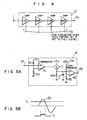
- a reference numeral 1 denotes a light detection reproduction signal
- 2 indicates a variable gain controller (AGC circuit);
- 2a an output signal of the AGC circuit 2;
- 3 an analog/digital (A/D) converter;
- 4 an amplitude detecting circuit;
- 5 a first memory circuit such as a latch circuit;
- 5a a first control value;
- 6 a second memory circuit such as a latch circuit;
- 8 a control logic circuit using, for instance, a microcomputer; and 9 a digital data output.
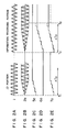
- Fig. 3 shows a sector construction on a track of an optical disk.
- an optical disk which is specified bny the ISO (International Standard Organization)
- one track is divided into a plurality of sectors and each sector is constructed such that an ID portion (for example, six byte length) and a data recording portion are continuously arranged after a sector mark.
- the ID portion is also called a prepit portion or a preformat portion and is a portion in which control information has previously been recorded.
- the subsequent information recording portion is a recording portion to, for instance, magnetooptically record user's data.
- the recording portion of the optical disk is preliminarily magnetized and data is recorded into the magnetized information recording portion by irradiating a laser beam thereto.
- the ID portion is a portion in which necessary control information such as addresses, sync information, and the like has previously been recorded by physically forming pits (namely, holes) into the optical disk.
- a change in light quality of the reflected lights from the pits which are obtained when a light was irradiated onto the optical disk is used as a photo detection signal 1. That is, light quality changes due to the presence or absence of the pits in the ID portion and the signal 1 including the control information is reproduced.
- a rotation amount of the light due to the Kerr rotation by the Kerr effect is detected and used as a photo detection signal 1.
- the ID portion is detected after the elapse of a time T1 (Figs. 2A - 2E) from the detection of the sector mark and the area of the information recording portion is detected after the elapse of time T2.
- the photo detection signal 1 is inputted to the AGC circuit 2 and is amplified in accordance with the gain control value 7a.
- the AGC circuit 2 can increase the gain every dB by 16 steps from 0 dB to 15 dB in accordance with the control value 7a of, e.g., four bits.
- the gain control value 7a was first set to the lowest limit value by the operating circuit 7 at time T1, so that the gain of the AGC circuit 2 was set to the lowest value (e.g., 0 dB). Then, the operating circuit 7 increases the gain control value 7a one step by one at predetermined period (for instance, one-bit period of the reproduction signal 2). Thus, the gain of the AGC circuit 2 is increased one dB by one and the output signal 2a shown in Fig. 2B is obtained from the AGC circuit 2. When the output signal 2a has reached a predetermined amplitude, such a state is detected by the amplitude detecting circuit 4.
- Fig. 5A shows a practical example of the amplitude detecting circuit 4.
- the output signal 2a of the AGC circuit 2 is compared with a predetermined voltage E1 which is divided by resistors R1 and R2.
- a predetermined voltage E1 which is divided by resistors R1 and R2.
- an output of a comparator 41 is set to the low level and a constant current circuit I1 is turned off. Since a voltage level of a + side input of a comparator 42 is lower than a voltage which is divided by resistors R4 and R5, an output 4a of the comparator 42 (namely, an output of the amplitude detecting circuit 4) is set to the low level.
- the output of the comparator 41 When the level of the AGC output signal 2a is larger than the predetermined voltage which is divided by the resistors R1 and R2, the output of the comparator 41 is set to the high level, the constant current circuit I1 is turned on, a capacitor C is charged, and the level of the + side input of the comparator 42 is larger than the - side voltage.
- the output 4a of the comparator 42 i.e., the output of the amplitude detecting circuit 4
- the output 4a of the comparator 42 can be set to the high level.
- the first memory circuit 5 and the operating circuit 7 are made operative by the detection signal, namely, the output 4a of the amplitude detecting circuit 4.
- the gain control value 7a at that time is stored as a first control value 5a into the first memory circuit 5.
- the gain of the AGC circuit 2 is controlled to a desired gain, so that the output signal 2a of a predetermined amplitude is derived. That is, the envelope of the reproduction signal 2a from the ID portion is maintained to a predetermined level.
- the newly recorded information namely, the newly recorded user's data is read out of the information recording portion after time T2.
- the gain control value 7a is separated from the first control value 5a, the gain control value 7a is similarly set to the lowest limit value, and the gain of the AGC circuit 2 is set to the lowest value (for example, 0 dB).
- the gain control value 7a is increased by one step at a predetermined period (e.g., one-bit period) and the gain of the AGC circuit 2 is increased one dB by one.
- the amplitude detecting circuit 4 When the amplitude of the output signal 2a increases and reaches a predetermined amplitude, the amplitude detecting circuit 4 generates the detection output signal 4a in a manner similar to the above.
- the second memory circuit 6 and the operating circuit 7 are made operative by the detection signal 4a and the gain control value 7a at that time is stored as a second control value 6a into the second memory circuit 6.
- the second control value 6a is used as a gain control value 7a to control the gain of the AGC circuit 2 while the information is being reproduced from the subsequent information recording portion, so that the output signal 2a of a predetermined amplitude is derived. That is, the envelope of the reproduction signal 2a of the information recording section which was newly recorded is maintained to a predetermined level.
- the difference between the first and second control values 5a and 6a is calculated by the operating circuit 7.
- the operating circuit 7 detects the difference between the first gain control value 5a to set the amplitude of the reproduction signal, i.e., signal 2a of the ID portion having relatively high reliability to a predetermined value and the second gain control value 6a to set the amplitude of the reproduction signal of the information recording portion whose S/N ratio is lower than that of the ID portion to a predetermined value.
- the difference between the control values 5a and 6a corresponds to the difference between the photo detection reproduction signal 1 from the ID portion and the signal 1 from the information recording portion.
- the difference is transferred to the gain switching control logic circuit 8 comprising, for instance, a microcomputer, if it is determined by the discriminating circuit in the control logic circuit 8 that the difference lies within the predetermined range, that is, when the reproduction level of the data recorded in the information recording portion is not extremely lower than the photo detection signal level of the ID portion, the second control value 6a is set as it is as a gain control value 7a at time T3 and is used after that.
- the second gain control value 6a is set to "6". For instance, when a condition such that (
- the gain control value 7a is switched from the second control value 6a to the first control value 5a at time T3 by the control logic circuit 8 and is set. For instance, when the photo detection signal of the ID portion is larger than the signal of the information recording portion by 3 dB,
- 3, so that the difference is out of the predetermined range in the above condition.
- the value "4" as a first control value 5a is used as a control value 7a.
- the following three methods are considered as a method where the photo detection reproduction signal 1 is outputted from the ID portion and the information recording portion and the AGC is executed to the photo detection reproduction signal 1.
- the first method relates to the case of what is called a "Read After Write” in which after data was recorded into the information recording portion, it is regenerated to check the recording quality of the data.
- the second method relates to the case of what is called “Read After Erase” in which after data was erased, the erasing quality is checked.
- the third method relates to the case of ordinary "Read".
- the gain of the AGC circuit 2 is controlled by using the second control value 6a such that the photo detection reproduction signal from the newly recorded portion (data portion of the information recording portion) is set to a predetermined amplitude after time T3. Therefore, the input (output 2a of the AGC circuit) of the A/D converting circuit 3 which is connected to the AGC circuit 2 becomes stable. The saturation of the circuit due to an excessive amplitude and the influence by the offset voltage due to the too small amplitude are eliminated. The deterioration of the data quality can be prevented.
- the second control value 6a reaches a value near the highest limit value (broken line in Fig. 2D).
- the difference between the second control value 6a and the first control value 5a as a gain control value of the ID portion increases.
- the control value 7a is set to the first control value 5a at time T3. Therefore, since the gain of the AGC circuit 2 corresponding to the unrecorded portion is suppressed to a lower value (than the value when the second control value 6a is used as it is), the noise of the magnetooptic recording portion and the level of the remaining signal which was not erased are also suppressed to enough low values and are not erroneously recognized as the normal signal data. That is, the case where the data has normally been recorded and the case where data is not recorded can be clearly distinguished.
- the case where a data is not recorded can be considered to be the case where the photo detection reproduction signal 1 shown by the broken line in Fig. 2A, extremely decreases. Therefore, the second control value 6a extremely increases and the value of
- the series of gain control operations mentioned above are repeated every sector constructing the track of the optical disk. That is, whenever the sector mark is detected, the gain control value 7a is initialized to the lowest value and the above operations are executed from that timing.
- gain control values 5a and 6a which are stored
- a plurality of control values before them for instance, regarding a few sectors
- the average value or intermediate value of those control values is used or the like (preferably, a function of the gain control value for the reproduction signal of the previous information is used)
- the quality guarantee can be also improved for a detect and the like of the disk.
- the average level of the ID portion in one sector is detected and a desired gain control value corresponding to the average value can be also set to the first control value.
- the memory circuits 5 and 6 in the above embodiment can be also physically constructed by one memory.
- the above embodiment has been described with respect to the reproduction of the information from each sector of the rewritable type optical disk, for instance, magnetooptic disk or the gain control
- the invention can be also applied to an unrewritable type optical disk, for instance, write once type optical disk to which information can be written once.
- the invention is not limited to the optical disk apparatus but can be also applied to other apparatus for optically recording and reproducing information, for instance, an optical card apparatus or the like.
Landscapes
- Engineering & Computer Science (AREA)
- Signal Processing (AREA)
- Physics & Mathematics (AREA)
- Electromagnetism (AREA)
- Optical Recording Or Reproduction (AREA)
- Signal Processing For Digital Recording And Reproducing (AREA)
Applications Claiming Priority (2)
| Application Number | Priority Date | Filing Date | Title |
|---|---|---|---|
| JP1173052A JP2667522B2 (ja) | 1989-07-06 | 1989-07-06 | 光ディスク装置 |
| JP173052/89 | 1989-07-06 |
Publications (3)
| Publication Number | Publication Date |
|---|---|
| EP0406852A2 true EP0406852A2 (de) | 1991-01-09 |
| EP0406852A3 EP0406852A3 (en) | 1993-08-25 |
| EP0406852B1 EP0406852B1 (de) | 1995-01-25 |
Family
ID=15953326
Family Applications (1)
| Application Number | Title | Priority Date | Filing Date |
|---|---|---|---|
| EP90112842A Expired - Lifetime EP0406852B1 (de) | 1989-07-06 | 1990-07-05 | Verfahren und Gerät zur automatischen Pegelregelung in einem optischen Plattensystem |
Country Status (4)
| Country | Link |
|---|---|
| US (1) | US5124967A (de) |
| EP (1) | EP0406852B1 (de) |
| JP (1) | JP2667522B2 (de) |
| DE (1) | DE69016285T2 (de) |
Cited By (1)
| Publication number | Priority date | Publication date | Assignee | Title |
|---|---|---|---|---|
| EP0792016A1 (de) * | 1996-02-26 | 1997-08-27 | Samsung Electronics Co., Ltd. | Signalverarbeitungsvorverstärker für eine Vorrichtung für optische Platte |
Families Citing this family (26)
| Publication number | Priority date | Publication date | Assignee | Title |
|---|---|---|---|---|
| US6141300A (en) | 1989-06-20 | 2000-10-31 | Discovision Associates | Optical actuator including lens assembly with optical axis having symmetric suspensory forces acting thereon and optical disc system including same |
| US5265079A (en) | 1991-02-15 | 1993-11-23 | Applied Magnetics Corporation | Seek actuator for optical recording |
| EP0445780B1 (de) * | 1990-03-07 | 1997-07-09 | Canon Kabushiki Kaisha | System zum Aufzeichnen und Wiedergeben eines Bildsignals |
| JPH0495223A (ja) * | 1990-08-09 | 1992-03-27 | Olympus Optical Co Ltd | 光学式情報記録再生装置 |
| US6069857A (en) | 1991-02-15 | 2000-05-30 | Discovision Associates | Optical disc system having improved circuitry for performing blank sector check on readable disc |
| US5729511A (en) | 1991-02-15 | 1998-03-17 | Discovision Associates | Optical disc system having servo motor and servo error detection assembly operated relative to monitored quad sum signal |
| US5677899A (en) | 1991-02-15 | 1997-10-14 | Discovision Associates | Method for moving carriage assembly from initial position to target position relative to storage medium |
| US6236625B1 (en) | 1991-02-15 | 2001-05-22 | Discovision Associates | Optical disc system having current monitoring circuit with controller for laser driver and method for operating same |
| JP3277517B2 (ja) * | 1991-06-17 | 2002-04-22 | ソニー株式会社 | ディスク状記録媒体の再生方法 |
| DE69231731T2 (de) * | 1991-06-17 | 2001-06-28 | Sony Corp., Tokio/Tokyo | Plattenaufzeichnungsverfahren |
| CA2073804C (en) * | 1991-07-15 | 1998-12-22 | Chikashi Inokuchi | Optical information recording and reproducing apparatus and recording medium |
| US5463603A (en) * | 1992-03-18 | 1995-10-31 | Imp, Inc. | Computer disk drive integrated data path circuit optimized for handling both data and servo signals |
| JPH05298728A (ja) * | 1992-04-16 | 1993-11-12 | Sony Corp | 光ディスクドライブのagc回路 |
| JP3240762B2 (ja) * | 1993-07-26 | 2001-12-25 | ソニー株式会社 | 光記録媒体の再生方法及び再生装置 |
| US5654948A (en) * | 1993-09-07 | 1997-08-05 | Sony Corporation | Disc apparatus for recording/reproducing with zone constant angular velocity |
| KR100243175B1 (ko) * | 1994-01-14 | 2000-02-01 | 윤종용 | 디스크 재생장치 |
| WO1996006433A1 (en) | 1994-08-25 | 1996-02-29 | Sony Corporation | Optical disk and optical disk drive device |
| US6434087B1 (en) | 1995-01-25 | 2002-08-13 | Discovision Associates | Optical disc system and method for controlling bias coil and light source to process information on a storage medium |
| US6091684A (en) | 1995-01-25 | 2000-07-18 | Discovision Associates | Optical disc system and method for changing the rotational rate of an information storage medium |
| US5748578A (en) | 1995-01-25 | 1998-05-05 | Discovision Associates | Colpitts type oscillator having reduced ringing and improved optical disc system utilizing same |
| KR0156861B1 (ko) * | 1995-11-27 | 1998-12-15 | 김광호 | 하드디스크 드라이브에 있어서 서보제어 이득 자동 보상방법 |
| JP3040076U (ja) * | 1997-01-30 | 1997-08-05 | 岩井機械工業株式会社 | 電磁弁内蔵型バルブの結線装置 |
| US6778345B1 (en) * | 2000-02-14 | 2004-08-17 | Stmicroelectronics, Inc. | Circuit and method for controlling the gain of an amplifier |
| US6867941B1 (en) * | 2000-02-14 | 2005-03-15 | Stmicroelectronics, Inc. | Circuit and method for controlling the gain of an amplifier based on the sum of samples of the amplified signal |
| JP2002150557A (ja) * | 2000-11-10 | 2002-05-24 | Pioneer Electronic Corp | 光学式記録媒体の記録装置及び方法 |
| JP2004030858A (ja) * | 2002-06-28 | 2004-01-29 | Toshiba Corp | 検出装置及び検出方法と光ディスク装置 |
Family Cites Families (6)
| Publication number | Priority date | Publication date | Assignee | Title |
|---|---|---|---|---|
| CA1063717A (en) * | 1975-03-12 | 1979-10-02 | Chih C. Yu | Programmable binary amplifier |
| EP0095766B1 (de) * | 1982-05-31 | 1986-10-22 | Hitachi, Ltd. | Servoschaltung für ein Gerät zur Wiedergabe von Signalen |
| JPS60115073A (ja) * | 1983-11-28 | 1985-06-21 | Matsushita Electric Ind Co Ltd | 光情報記録再生装置 |
| JPS61177642A (ja) * | 1985-01-31 | 1986-08-09 | Olympus Optical Co Ltd | 光学的情報記録再生装置 |
| EP0219037B1 (de) * | 1985-10-08 | 1993-09-15 | Sharp Kabushiki Kaisha | Wellenformverarbeitungsschaltung |
| US4849711A (en) * | 1987-09-04 | 1989-07-18 | Digital Equipment Corporation | Automatic gain control system |
-
1989
- 1989-07-06 JP JP1173052A patent/JP2667522B2/ja not_active Expired - Fee Related
-
1990
- 1990-07-03 US US07/547,841 patent/US5124967A/en not_active Expired - Lifetime
- 1990-07-05 EP EP90112842A patent/EP0406852B1/de not_active Expired - Lifetime
- 1990-07-05 DE DE69016285T patent/DE69016285T2/de not_active Expired - Fee Related
Cited By (1)
| Publication number | Priority date | Publication date | Assignee | Title |
|---|---|---|---|---|
| EP0792016A1 (de) * | 1996-02-26 | 1997-08-27 | Samsung Electronics Co., Ltd. | Signalverarbeitungsvorverstärker für eine Vorrichtung für optische Platte |
Also Published As
| Publication number | Publication date |
|---|---|
| JP2667522B2 (ja) | 1997-10-27 |
| JPH0340267A (ja) | 1991-02-21 |
| EP0406852A3 (en) | 1993-08-25 |
| DE69016285D1 (de) | 1995-03-09 |
| EP0406852B1 (de) | 1995-01-25 |
| DE69016285T2 (de) | 1995-06-08 |
| US5124967A (en) | 1992-06-23 |
Similar Documents
| Publication | Publication Date | Title |
|---|---|---|
| EP0406852B1 (de) | Verfahren und Gerät zur automatischen Pegelregelung in einem optischen Plattensystem | |
| EP0430649B1 (de) | Optisches Scheibengerät mit optimaler Aufzeichnungsvermögenseinstellung | |
| US5544137A (en) | Optical disc record/playback apparatus | |
| JP2812636B2 (ja) | 光学的記録装置 | |
| US5388105A (en) | Method of recording/reproducing optical disk data | |
| USRE41735E1 (en) | Writable optical disc having a plurality of chapters each having recording area, management area and partition area provided therein | |
| EP0294490A1 (de) | Eine optische platte diskriminierendes gerät | |
| US5155719A (en) | Optical information recording and/or reproducing apparatus | |
| US4879703A (en) | Magneto-optic memory apparatus with defect detection of recording medium during erasing operation | |
| EP0149755A2 (de) | Aufzeichnungs- und Wiedergabegerät für optische Informationen | |
| EP0431185B1 (de) | Optischer speicher | |
| KR970702553A (ko) | 광학적 기록매체 재생장치(Device for reproducing optical recording medium) | |
| JPH0799584B2 (ja) | 光学式情報記録再生装置 | |
| US5732050A (en) | Recording and reproducing apparatus | |
| US5438560A (en) | Apparatus and method for recording/reproducing optical information and optical disk-shaped recording medium | |
| US5682366A (en) | Optical disc recording apparatus with efficient data checking | |
| US5375111A (en) | Optical information recording medium, and audio and video information recording method | |
| US5229985A (en) | Data recording/reproducing apparatus capable of detecting data recording state | |
| EP0814471B1 (de) | System und Verfahren zur optischen Speicherung und Wiedergewinnung von Daten | |
| JP2904360B2 (ja) | 書換形相変化光記憶装置 | |
| JPH0689452A (ja) | 光デイスク装置 | |
| JPH03116566A (ja) | 光磁気ディスク記録再生制御方法 | |
| KR20040025028A (ko) | 데이터 기록 장치 및 그 방법 | |
| KR19990016023A (ko) | 레이저 다이오드 광출력 제어방법 및 장치 | |
| US5600616A (en) | Optical information recording and reproducing apparatus with variable reproduction signal processing for information reconstruction and recording medium with its reproduction condition |
Legal Events
| Date | Code | Title | Description |
|---|---|---|---|
| PUAI | Public reference made under article 153(3) epc to a published international application that has entered the european phase |
Free format text: ORIGINAL CODE: 0009012 |
|
| AK | Designated contracting states |
Kind code of ref document: A2 Designated state(s): DE FR NL |
|
| 17P | Request for examination filed |
Effective date: 19901127 |
|
| PUAL | Search report despatched |
Free format text: ORIGINAL CODE: 0009013 |
|
| AK | Designated contracting states |
Kind code of ref document: A3 Designated state(s): DE FR NL |
|
| 17Q | First examination report despatched |
Effective date: 19940426 |
|
| GRAA | (expected) grant |
Free format text: ORIGINAL CODE: 0009210 |
|
| AK | Designated contracting states |
Kind code of ref document: B1 Designated state(s): DE FR NL |
|
| REF | Corresponds to: |
Ref document number: 69016285 Country of ref document: DE Date of ref document: 19950309 |
|
| ET | Fr: translation filed | ||
| PLBE | No opposition filed within time limit |
Free format text: ORIGINAL CODE: 0009261 |
|
| STAA | Information on the status of an ep patent application or granted ep patent |
Free format text: STATUS: NO OPPOSITION FILED WITHIN TIME LIMIT |
|
| 26N | No opposition filed | ||
| PGFP | Annual fee paid to national office [announced via postgrant information from national office to epo] |
Ref country code: FR Payment date: 20030620 Year of fee payment: 14 |
|
| PGFP | Annual fee paid to national office [announced via postgrant information from national office to epo] |
Ref country code: NL Payment date: 20030626 Year of fee payment: 14 |
|
| PGFP | Annual fee paid to national office [announced via postgrant information from national office to epo] |
Ref country code: DE Payment date: 20030908 Year of fee payment: 14 |
|
| PG25 | Lapsed in a contracting state [announced via postgrant information from national office to epo] |
Ref country code: NL Free format text: LAPSE BECAUSE OF NON-PAYMENT OF DUE FEES Effective date: 20050201 Ref country code: DE Free format text: LAPSE BECAUSE OF NON-PAYMENT OF DUE FEES Effective date: 20050201 |
|
| PG25 | Lapsed in a contracting state [announced via postgrant information from national office to epo] |
Ref country code: FR Free format text: LAPSE BECAUSE OF NON-PAYMENT OF DUE FEES Effective date: 20050331 |
|
| NLV4 | Nl: lapsed or anulled due to non-payment of the annual fee |
Effective date: 20050201 |
|
| REG | Reference to a national code |
Ref country code: FR Ref legal event code: ST |