EP0407067A2 - Architecture d'assistance pour antémémoire - Google Patents
Architecture d'assistance pour antémémoire Download PDFInfo
- Publication number
- EP0407067A2 EP0407067A2 EP90306815A EP90306815A EP0407067A2 EP 0407067 A2 EP0407067 A2 EP 0407067A2 EP 90306815 A EP90306815 A EP 90306815A EP 90306815 A EP90306815 A EP 90306815A EP 0407067 A2 EP0407067 A2 EP 0407067A2
- Authority
- EP
- European Patent Office
- Prior art keywords
- data
- cpu
- block
- write
- allocating
- Prior art date
- Legal status (The legal status is an assumption and is not a legal conclusion. Google has not performed a legal analysis and makes no representation as to the accuracy of the status listed.)
- Withdrawn
Links
Images
Classifications
-
- G—PHYSICS
- G06—COMPUTING OR CALCULATING; COUNTING
- G06F—ELECTRIC DIGITAL DATA PROCESSING
- G06F12/00—Accessing, addressing or allocating within memory systems or architectures
- G06F12/02—Addressing or allocation; Relocation
- G06F12/08—Addressing or allocation; Relocation in hierarchically structured memory systems, e.g. virtual memory systems
- G06F12/0802—Addressing of a memory level in which the access to the desired data or data block requires associative addressing means, e.g. caches
- G06F12/0806—Multiuser, multiprocessor or multiprocessing cache systems
- G06F12/0815—Cache consistency protocols
Definitions
- the present invention relates to multi-central processing unit (CPU) data systems with shared memory resources, and more.particularly to a method for supporting compatibility of shared memory between CPU's having "write-through” caches, CPU's having "write-back” caches and CPU's having no caches via a common data bus with the shared memory resources
- Data processing systems which include multiple CPU's and a common data bus for the sharing of data from one or more memory resources may include CPU's which have their own memory "caches" for storing and processing data from the shared memory or new input through associated input/output devices interfacing directly with the CPU's.
- the shared memory is generally interfaced with the CPU's via a common data bug.
- the CPU's with such caches must be interfaced with the shared memory so that blocks of data that they access and acquire are available to any of the CPU's.
- CPU's may have either "write-through” or "write-back" caches.
- a CPU with a write-through cache decides that it has a need to access a certain block of data, it performs a read command to that block's location in the shared memory. This does not change the "block state" of that block in shared memory.
- the "block state" of the data block indicates the status of the data block, such as "free” or “owned” as hereinafter further explained.
- the CPU stores the data from the memory in response to read command in the CPU's cache.
- the write command updates the shared data block in memory, but does not change that data's block state. As the name implies, the CPU writes through the cache and into the shared memory.
- More than one CPU may cache the same block of data at the same time, but all caching CPU's must monitor the bus for write commands directed to the blocks that they have copies of in their respective caches. If a write command to a cached data block is detected, then all CPU's that have a copy in their cache mark the copies as no long usable or dirty. If they need to read a data block after their cache copy has become dirty, they send a read command to the data block in shared memory to receive a "clean" copy. In a write-through caching scheme, the data transfers between the cache and the shared memory do not change the block state of the shared memory data blocks.
- the data transfers between the cache and the shared memory affect the block state of the shared memory blocks.
- the block state is set to "owned” when the CPU “borrows” the data block and the block state is set to FREE when the CPU "returns” the data block.
- CPU's that do not have a memory cache only operate directly upon the data stored in the shared memory. Such CPU's do not recognize "ownership" of the shared data as used in systems including CPU's with write-back caches, so they cannot distinguish when the requested data is being updated by another one of the CPU's.
- this interlock protocol uses lock commands which are not compatible with the "own” and "disown" commands used by CPU's with write-back caches. For this reason, data processing systems including CPU's with write-back caches have lacked compatability with CPU's with write-through caches and CPU's without caches.
- the present invention permits the use of a shared memory system for different types of CPU's with write-back caches, write-through caches, or no caches at all, on a common data bus by arranging the stored data into discrete memory data blocks, with a special data block state field assigned to each data block. Eleven data bits are used make up each block state field as follows: two of the eleven bits are reserved for block status; four of the elements are reserved for "node ID", the identification of the last CPU making a change in block state; and, the remaining five of the eleven bits are reserved for error correction code (ECC) information.
- ECC error correction code
- the block state bits for each data block change to reflect the ownership and interlock status of the block, as well as to indicate a bad block.
- the bad block state indication is made by a CPU which corrupts an owned data block in its cache and writes the corrupted cached data back into memory. When this block of data is read by other CPU's, the bad block state indication informs them that the data has been corrupted.
- the error correction code information protects the integrity of the state and node ID data.
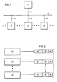
- Figure 1 is a block diagram of a general configuration for a data processing system having a plurality of central processing units (CPU's) linked to a shared memory resource via a common data bus.
- a data processing system 2 comprises at least one shared memory resource 4 coupled to a common data bus 6 via a communication line 8.
- At least one write-back cache-containing CPU 10 is coupled to the data bus 6 via a communication line 12.
- the data processing system 2 typically has a plurality of the write-back cache-containing CPU's 10.
- At least one write-through cache-containing CPU 14 is coupled to the data bus 6 via a communication line 16. Although only one of the write-through cache-containing CPU's 14 is shown in Figure 1, the system 2 typically has a plurality of the write-through cache-containing CPU's 14. At least one cache-less CPU 18 is coupled to the data bus 6 via a communication line 20. Although only one of the cache-less CPU's 18 is shown in Figure 1, the system 2 typically has a plurality of the cache-less CPU's 18.
- each block of data comprises a 32 byte data block 22.
- Each data block 22 has an associated block state field 24.
- the block state field 24 comprises a data field of 11 bits of block state information data. The first two of these bits make up a status field 26, which identifies the data block 22 as being in one of four possible states.
- the bits which are used for this purpose are shown in Table 1. Table 1 Bit 1 Bit 2 State 0 0 Free 0 1 Owned 1 0 Interlocked 1 1 Tagged Bad
- the "free” state in Table 1 indicates that the data block 22 is available to any of the CPU's 10, 14, 18 in the data processing system 2. This state occurs when the data block 22 is not accessed by any of the CPU's 10, 14, 18, regardless of the caching system it has.
- the "owned” state in Table 1 indicates that the data block 22 has been accessed by one of the write-back cache- containing CPU's 10 via a "check-out” function. This state is used to prevent the data in the data block 22 from being accessed by another one of the CPU's 10, 14, 18 until the write-back cache-containing CPU 10 that has "checked-out” the data block 22 sends a "disown" command to change the state of the data block 22 back to free.
- the "interlocked” state indicates that another one of the write-through cache-containing CPU's 14, or one of the cache-less CPU's 18, has “interlocked” the data block 22.
- the data block 22 is interlocked according to the protocol of the data processing system memory management, according to well known management methods for multiple CPU systems with write-through caches.
- This state allows CPU's to access the data block 22 via an interlock operation, rather than a "check-out” operation as used to put the data block 22 in the "owned” state.
- write-back cache-containing CPU's 10 and write-through cache-containing CPU's 14 may both operate on the same data block 22 with their own respective functions.
- the "tagged bad” state indicates that the data has been corrupted in the cache of one of the write-back cache-containing CPU's 10 with uncorrectable data error.
- the specific arrangement of bits to designate each of these states may be made other than that shown in Table 1, according to design choice.
- the bits 3 through 6 of the 11 bit block state field 24 make up a "node ID" field 28 for storing the identity of one of the CPU's 10, 14, 18 that last changed the block state of the data block 22. Whenever one of the CPU's 10, 14, 18 changes the state of the data block 22, the "node ID,” or identification, of that one of the CPU's 10, 14, 18 is written in bits 3 through 6.
- Each of the CPU's 10, 14, 18 has a node ID corresponding to a different assignment of the four bits. In this arrangement sixteen different ones of the CPU's 10, 14, 18 can be identified. If additional CPU's 10, 14, 18 are part of the data processing system 2 the number of bits in the node ID field 24 may be expanded to provide proper identification.
- the bits 7 through 11 of the 11 bit block state field 24 make up an error correction code (ECC) field 30 used for storing error correction code information.
- ECC error correction code
- These five bits are coded according to a well known modified Hamming Code to provide single bit correction and double bit detection of errors over the entire 11 bit block state field 24. If the number of bits for the ID node field 28 are expanded, the corresponding number of bits for the ECC field 30 can also be expanded as desired.
- the block state field 24 of each of the data blocks 22 changes to reflect the free, ownership, interlock or bad data status of the data blocks 22 in the shared memory resource 4 of the data processing system 2. It also changes to indicate the identity of the last one of the CPU's 10, 14, 18 to change the status field 26 in the node ID field 28, and the ECC data in the ECC field 28. The actual state of the data block is not seen by the requesting CPU's 10, 14, 18.
- the block state field 24 provides the CPU's 10, 14, 18 with data to read and write the block state directly.
- the diagnostic and control status registers of the CPU's 10, 14, 18 may be configured to allow the block state field to appear in the read data field when one of the CPU's 10, 14, 18 performs a read command to the shared memory resource 4. This is done by interchanging the 11 block state data bits from the block state field 24 with the same number of bits from the read data that is sent back to a requesting one of the CPU's 10, 14, 18. For instance, the first 11 bits of read data requested by one of the CPU's 10, 14, 18 from one of the data blocks 22 may be interchanged with the bits of its associated block state field 24. Alternately, another group of bits in the data blocks 22 may be interchanged.
- the diagnostic configuration also allows the block state field 24 to be directly written by one of the CPU's 10, 14, 18 through the use of a write command by writing in the block state field 24 with 11 bits of write data to the associated one of the data blocks 22.
- the block states may be accessed by the CPU's 10, 14, 18 for reading or rewriting even during normal operation, if necessary. For instance, the block states may need to be changed from "tagged bad” to "free".
- the bad block state indication is made by a CPU which corrupts an owned data block in its cache and writes this corrupted cached data back into memory. When this block of data is read by other CPU's, the bad block state indication, "tagged bad", informs them that the data has been corrupted.
Landscapes
- Engineering & Computer Science (AREA)
- Theoretical Computer Science (AREA)
- Physics & Mathematics (AREA)
- General Engineering & Computer Science (AREA)
- General Physics & Mathematics (AREA)
- Memory System Of A Hierarchy Structure (AREA)
- Techniques For Improving Reliability Of Storages (AREA)
- Multi Processors (AREA)
Applications Claiming Priority (2)
| Application Number | Priority Date | Filing Date | Title |
|---|---|---|---|
| US37641489A | 1989-07-06 | 1989-07-06 | |
| US376414 | 1989-07-06 |
Publications (2)
| Publication Number | Publication Date |
|---|---|
| EP0407067A2 true EP0407067A2 (fr) | 1991-01-09 |
| EP0407067A3 EP0407067A3 (en) | 1992-07-29 |
Family
ID=23484933
Family Applications (1)
| Application Number | Title | Priority Date | Filing Date |
|---|---|---|---|
| EP19900306815 Withdrawn EP0407067A3 (en) | 1989-07-06 | 1990-06-21 | Cache support architecture |
Country Status (3)
| Country | Link |
|---|---|
| EP (1) | EP0407067A3 (fr) |
| JP (1) | JPH065514B2 (fr) |
| CA (1) | CA2019727A1 (fr) |
Cited By (3)
| Publication number | Priority date | Publication date | Assignee | Title |
|---|---|---|---|---|
| EP0533373A3 (en) * | 1991-09-18 | 1993-04-21 | Ncr International Inc. | Computer system having cache memory |
| FR2683924A1 (fr) * | 1991-11-18 | 1993-05-21 | Bull Sa | Memoire integree, son procede de gestion et systeme informatique en resultant. |
| EP0600626A1 (fr) * | 1992-11-13 | 1994-06-08 | Cyrix Corporation | Cohérence d'antémémoire à postmémorisation dans un système adapté à une antémémoire à écriture en travers |
-
1990
- 1990-06-21 EP EP19900306815 patent/EP0407067A3/en not_active Withdrawn
- 1990-06-25 CA CA002019727A patent/CA2019727A1/fr not_active Abandoned
- 1990-07-05 JP JP2178499A patent/JPH065514B2/ja not_active Expired - Lifetime
Non-Patent Citations (3)
| Title |
|---|
| COMPUTER SOCIETY INTERNATIONAL CONFERENCE (COMPCON). vol. 33, 1988, IEEE,WASHINGTON D.C.,US pages 505 - 511; SWEAZEY: 'Shared memory systems on the Futurebus' * |
| HEWLETT-PACKARD JOURNAL. vol. 38, no. 9, September 1987, PALO ALTO US pages 4 - 11; MANGELSDORF ET AL.: 'A VLSI processor for HP precision architecture' * |
| IBM TECHNICAL DISCLOSURE BULLETIN. vol. 30, no. 5, October 1987, NEW YORK US pages 16 - 17; 'Locked line indication' * |
Cited By (7)
| Publication number | Priority date | Publication date | Assignee | Title |
|---|---|---|---|---|
| EP0533373A3 (en) * | 1991-09-18 | 1993-04-21 | Ncr International Inc. | Computer system having cache memory |
| FR2683924A1 (fr) * | 1991-11-18 | 1993-05-21 | Bull Sa | Memoire integree, son procede de gestion et systeme informatique en resultant. |
| EP0543712A1 (fr) * | 1991-11-18 | 1993-05-26 | Bull S.A. | Mémoire intégrée, son procédé de gestion et système informatique en résultant |
| WO1993010497A1 (fr) * | 1991-11-18 | 1993-05-27 | Bull, S.A. | Memoire integree, son procede de gestion et systeme informatique en resultant |
| US5537621A (en) * | 1991-11-18 | 1996-07-16 | Bull, S.A. | Integrated memory, method for managing it, and resultant information processing system |
| EP0600626A1 (fr) * | 1992-11-13 | 1994-06-08 | Cyrix Corporation | Cohérence d'antémémoire à postmémorisation dans un système adapté à une antémémoire à écriture en travers |
| US5524234A (en) * | 1992-11-13 | 1996-06-04 | Cyrix Corporation | Coherency for write-back cache in a system designed for write-through cache including write-back latency control |
Also Published As
| Publication number | Publication date |
|---|---|
| EP0407067A3 (en) | 1992-07-29 |
| JPH065514B2 (ja) | 1994-01-19 |
| CA2019727A1 (fr) | 1991-01-06 |
| JPH03118650A (ja) | 1991-05-21 |
Similar Documents
| Publication | Publication Date | Title |
|---|---|---|
| US7024525B2 (en) | Distributed background track processing | |
| EP1131715B1 (fr) | Systeme de traitement transactionnel reparti et procede associe | |
| US7107411B2 (en) | Apparatus method and system for fault tolerant virtual memory management | |
| US4977498A (en) | Data processing system having a data memory interlock coherency scheme | |
| US6119209A (en) | Backup directory for a write cache | |
| US5420999A (en) | Free memory cell management | |
| US7725445B2 (en) | Data replication among storage systems | |
| US5604863A (en) | Method for coordinating executing programs in a data processing system | |
| US5689678A (en) | Distributed storage array system having a plurality of modular control units | |
| US20030195886A1 (en) | Virtual storage devices | |
| KR20030084553A (ko) | 멀티프로세서 장치 | |
| JPH0526217B2 (fr) | ||
| KR100527610B1 (ko) | 저장장치,데이터처리시스템및데이터기록및판독방법 | |
| EP0407087B1 (fr) | File d'attente d'entrée de données pour un sous-système de mémoire | |
| EP0438960B1 (fr) | Antémémoire rapide à écriture au travers | |
| US20030177334A1 (en) | Address mapping for disk drive to accommodate multiple operating systems | |
| JP2746530B2 (ja) | 共有メモリマルチプロセッサ | |
| EP0407067A2 (fr) | Architecture d'assistance pour antémémoire | |
| EP0351109A2 (fr) | Réduction de ressources, dans un sous-système de stockage de données à haute fiabilité | |
| US20040059871A1 (en) | Local invalidation buses for a highly scalable shared cache memory hierarchy | |
| JPH0635802A (ja) | 複数キャッシュ付きディスク制御装置 | |
| EP0518311A2 (fr) | Procédé de stockage de fichiers, procédé d'accès de fichiers et système de traitement distribué utilisant ces procédés | |
| US6996675B2 (en) | Retrieval of all tag entries of cache locations for memory address and determining ECC based on same | |
| US6665830B2 (en) | System and method for building a checksum | |
| JPS5845120B2 (ja) | バツフア・メモリ障害制御方式 |
Legal Events
| Date | Code | Title | Description |
|---|---|---|---|
| PUAI | Public reference made under article 153(3) epc to a published international application that has entered the european phase |
Free format text: ORIGINAL CODE: 0009012 |
|
| 17P | Request for examination filed |
Effective date: 19900706 |
|
| AK | Designated contracting states |
Kind code of ref document: A2 Designated state(s): AT BE CH DE DK ES FR GB GR IT LI LU NL SE |
|
| PUAL | Search report despatched |
Free format text: ORIGINAL CODE: 0009013 |
|
| AK | Designated contracting states |
Kind code of ref document: A3 Designated state(s): AT BE CH DE DK ES FR GB GR IT LI LU NL SE |
|
| 17Q | First examination report despatched |
Effective date: 19950420 |
|
| STAA | Information on the status of an ep patent application or granted ep patent |
Free format text: STATUS: THE APPLICATION IS DEEMED TO BE WITHDRAWN |
|
| 18D | Application deemed to be withdrawn |
Effective date: 19950831 |