EP0407131A2 - Contact - Google Patents
Contact Download PDFInfo
- Publication number
- EP0407131A2 EP0407131A2 EP90307229A EP90307229A EP0407131A2 EP 0407131 A2 EP0407131 A2 EP 0407131A2 EP 90307229 A EP90307229 A EP 90307229A EP 90307229 A EP90307229 A EP 90307229A EP 0407131 A2 EP0407131 A2 EP 0407131A2
- Authority
- EP
- European Patent Office
- Prior art keywords
- contact
- nose
- pressure
- electric part
- elastically
- Prior art date
- Legal status (The legal status is an assumption and is not a legal conclusion. Google has not performed a legal analysis and makes no representation as to the accuracy of the status listed.)
- Granted
Links
Images


Classifications
-
- H—ELECTRICITY
- H05—ELECTRIC TECHNIQUES NOT OTHERWISE PROVIDED FOR
- H05K—PRINTED CIRCUITS; CASINGS OR CONSTRUCTIONAL DETAILS OF ELECTRIC APPARATUS; MANUFACTURE OF ASSEMBLAGES OF ELECTRICAL COMPONENTS
- H05K7/00—Constructional details common to different types of electric apparatus
- H05K7/02—Arrangements of circuit components or wiring on supporting structure
- H05K7/10—Plug-in assemblages of components, e.g. IC sockets
- H05K7/1015—Plug-in assemblages of components, e.g. IC sockets having exterior leads
- H05K7/1023—Plug-in assemblages of components, e.g. IC sockets having exterior leads co-operating by abutting, e.g. flat pack
Definitions
- This invention relates to a contact for connecting an electric part such as an IC package, etc. and more particularly to a contact of a socket for an electric part which is suitable for incurring an electric signal of high frequency.
- a contact disclosed in Japanese Utility Model Early Laid-open Publication No. Sho 63-117084 has such a construction as that a bypass bending element having a contact nose at one end portion thereof is displaced downwardly, the contact nose is abutted against a projecting element on the side of a male terminal disposed at the other end portion of the bypass bending portion so as to elastically displace the projecting element against its spring property, thereby to bypass the contact nose and the male terminal.
- the displacing amount of the bypass bending element is irregular.
- the displacing amount of the bypass bending portion is absorbed by elastically displacing the bypass bending element upwardly, downwardly and back wardly.
- the present invention has been accomplished in order to obviate these shortcomings.
- a contact according to the present invention includes a contact nose adapted to contact with a terminal of an electric part, and an elastic supporting element adapted to elastically support the contact nose, the nose and element being continuously formed at predetermined angles, such continuously formed portion between the nose and element being served as a pressure contact portion for contacting with a conductive member of other electric part under pressure, the elastic supporting element being displaced by serving the pressure contact portion as a supporting point and the contact nose being elastically displaced.
- the contact nose may be formed of a rigid member.
- a contact including a contact nose adapted to contact with a terminal of an electric part, and an elastic supporting element adapted to elastically support the contact nose, the nose and element being continuously formed at predetermined angles, such continuously formed portion be tween the nose and element being served as a pressure contact portion for contacting with a conductive member of other electric part under pressure, the elastic supporting element being displaced by serving the pressure contact portion as a supporting point and the contact nose being elastically displaced, the contact nose being formed of an elastically displaceable contact element and a stationary contact element embedded in a connector base and abutted against and supporting thereon the displaceable contact nose through the pressure contact portion.
- the stationary contact noses may be arranged in a zigzag form, and male terminals of adjacent stationary contact noses may be disposed in positions equal distance from the pressure contact portion.
- the contact nose When a pressure is applied to the contact nose when the electric part terminal is placed thereon, the contact nose is displaced downwardly due to elastic displacement of the elastic supporting element to provide a pressure contact with a conductive member of other electric part or a stationary contact element embedded in the connector board.
- the elastic supporting element while bending the elastic supporting element by serving the pressure contact portion as a supporting point, the circuit between the contact nose of the contact and the conductive element or between the stationary contact elements is shorted.
- the bypass object can be achieved by way of the shortest distance between the electric part mount ing contact portion and the pressure contacting portion through the contact nose, that is, by way of the shortest distance through the contact element.
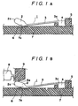
- the reference numeral 1 denotes a contact which is formed of a contact nose 2 and an elastic supporting element 2 for elastically supporting the contact nose 2.
- the contact nose and the elastic supporting element 3 are continuously formed with each other at predetermined bending angles and such bending portion 6 is served as a pressure contact portion.
- the free end of the contact nose 2 is served as a mount seat 2a for a terminal 8a of an electric part 8 such as IC, etc. to be placed thereon, and a tail end 3a of the elastic supporting element 3 is embedded in a connector base 5 through a fixed portion 4 formed on the tail end 3a.
- the contact 1 is elastically displaced by serving the bending portion 6 as a first supporting point and the tail end 3a as a second supporting point.
- the connector base 5 is fixed to a wiring board 7 and the pressure contact portion formed of the bending portion 6 formed between the contact nose 2 and the elastic supporting element 3 which form the contact 1 is abutted against and supported by a conductive member 7a of the wiring board 7.
- the conductive member 7a of the wiring board 7 and the electric part terminal are contacted with each other through the contact nose 2.
- the bypass object can be achieved by the shortest way through this contact nose 2. That is, there can be obtained a contact which exhibits a favorable characteristics with respect to a signal of high frequency.
- the bending portion 6 pressure contact portion for interconnecting the contact nose 2 and the elastic supporting element 3 is required to be placed in such a manner as to correspond to the conductive member 7a of the wiring board 7 either in its contacted state or non-contacted state. It is not necessarily be in its contacted state before it is pressurized by the pressure member 9.
- the contact 1 is not embedded in the connector base 5 and interposed between the connector base 5 and the wiring board 7.
- the tail end 3a of the elastic supporting element 3 forming the contact 1 is merely abutted against and supported by the connector base 5 in such a manner as to restrict an upward displacement, and the free end of the contact nose 2 is provided with a projecting piece 2b abutted against and supported by the connector base 5 in such a manner as to restrict the upward displacement.
- the pressure contact portion formed by the bending portion 6 is abutted against and supported by the conductive member 7a of the wiring board 7.
- the contact 1 is disposed in a three-point supported state.
- the contact 1 serves the bending portion 6 as a first supporting point, the tail end 3a as a second supporting point and the mount seat 2a as the pressurizing point.
- the contact 1 is elastically displaced by a push-down force applied to the pressurizing point at the first and second supporting points.
- FIG. 3(A) shows a connector comprising a contact 1 formed of a displaceable contact element 1A and a stationary contact element 1B.
- the displaceable contact element 1A is formed of a contact nose 2 for contacting with a terminal of an electric part and an elastic supporting element 3 for elastically supporting the contact nose 2, the nose and element 2 and 3 being continuously formed at predetermined angles, such bending portion 6 being served as a supporting point for displacing the elastic supporting element 3 so that the contact nose 2 will be elastically displaced.
- the stationary element 1B is formed of a mail terminal 10 embedded in the connector base 5 and the embedding end portion of the male terminal 10 is formed of a mounting contact element 10a for abutting against and supporting thereon the bending portion 6 of the displaceable contact element 1A.
- the free end of the elastic supporting element 3 forming the contact 1 is abutted against and supported by the connector base 5 in such a manner as to restrict an upward displacement, and the free end of the contact nose 2 is provided with a projecting piece 2b which is abutted against and supported by the connector base 5 in such a manner as to restrict the upward displacement. Furthermore, the pressure contact member formed by the bending portion 6 is abutted against and supported by the stationary contact element 1B. In this way, the contact 1 is supported at three points.
- This embodiment shows another example, in which the mounting contact element 10a of the stationary contact element 1B of the third embodiment is formed of an elastic piece which is elastically displaced in the pressure applying direction.
- the displaceable contact element 1A can be embedded in the connector base 5 through the stationary portion 4 as in the first embodiment.
- the contact nose 2 of the first through fourth embodiments is formed of a rigid member in order to obtain displacement of the contact nose 2 which is required in order to obtain a pressure contact by the elastic supporting element 3.
- the connector is formed in the manner as in the third and fourth embodiment and the stationary contact elements 1B are arranged in a zigzag form, the male terminals 10 of the adjacent stationary terminals being disposed in positions equal distance from the bending portion 6. In this way, a high density embedding can be obtained.
- a contact of a simple structure which is capable of achieving the bypass object through the shortest distance while obtaining a favorable elasticity which is required to the mounting contact of the electric part terminal.
- the contact nose forming the contact provides a favorable pressure contact while bending the elastic supporting element by serving the bending portion (pressure contact portion) by the elastic function of the elastic supporting element, and at the same time, is capable of effectively achieve the bypass object through the shortest distance by way of the contact nose.
- the contact of the present invention can be greatly reduced in bulk when compared with the conventional contact having the U-shaped bypass element, thus enabling to miniaturize the contact.
Landscapes
- Engineering & Computer Science (AREA)
- Microelectronics & Electronic Packaging (AREA)
- Coupling Device And Connection With Printed Circuit (AREA)
- Testing Of Individual Semiconductor Devices (AREA)
- Connecting Device With Holders (AREA)
Applications Claiming Priority (2)
| Application Number | Priority Date | Filing Date | Title |
|---|---|---|---|
| JP172691/89 | 1989-07-04 | ||
| JP1172691A JP2554746B2 (ja) | 1989-07-04 | 1989-07-04 | コンタクト |
Publications (3)
| Publication Number | Publication Date |
|---|---|
| EP0407131A2 true EP0407131A2 (fr) | 1991-01-09 |
| EP0407131A3 EP0407131A3 (en) | 1991-08-28 |
| EP0407131B1 EP0407131B1 (fr) | 1994-10-05 |
Family
ID=15946568
Family Applications (1)
| Application Number | Title | Priority Date | Filing Date |
|---|---|---|---|
| EP90307229A Expired - Lifetime EP0407131B1 (fr) | 1989-07-04 | 1990-07-02 | Contact |
Country Status (6)
| Country | Link |
|---|---|
| US (1) | US5035629A (fr) |
| EP (1) | EP0407131B1 (fr) |
| JP (1) | JP2554746B2 (fr) |
| CA (1) | CA2020152A1 (fr) |
| DE (1) | DE69013082T2 (fr) |
| MY (1) | MY107121A (fr) |
Cited By (2)
| Publication number | Priority date | Publication date | Assignee | Title |
|---|---|---|---|---|
| EP0503809A3 (en) * | 1991-03-15 | 1993-02-24 | Yamaichi Electric Co., Ltd. | Mount-to-contact type contact |
| EP0919816B1 (fr) * | 1997-11-25 | 2006-12-27 | Kabushiki Kaisha Nihon Micronics | Dispositif de connexion électrique |
Families Citing this family (21)
| Publication number | Priority date | Publication date | Assignee | Title |
|---|---|---|---|---|
| JP3187904B2 (ja) * | 1991-12-20 | 2001-07-16 | 山一電機株式会社 | 電気部品用接続器 |
| US5626481A (en) * | 1995-06-12 | 1997-05-06 | Yamaichi Electronics Co., Ltd. | Structure for electrical connection of electric part |
| MY115876A (en) * | 1995-11-17 | 2003-09-30 | Tesec Kk | Electronic component connector |
| JP2746869B2 (ja) * | 1996-07-05 | 1998-05-06 | 株式会社エンプラス | Icソケット |
| US5746626A (en) * | 1996-10-11 | 1998-05-05 | Bourns, Inc. | Electrical connector assembly |
| JP3379897B2 (ja) * | 1997-02-10 | 2003-02-24 | 株式会社日本マイクロニクス | 被検査体試験用補助装置 |
| JPH1126125A (ja) * | 1997-07-01 | 1999-01-29 | Japan Aviation Electron Ind Ltd | Icソケット |
| JP3577416B2 (ja) * | 1997-11-25 | 2004-10-13 | 株式会社日本マイクロニクス | 電気的接続装置 |
| JP3810977B2 (ja) * | 2000-02-25 | 2006-08-16 | 株式会社エンプラス | 電気部品用ソケット |
| US6672912B2 (en) * | 2000-03-31 | 2004-01-06 | Intel Corporation | Discrete device socket and method of fabrication therefor |
| AU2002236552A1 (en) * | 2000-11-20 | 2002-05-27 | Intel Corporation | High performance heat sink configurations for use in high density packaging applications |
| US6633484B1 (en) | 2000-11-20 | 2003-10-14 | Intel Corporation | Heat-dissipating devices, systems, and methods with small footprint |
| US6501655B1 (en) | 2000-11-20 | 2002-12-31 | Intel Corporation | High performance fin configuration for air cooled heat sinks |
| US6388207B1 (en) | 2000-12-29 | 2002-05-14 | Intel Corporation | Electronic assembly with trench structures and methods of manufacture |
| US6671172B2 (en) * | 2001-09-10 | 2003-12-30 | Intel Corporation | Electronic assemblies with high capacity curved fin heat sinks |
| JP4053786B2 (ja) * | 2002-02-27 | 2008-02-27 | 株式会社エンプラス | 電気部品用ソケット |
| JP4117827B2 (ja) * | 2002-08-09 | 2008-07-16 | 株式会社エンプラス | 電気部品用ソケット |
| JP4279039B2 (ja) * | 2003-04-22 | 2009-06-17 | 株式会社エンプラス | 電気部品用ソケット |
| JP4303045B2 (ja) * | 2003-06-25 | 2009-07-29 | 株式会社エンプラス | 電気部品用キャリア |
| US9261536B2 (en) * | 2012-08-14 | 2016-02-16 | Asm Technology Singapore Pte Ltd | Test contactor for electrical testing of electronic components |
| US10908182B2 (en) * | 2016-06-28 | 2021-02-02 | Kabushiki Kaisha Nihon Micronics | Electrical connecting apparatus and contact |
Family Cites Families (13)
| Publication number | Priority date | Publication date | Assignee | Title |
|---|---|---|---|---|
| US3470522A (en) * | 1968-02-26 | 1969-09-30 | Bunker Ramo | Electrical connector |
| GB1281535A (en) * | 1968-12-13 | 1972-07-12 | Bicc Burndy Ltd | An improved electrical connector |
| US4027935A (en) * | 1976-06-21 | 1977-06-07 | International Business Machines Corporation | Contact for an electrical contactor assembly |
| US4176895A (en) * | 1978-09-27 | 1979-12-04 | Burroughs Corporation | High density double contacting connector assembly for leadless integrated circuit packages |
| AU7046981A (en) * | 1980-05-27 | 1982-01-21 | Amp Incorporated | Electrical contact receptacle |
| US4362353A (en) * | 1980-05-27 | 1982-12-07 | Amp Incorporated | Contact clip for connecting a ceramic substrate to a printed circuit board |
| US4494807A (en) * | 1982-12-27 | 1985-01-22 | Amp Incorporated | Low profile chip carrier contact |
| US4547028A (en) * | 1983-10-05 | 1985-10-15 | A P Products Incorporated | Low profile test clip |
| US4583806A (en) * | 1985-01-11 | 1986-04-22 | Bourns, Inc. | Low insertion-force socket for IC device |
| US4684184A (en) * | 1986-01-14 | 1987-08-04 | Amp Incorporated | Chip carrier and carrier socket for closely spaced contacts |
| JPS63117084A (ja) * | 1986-10-31 | 1988-05-21 | Pilot Ink Co Ltd | ボ−ルペン用水性インク組成物 |
| JPS63164191A (ja) * | 1986-12-25 | 1988-07-07 | 松下電器産業株式会社 | 電気ホツトプレ−トの制御装置 |
| US4941832A (en) * | 1989-01-30 | 1990-07-17 | Amp Incorporated | Low profile chip carrier socket |
-
1989
- 1989-07-04 JP JP1172691A patent/JP2554746B2/ja not_active Expired - Fee Related
-
1990
- 1990-06-29 MY MYPI90001110A patent/MY107121A/en unknown
- 1990-06-29 CA CA002020152A patent/CA2020152A1/fr not_active Abandoned
- 1990-07-02 DE DE69013082T patent/DE69013082T2/de not_active Expired - Fee Related
- 1990-07-02 EP EP90307229A patent/EP0407131B1/fr not_active Expired - Lifetime
- 1990-07-03 US US07/547,999 patent/US5035629A/en not_active Expired - Lifetime
Cited By (2)
| Publication number | Priority date | Publication date | Assignee | Title |
|---|---|---|---|---|
| EP0503809A3 (en) * | 1991-03-15 | 1993-02-24 | Yamaichi Electric Co., Ltd. | Mount-to-contact type contact |
| EP0919816B1 (fr) * | 1997-11-25 | 2006-12-27 | Kabushiki Kaisha Nihon Micronics | Dispositif de connexion électrique |
Also Published As
| Publication number | Publication date |
|---|---|
| JPH0337983A (ja) | 1991-02-19 |
| EP0407131A3 (en) | 1991-08-28 |
| DE69013082T2 (de) | 1995-05-18 |
| US5035629A (en) | 1991-07-30 |
| CA2020152A1 (fr) | 1991-01-05 |
| MY107121A (en) | 1995-09-30 |
| EP0407131B1 (fr) | 1994-10-05 |
| DE69013082D1 (de) | 1994-11-10 |
| JP2554746B2 (ja) | 1996-11-13 |
Similar Documents
| Publication | Publication Date | Title |
|---|---|---|
| EP0407131A2 (fr) | Contact | |
| US4645279A (en) | Chip carrier socket having improved contact terminals | |
| US4975068A (en) | Flexible cable connector | |
| EP1583406A3 (fr) | Ensemble d'interconnexion pour panneaux à circuit imprimé | |
| EP0166526A2 (fr) | Socle et contacts pour le logement des circuits intégrés | |
| US4941832A (en) | Low profile chip carrier socket | |
| CN1125538C (zh) | 安装于壳体内用于便携式无线电装置的内置天线 | |
| US6508675B1 (en) | Electrical connector configured by wafers including moveable contacts | |
| EP0817317A3 (fr) | Structure de connexion de câbles avec un élément de détection | |
| EP0923161A3 (fr) | Connecteur électrique pour circuits plats | |
| EP0549161A1 (fr) | Connecteur pour composants électriques | |
| US6224388B1 (en) | In-board connector | |
| JP2004172128A (ja) | 2重コンタクト電気的圧縮コネクタ | |
| US5161982A (en) | Reactive base for cantilevered connector | |
| JPH08125360A (ja) | パッケージへの給電装置 | |
| JPH04133365U (ja) | エラストマーコネクタ | |
| JPH09129288A (ja) | 表面実装型コネクタ及びその製造方法 | |
| JP2004296419A (ja) | コネクタ | |
| EP0795932A2 (fr) | Connecteur | |
| US5669784A (en) | Surface mount type IC socket | |
| JP4098071B2 (ja) | コンタクト | |
| WO2003052876A2 (fr) | Procede et dispositif de connexion de cartes de circuits imprimees pour un ensemble de detection | |
| JP3536196B2 (ja) | ソケット | |
| JP3337337B2 (ja) | コネクタの組立方法 | |
| JP2003257520A (ja) | 押し当て式基板用コネクター |
Legal Events
| Date | Code | Title | Description |
|---|---|---|---|
| PUAI | Public reference made under article 153(3) epc to a published international application that has entered the european phase |
Free format text: ORIGINAL CODE: 0009012 |
|
| AK | Designated contracting states |
Kind code of ref document: A2 Designated state(s): DE FR GB IT |
|
| PUAL | Search report despatched |
Free format text: ORIGINAL CODE: 0009013 |
|
| AK | Designated contracting states |
Kind code of ref document: A3 Designated state(s): DE FR GB IT |
|
| 17P | Request for examination filed |
Effective date: 19911114 |
|
| 17Q | First examination report despatched |
Effective date: 19930318 |
|
| GRAA | (expected) grant |
Free format text: ORIGINAL CODE: 0009210 |
|
| RAP1 | Party data changed (applicant data changed or rights of an application transferred) |
Owner name: YAMAICHI ELECTRONICS CO., LTD. |
|
| AK | Designated contracting states |
Kind code of ref document: B1 Designated state(s): DE FR GB IT |
|
| ET | Fr: translation filed | ||
| REF | Corresponds to: |
Ref document number: 69013082 Country of ref document: DE Date of ref document: 19941110 |
|
| ITF | It: translation for a ep patent filed | ||
| RAP4 | Party data changed (patent owner data changed or rights of a patent transferred) |
Owner name: YAMAICHI ELECTRONICS CO., LTD. |
|
| PLBE | No opposition filed within time limit |
Free format text: ORIGINAL CODE: 0009261 |
|
| STAA | Information on the status of an ep patent application or granted ep patent |
Free format text: STATUS: NO OPPOSITION FILED WITHIN TIME LIMIT |
|
| 26N | No opposition filed | ||
| PG25 | Lapsed in a contracting state [announced via postgrant information from national office to epo] |
Ref country code: DE Effective date: 19960402 |
|
| PG25 | Lapsed in a contracting state [announced via postgrant information from national office to epo] |
Ref country code: FR Effective date: 19960430 |
|
| REG | Reference to a national code |
Ref country code: FR Ref legal event code: ST |
|
| REG | Reference to a national code |
Ref country code: FR Ref legal event code: ST |
|
| REG | Reference to a national code |
Ref country code: FR Ref legal event code: ST |
|
| PGFP | Annual fee paid to national office [announced via postgrant information from national office to epo] |
Ref country code: GB Payment date: 19960626 Year of fee payment: 7 |
|
| PG25 | Lapsed in a contracting state [announced via postgrant information from national office to epo] |
Ref country code: GB Free format text: LAPSE BECAUSE OF NON-PAYMENT OF DUE FEES Effective date: 19970702 |
|
| GBPC | Gb: european patent ceased through non-payment of renewal fee |
Effective date: 19970702 |
|
| PG25 | Lapsed in a contracting state [announced via postgrant information from national office to epo] |
Ref country code: IT Free format text: LAPSE BECAUSE OF NON-PAYMENT OF DUE FEES Effective date: 20050702 |