EP0408231A1 - Panneau plat électroluminescent à film mince intégré et structure émettant sur la tranche produisant des sources de lumière multiples - Google Patents
Panneau plat électroluminescent à film mince intégré et structure émettant sur la tranche produisant des sources de lumière multiples Download PDFInfo
- Publication number
- EP0408231A1 EP0408231A1 EP90307225A EP90307225A EP0408231A1 EP 0408231 A1 EP0408231 A1 EP 0408231A1 EP 90307225 A EP90307225 A EP 90307225A EP 90307225 A EP90307225 A EP 90307225A EP 0408231 A1 EP0408231 A1 EP 0408231A1
- Authority
- EP
- European Patent Office
- Prior art keywords
- flat panel
- panel structure
- face
- emitter portion
- edge emitter
- Prior art date
- Legal status (The legal status is an assumption and is not a legal conclusion. Google has not performed a legal analysis and makes no representation as to the accuracy of the status listed.)
- Granted
Links
Images
Classifications
-
- H—ELECTRICITY
- H05—ELECTRIC TECHNIQUES NOT OTHERWISE PROVIDED FOR
- H05B—ELECTRIC HEATING; ELECTRIC LIGHT SOURCES NOT OTHERWISE PROVIDED FOR; CIRCUIT ARRANGEMENTS FOR ELECTRIC LIGHT SOURCES, IN GENERAL
- H05B33/00—Electroluminescent light sources
- H05B33/12—Light sources with substantially two-dimensional [2D] radiating surfaces
Definitions
- the present invention relates generally to a thin film electroluminescent multiple light source, and more particularly, is concerned with an integrated TFEL flat panel face and edge emitter structure for simultaneously functioning as multiple light sources.
- Electroluminescence is a phenomena which occurs in certain materials from the passage of an electric current through the material.
- the electric current excites the electrons of the dopant in the light emitting material to higher energy levels.
- Emission of radiation thereafter occurs as the electrons emit or give up the excitation energy and fall back to lower energy levels.
- Such electrons can only have certain discrete energies. Therefore, the excitation energy is emitted or radiated at specific wavelengths depending on the particular material.
- TFEL Thin film electroluminescent
- TFEL Thin film electroluminescent
- One arrangement which utilizes the TFEL device to provide the light source is a flat panel display system, such as disclosed in US-A 4,110,664 and US-A 4,006,383.
- a TFEL flat panel display system light emissions are produced substantially normal to a face of the device and so provide the light source at the device face.
- Another arrangement utilizing the TFEL device to provide the light source is a line array, or edge, emitter, such as disclosed in US-A 4,535,341.
- TFEL edge emitter system In a TFEL edge emitter system, light emissions are produced substantially normal to an edge of the device and so provide the light source at the device edge.
- a printer is disclosed in US-A 4,535,341 which employs a TFEL edge emitter device as the light source.
- the TFEL device either as a face emitter structure for applications requiring a large area light source, such as a flat panel display, or as an edge emitter structure for applications requiring only a narrow light source, such as a light-activated printer.
- a face emitter structure for applications requiring a large area light source, such as a flat panel display
- an edge emitter structure for applications requiring only a narrow light source, such as a light-activated printer.
- unknown in the prior art is an integrated structure which provides the TFEL device as both face and edge emitter devices suitable for applications which heretofore have been assumed to require separate components.
- the present invention provides an integrated TFEL flat panel face and edge emitter structure designed to fill the gap left by the prior art.
- the integrated TFEL flat panel structure can produce multiple light sources for concurrent applications, such as displaying and printing the same image.
- the invention consists in a thin film electroluminescent (TFEL) multiple light source device, comprising a thin film electroluminescent flat panel structure having front and rear faces and side edges extending between said faces, said panel structure being composed of a face emitter portion and an edge emitter portion, said face emitter portion being operable for emitting light energy from one of said front and back faces of said flat panel structure in a direction substantially perpendicular to the plane of said flat panel structure, said edge emitter portion being operable for emitting light energy from one of said side edges of said flat panel structure in a direction substantially parallel to the plane of said flat panel structure.
- TFEL thin film electroluminescent
- each portion preferably share a common substrate.
- each portion includes a pair of electrode layers, at least one and preferably a pair of dielectric layers interposed between the electrode layers and a layer of light generating material, such as phosphor, interposed between the dielectric layers.
- the electrode layers, dielectric layers and phosphor layer are formed in a generally stacked laminar arrangement and are disposed on the common layer of substrate material.
- TFEL flat panel face and edge emitter structure which can provide a solid state, electronically controlled high resolution multiple light source.
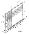
- the integrated emitter structure is a TFEL flat panel 10 having front and rear faces 12, 14 and side edges 16, 18, 20, 22 extending between the faces 12, 14.
- TFEL flat panel 10 is composed of a face emitter portion 10A and an edge emitter portion 10B.
- the face emitter portion 10A is operable for emitting light energy from one of the faces, for example the front face 12, of the flat panel 10 in the direction of arrow A which is substantially perpendicular to the plane of the flat panel 10.
- the edge emitter portion 10B is operable for emitting light energy from one of the side edges, for example the bottom edge 16, of the flat panel 10 in the direction of arrow B which is substantially perpendicular to arrow A and parallel to the plane of the flat panel 10.
- the face and edge emitter portions 10A, 10B of the flat panel 10 can share a common substrate 24, as shown in Fig. 1, or separate substrates placed end-to-end, as represented by the dashed line in Fig. 1.
- the material of the substrate 24 is typically glass which is transparent to light energy.
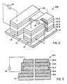
- the face and edge emitter portions 10A, 10B of the flat panel 10 each employ a laminar stack of substantially identical layers.
- the respective face and edge emitter portions 10A, 10B are each composed of a pair of electrode layers 26A, 28A and 26B, 28B, at least one and preferably a pair of dielectric layers 30A, 32A and 30B, 32B interposed between the electrode layers and an active layer 34A, 34B of light generating material interposed between the dielectric layers.
- the dielectric layers 30A, 32A and 30B, 32B are composed of a high dielectric strength, high dielectric constant material, preferably yttrium oxide (Y2O3).
- the layer 34A, 34B of light generating material is preferably zinc sulfide doped with manganese (ZnS:Mn).
- the control electrodes 28A, 28B of the face and edge emitter portions 10A, 10B are separate from one another permitting selective excitation for creating images in the light emitted by the layers 34A, 34B. The same or different images can be created.
- An electrical connector 35 is shown in Fig. 1 connected to the control electrodes 28B of the edge emitter portion 10B.
- the control electrodes 28A of the face emitter portion 10A are shown in the form of a matrix in Fig. 1.
- the layers 26A, 28A, 30A, 32A of the face emitter portion 10B can be integral with the layers 26B, 28B, 30B, 32B of the edge emitter portion 10B of the flat panel 10.
- the respective stacks of layers of the face and edge emitter portions 10A, 10B can be optically separated or isolated from one another to avoid cross talk and noise between them.
- the separated stacks can still be disposed on a common layer 24 of substrate material.
- an alternating current source 36, 38 coupled across the electrode layers 26A, 28A and 26B, 28B is operated to energize the respective face and edge emitter portions 10A, 10B.
- the active layer 34A, 34B will luminesce and light emitted therefrom will be externally transmitted through the front face 12 and bottom edge 16, respectively.
- the light transmits through the front face 12 of the face emitter portion 10A of the flat panel 10 in view that the electrode layer 28A at the back face 14 is opaque or non-transparent to light energy, whereas the electrode layer 26A at the front face 12 next to the substrate 24 is transparent to light energy.
- all side edges 18, 20, 22 of the flat panel 10, except the bottom side edge 16 of the edge emitter portion 10B are opaque to light energy.
- the light transmits through the bottom edge 16 of the edge emitter portion 10B of the flat panel 10 in view that both electrode layers 26B, 28B are opaque or non-transparent to light energy.
- the transparent electrode can be composed of indium-tin oxide (In,Sn)O2
- the opaque electrodes can be composed of aluminum (Al).
- the edge emitter portion 10B can be provided as a multiplicity of pixels 40 separated by a generally rectangular channel 42 formed in the TFEL flat panel bottom edge 16.
- the channel 42 typically extends vertically through the layers 26, 28, 30, 32 to the substrate 24 and also a preselected distance rearwardly from the edge 16 into the central portion of the TFEL edge emitter portion 10B.
- the channels 42 serve to optically isolate adjacent pixels from one another to prevent optical cross-talk.
- the front edges of the pixels 40 of the TFEL edge emitter portion 10B are the light emission sources thereof.
- the rear edges (not shown) of the pixels 40 are coated with a layer of non-metallic reflective coating.
- Potential applications for the integrated TFEL flat panel face and edge emitter structure are those where concurrent light images are desired, for example, a display provided by the face emitter portion 10A for generating a visual picture and a printhead provided by the edge emitter portion 10B for generating a hard copy.
Landscapes
- Electroluminescent Light Sources (AREA)
- Devices For Indicating Variable Information By Combining Individual Elements (AREA)
Applications Claiming Priority (2)
| Application Number | Priority Date | Filing Date | Title |
|---|---|---|---|
| US07/377,690 US5101137A (en) | 1989-07-10 | 1989-07-10 | Integrated tfel flat panel face and edge emitter structure producing multiple light sources |
| US377690 | 1989-07-10 |
Publications (2)
| Publication Number | Publication Date |
|---|---|
| EP0408231A1 true EP0408231A1 (fr) | 1991-01-16 |
| EP0408231B1 EP0408231B1 (fr) | 1994-05-18 |
Family
ID=23490142
Family Applications (1)
| Application Number | Title | Priority Date | Filing Date |
|---|---|---|---|
| EP90307225A Expired - Lifetime EP0408231B1 (fr) | 1989-07-10 | 1990-07-02 | Panneau plat électroluminescent à film mince intégré et structure émettant sur la tranche produisant des sources de lumière multiples |
Country Status (5)
| Country | Link |
|---|---|
| US (1) | US5101137A (fr) |
| EP (1) | EP0408231B1 (fr) |
| JP (1) | JPH0353493A (fr) |
| CA (1) | CA2017709A1 (fr) |
| DE (1) | DE69008947T2 (fr) |
Cited By (3)
| Publication number | Priority date | Publication date | Assignee | Title |
|---|---|---|---|---|
| EP0452142A3 (en) * | 1990-04-13 | 1992-03-18 | Westinghouse Electric Corporation | Light emitting edge structure with uniform light emission filter |
| EP0758177A3 (fr) * | 1990-05-22 | 1998-06-10 | Westinghouse Electric Corporation | Dispositif de facsimilé utilisant un dispositif électroluminescent en couches minces |
| EP0748145A3 (fr) * | 1995-06-07 | 1998-10-14 | Hewlett-Packard Company | Dispositif électroluminescent comme source de scanner |
Families Citing this family (11)
| Publication number | Priority date | Publication date | Assignee | Title |
|---|---|---|---|---|
| US5536193A (en) | 1991-11-07 | 1996-07-16 | Microelectronics And Computer Technology Corporation | Method of making wide band gap field emitter |
| US5449970A (en) | 1992-03-16 | 1995-09-12 | Microelectronics And Computer Technology Corporation | Diode structure flat panel display |
| US5686791A (en) | 1992-03-16 | 1997-11-11 | Microelectronics And Computer Technology Corp. | Amorphic diamond film flat field emission cathode |
| US6127773A (en) | 1992-03-16 | 2000-10-03 | Si Diamond Technology, Inc. | Amorphic diamond film flat field emission cathode |
| US5675216A (en) | 1992-03-16 | 1997-10-07 | Microelectronics And Computer Technololgy Corp. | Amorphic diamond film flat field emission cathode |
| US5543684A (en) | 1992-03-16 | 1996-08-06 | Microelectronics And Computer Technology Corporation | Flat panel display based on diamond thin films |
| JP3726117B2 (ja) | 1993-11-04 | 2005-12-14 | ナノ・プラプライアテリ、インク | 平坦パネル・ディスプレイ・システムと構成部品とを製造する方法 |
| US5445550A (en) * | 1993-12-22 | 1995-08-29 | Xie; Chenggang | Lateral field emitter device and method of manufacturing same |
| JP4365940B2 (ja) * | 1999-07-02 | 2009-11-18 | セイコーエプソン株式会社 | デジタルプリンタ |
| KR20020031202A (ko) * | 2000-10-23 | 2002-05-01 | 구본준, 론 위라하디락사 | 투명도가 낮은 기판을 이용한 평판 표시 장치 |
| KR100799591B1 (ko) * | 2006-12-07 | 2008-01-30 | 한국전자통신연구원 | 금속-절연체 전이층을 포함하는 전계발광소자 |
Citations (4)
| Publication number | Priority date | Publication date | Assignee | Title |
|---|---|---|---|---|
| US4535341A (en) * | 1983-08-19 | 1985-08-13 | Westinghouse Electric Corp. | Thin film electroluminescent line array emitter and printer |
| US4899184A (en) * | 1989-04-24 | 1990-02-06 | Westinghouse Electric Corp. | Multiplexed thin film electroluminescent edge emitter structure and electronic drive system therefrom |
| EP0369755A2 (fr) * | 1988-11-18 | 1990-05-23 | Westinghouse Electric Corporation | Structure électroluminescente émettrice de lumière latérale à film mince sur un substrat au silicium |
| EP0372942A2 (fr) * | 1988-12-07 | 1990-06-13 | Westinghouse Electric Corporation | Structure électroluminescente à film mince émettant sur la tranche |
Family Cites Families (5)
| Publication number | Priority date | Publication date | Assignee | Title |
|---|---|---|---|---|
| US4006383A (en) * | 1975-11-28 | 1977-02-01 | Westinghouse Electric Corporation | Electroluminescent display panel with enlarged active display areas |
| US4110664A (en) * | 1977-04-15 | 1978-08-29 | Westinghouse Electric Corp. | Electroluminescent bargraph with integral thin-film transistor control circuitry |
| US4464602A (en) * | 1982-01-28 | 1984-08-07 | The United States Of America As Represented By The Secretary Of The Army | Thin film electroluminescent device |
| JPS61286866A (ja) * | 1985-06-14 | 1986-12-17 | Nec Home Electronics Ltd | 光プリンタ |
| JPS6391998A (ja) * | 1986-10-03 | 1988-04-22 | オリンパス光学工業株式会社 | El発光アレイ |
-
1989
- 1989-07-10 US US07/377,690 patent/US5101137A/en not_active Expired - Fee Related
-
1990
- 1990-05-28 CA CA002017709A patent/CA2017709A1/fr not_active Abandoned
- 1990-07-02 EP EP90307225A patent/EP0408231B1/fr not_active Expired - Lifetime
- 1990-07-02 DE DE69008947T patent/DE69008947T2/de not_active Expired - Fee Related
- 1990-07-09 JP JP2181380A patent/JPH0353493A/ja active Pending
Patent Citations (4)
| Publication number | Priority date | Publication date | Assignee | Title |
|---|---|---|---|---|
| US4535341A (en) * | 1983-08-19 | 1985-08-13 | Westinghouse Electric Corp. | Thin film electroluminescent line array emitter and printer |
| EP0369755A2 (fr) * | 1988-11-18 | 1990-05-23 | Westinghouse Electric Corporation | Structure électroluminescente émettrice de lumière latérale à film mince sur un substrat au silicium |
| EP0372942A2 (fr) * | 1988-12-07 | 1990-06-13 | Westinghouse Electric Corporation | Structure électroluminescente à film mince émettant sur la tranche |
| US4899184A (en) * | 1989-04-24 | 1990-02-06 | Westinghouse Electric Corp. | Multiplexed thin film electroluminescent edge emitter structure and electronic drive system therefrom |
Cited By (4)
| Publication number | Priority date | Publication date | Assignee | Title |
|---|---|---|---|---|
| EP0452142A3 (en) * | 1990-04-13 | 1992-03-18 | Westinghouse Electric Corporation | Light emitting edge structure with uniform light emission filter |
| EP0758177A3 (fr) * | 1990-05-22 | 1998-06-10 | Westinghouse Electric Corporation | Dispositif de facsimilé utilisant un dispositif électroluminescent en couches minces |
| EP0748145A3 (fr) * | 1995-06-07 | 1998-10-14 | Hewlett-Packard Company | Dispositif électroluminescent comme source de scanner |
| KR100439390B1 (ko) * | 1995-06-07 | 2004-08-04 | 휴렛-팩커드 컴퍼니(델라웨어주법인) | 전자발광장치 |
Also Published As
| Publication number | Publication date |
|---|---|
| DE69008947D1 (de) | 1994-06-23 |
| DE69008947T2 (de) | 1995-01-05 |
| EP0408231B1 (fr) | 1994-05-18 |
| CA2017709A1 (fr) | 1991-01-10 |
| JPH0353493A (ja) | 1991-03-07 |
| US5101137A (en) | 1992-03-31 |
Similar Documents
| Publication | Publication Date | Title |
|---|---|---|
| EP0408231B1 (fr) | Panneau plat électroluminescent à film mince intégré et structure émettant sur la tranche produisant des sources de lumière multiples | |
| US4535341A (en) | Thin film electroluminescent line array emitter and printer | |
| EP0598764B1 (fr) | Affichage fluorescent electronique ameliore | |
| GB2254486A (en) | Flat image-display apparatus. | |
| JPH0973983A (ja) | El発光装置 | |
| JPS6040617B2 (ja) | メモリ性デイスプレイ | |
| US4977350A (en) | Color electroluminescence display panel having alternately-extending electrode groups | |
| JP2914981B2 (ja) | 表示装置 | |
| JPH08203669A (ja) | El両面発光表示体 | |
| US4894116A (en) | Phosphor only etching process for TFEL panel having multiple-colored display | |
| US5489817A (en) | Electron-optical terminal image device based on a cold cathode | |
| WO2021053273A1 (fr) | Dispositif électroluminescent à film mince transparent | |
| KR100248949B1 (ko) | 전계방출형 디바이스 | |
| EP0369755B1 (fr) | Structure électroluminescente émettrice de lumière latérale à film mince sur un substrat au silicium | |
| US6621231B1 (en) | Structure of a barrier in a plasma display panel | |
| US5252895A (en) | TFEL edge emitter structure with light emitting face at angle greater than ninety degrees to substrate street | |
| US5043632A (en) | TFEL edge emitter structure with uniform light emission filter | |
| WO1988009268A1 (fr) | Procede de fabrication de panneaux en couleurs d'electrodes a couche mince | |
| US7397181B2 (en) | Image display panel consisting of a matrix of memory-effect electroluminescent cells | |
| KR20060126460A (ko) | 전계발광 시스템 | |
| JPS63121296A (ja) | 薄膜発光素子 | |
| KR100719557B1 (ko) | 전극 단자부 구조 및 이를 구비한 플라즈마 디스플레이패널 | |
| JP2929999B2 (ja) | 蛍光プリントヘッド | |
| JPS6212623B2 (fr) | ||
| KR940007961B1 (ko) | 광 어드레스 방식의 전계 발광 화상 표시 장치 |
Legal Events
| Date | Code | Title | Description |
|---|---|---|---|
| PUAI | Public reference made under article 153(3) epc to a published international application that has entered the european phase |
Free format text: ORIGINAL CODE: 0009012 |
|
| AK | Designated contracting states |
Kind code of ref document: A1 Designated state(s): DE FR GB IT |
|
| 17P | Request for examination filed |
Effective date: 19910712 |
|
| 17Q | First examination report despatched |
Effective date: 19930830 |
|
| GRAA | (expected) grant |
Free format text: ORIGINAL CODE: 0009210 |
|
| AK | Designated contracting states |
Kind code of ref document: B1 Designated state(s): DE FR GB IT |
|
| REF | Corresponds to: |
Ref document number: 69008947 Country of ref document: DE Date of ref document: 19940623 |
|
| ET | Fr: translation filed | ||
| ITF | It: translation for a ep patent filed | ||
| PLBE | No opposition filed within time limit |
Free format text: ORIGINAL CODE: 0009261 |
|
| STAA | Information on the status of an ep patent application or granted ep patent |
Free format text: STATUS: NO OPPOSITION FILED WITHIN TIME LIMIT |
|
| 26N | No opposition filed | ||
| PGFP | Annual fee paid to national office [announced via postgrant information from national office to epo] |
Ref country code: GB Payment date: 19970620 Year of fee payment: 8 |
|
| PGFP | Annual fee paid to national office [announced via postgrant information from national office to epo] |
Ref country code: FR Payment date: 19970711 Year of fee payment: 8 |
|
| PGFP | Annual fee paid to national office [announced via postgrant information from national office to epo] |
Ref country code: DE Payment date: 19970729 Year of fee payment: 8 |
|
| PG25 | Lapsed in a contracting state [announced via postgrant information from national office to epo] |
Ref country code: GB Free format text: LAPSE BECAUSE OF NON-PAYMENT OF DUE FEES Effective date: 19980702 |
|
| GBPC | Gb: european patent ceased through non-payment of renewal fee |
Effective date: 19980702 |
|
| PG25 | Lapsed in a contracting state [announced via postgrant information from national office to epo] |
Ref country code: FR Free format text: LAPSE BECAUSE OF NON-PAYMENT OF DUE FEES Effective date: 19990331 |
|
| PG25 | Lapsed in a contracting state [announced via postgrant information from national office to epo] |
Ref country code: DE Free format text: LAPSE BECAUSE OF NON-PAYMENT OF DUE FEES Effective date: 19990501 |
|
| REG | Reference to a national code |
Ref country code: FR Ref legal event code: ST |
|
| PG25 | Lapsed in a contracting state [announced via postgrant information from national office to epo] |
Ref country code: IT Free format text: LAPSE BECAUSE OF NON-PAYMENT OF DUE FEES;WARNING: LAPSES OF ITALIAN PATENTS WITH EFFECTIVE DATE BEFORE 2007 MAY HAVE OCCURRED AT ANY TIME BEFORE 2007. THE CORRECT EFFECTIVE DATE MAY BE DIFFERENT FROM THE ONE RECORDED. Effective date: 20050702 |