EP0411529A1 - Synchroner digitaler Sender - Google Patents
Synchroner digitaler Sender Download PDFInfo
- Publication number
- EP0411529A1 EP0411529A1 EP90114571A EP90114571A EP0411529A1 EP 0411529 A1 EP0411529 A1 EP 0411529A1 EP 90114571 A EP90114571 A EP 90114571A EP 90114571 A EP90114571 A EP 90114571A EP 0411529 A1 EP0411529 A1 EP 0411529A1
- Authority
- EP
- European Patent Office
- Prior art keywords
- interruptions
- serial
- clock
- timer
- processing
- Prior art date
- Legal status (The legal status is an assumption and is not a legal conclusion. Google has not performed a legal analysis and makes no representation as to the accuracy of the status listed.)
- Granted
Links
- 230000001360 synchronised effect Effects 0.000 title claims abstract description 32
- 230000005540 biological transmission Effects 0.000 claims abstract description 63
- 238000012546 transfer Methods 0.000 claims abstract description 11
- 238000012545 processing Methods 0.000 claims description 86
- 230000011664 signaling Effects 0.000 claims description 25
- 230000000630 rising effect Effects 0.000 claims description 12
- 230000009471 action Effects 0.000 description 99
- 230000015654 memory Effects 0.000 description 31
- 238000010586 diagram Methods 0.000 description 19
- 238000009432 framing Methods 0.000 description 15
- 238000000034 method Methods 0.000 description 9
- 230000006978 adaptation Effects 0.000 description 5
- 238000001514 detection method Methods 0.000 description 4
- 230000008672 reprogramming Effects 0.000 description 4
- LZDYZEGISBDSDP-UHFFFAOYSA-N 2-(1-ethylaziridin-1-ium-1-yl)ethanol Chemical compound OCC[N+]1(CC)CC1 LZDYZEGISBDSDP-UHFFFAOYSA-N 0.000 description 3
- 230000008859 change Effects 0.000 description 3
- 230000006870 function Effects 0.000 description 3
- 230000008569 process Effects 0.000 description 3
- 238000012216 screening Methods 0.000 description 3
- 230000008878 coupling Effects 0.000 description 2
- 238000010168 coupling process Methods 0.000 description 2
- 238000005859 coupling reaction Methods 0.000 description 2
- 238000009434 installation Methods 0.000 description 2
- 238000005070 sampling Methods 0.000 description 2
- 238000012360 testing method Methods 0.000 description 2
- 240000008042 Zea mays Species 0.000 description 1
- 230000000712 assembly Effects 0.000 description 1
- 238000000429 assembly Methods 0.000 description 1
- 238000012790 confirmation Methods 0.000 description 1
- 230000003111 delayed effect Effects 0.000 description 1
- GDOPTJXRTPNYNR-UHFFFAOYSA-N methyl-cyclopentane Natural products CC1CCCC1 GDOPTJXRTPNYNR-UHFFFAOYSA-N 0.000 description 1
- 230000004048 modification Effects 0.000 description 1
- 238000012986 modification Methods 0.000 description 1
- 230000008520 organization Effects 0.000 description 1
- 238000011084 recovery Methods 0.000 description 1
- 230000004044 response Effects 0.000 description 1
- 238000012552 review Methods 0.000 description 1
- 238000012549 training Methods 0.000 description 1
- 230000001960 triggered effect Effects 0.000 description 1
Images





Classifications
-
- H—ELECTRICITY
- H04—ELECTRIC COMMUNICATION TECHNIQUE
- H04L—TRANSMISSION OF DIGITAL INFORMATION, e.g. TELEGRAPHIC COMMUNICATION
- H04L9/00—Cryptographic mechanisms or cryptographic arrangements for secret or secure communications; Network security protocols
- H04L9/40—Network security protocols
-
- Y—GENERAL TAGGING OF NEW TECHNOLOGICAL DEVELOPMENTS; GENERAL TAGGING OF CROSS-SECTIONAL TECHNOLOGIES SPANNING OVER SEVERAL SECTIONS OF THE IPC; TECHNICAL SUBJECTS COVERED BY FORMER USPC CROSS-REFERENCE ART COLLECTIONS [XRACs] AND DIGESTS
- Y04—INFORMATION OR COMMUNICATION TECHNOLOGIES HAVING AN IMPACT ON OTHER TECHNOLOGY AREAS
- Y04S—SYSTEMS INTEGRATING TECHNOLOGIES RELATED TO POWER NETWORK OPERATION, COMMUNICATION OR INFORMATION TECHNOLOGIES FOR IMPROVING THE ELECTRICAL POWER GENERATION, TRANSMISSION, DISTRIBUTION, MANAGEMENT OR USAGE, i.e. SMART GRIDS
- Y04S40/00—Systems for electrical power generation, transmission, distribution or end-user application management characterised by the use of communication or information technologies, or communication or information technology specific aspects supporting them
- Y04S40/20—Information technology specific aspects, e.g. CAD, simulation, modelling, system security
Definitions
- the present invention relates to digital transmitters ensuring data transmission between terminal data transmission equipment, through a multiservice digital private branch exchange.
- This PABX accesses public services and networks; in particular, it accesses the 64 kbit / s switched telephone network and is in this case synchronized with the switched network.
- Asynchronous digital transmitters are already used, connected by a V24 socket to terminal equipment, with a standardized data rate of up to 19,200 bit / s.
- Such a digital transmitter ensures data transmission, through a digital link which connects it to a PABX, in an asynchronous alternating mode.
- This is mentioned in the article entitled "the multiservice switch OPUS 4000" by M. BAUDIN, L. LE, JR MEJANE, F. SEVEQUE and P. ANIZAN, published in the review Commutation et Transmission n ° 4 - 1985. Les Exchanges between the transmitter and the PABX are made in successive frames of 125 ⁇ seconds. Each frame is composed of two messages, one of transmission to the transmitter, the other of transmission by the transmitter.
- the messages are identically composed of binary elements (eb) distributed as follows: - 1 start eb - 1 signaling eb for an 8 kbit / s signaling channel - 1 data eb for an 8 kbit / s data channel - 8 speech eb for a 64 kbit / s speech channel - 1 eb of line balancing parity.
- Each message is followed by a guard time, consisting of binary stop elements which are 8 in number for the 2 messages of a frame.
- Asynchronous digital transmitter does not transmit speech, it uses the 64 kbit / s speech channel to transmit data, it uses the signaling for dialogue between the PABX and the terminal.
- the start bit of the message sent by the PABX allows the system's 8 kHz clock to be recovered in the transmitter.
- the message data undergoes a speed change making it possible to adapt the standardized speed of the terminal to the speed of the line to convey the data flow, in one direction and the other, leading to the terminal junction circuit.
- This speed adaptation is carried out by under-utilization of the line's 64 kbit / s transmission channel and by using framing according to CCITT standard V110 (equivalent to manufacturers' ECMA 102 standard) carried out at PABX for the transmission of messages to a remote terminal equipment, through the switched network.
- messages are modulated by canceling the DC component: the logic "1” not being modulated, the logic “0” being modulated alternately at a positive level and a negative level (+ 3V, -3V) .
- the object of the present invention is to provide a synchronous digital transmitter, suitable for synchronous data transmission between a multiservice digital private branch exchange and various possible types of terminal equipment of standardized bit rates which can vary up to 64 kbit / s .
- the digital transmitter for the transmission of data between a terminal equipment, presenting a standardized interface circuit and a multiservice digital private branch exchange, through a digital transmission line, said automatic branch exchange itself accessing the switched network.
- the digital transmitter comprising: - a line interface circuit, ensuring the modulation and demodulation of digital signals transmitted on said line, - a multiplexing circuit coupled to the line interface circuit, ensuring the multiplexing and demultiplexing of signals in different channels of the line, for alternating exchange messages in a 125 ⁇ s frame, one of said channels being a so-called signaling channel and one of the others a 64 kbit / s channel assigned to the transmission of data, - means developing a frame clock (HT) defining said channel at 64 kbit / s of the line means for processing data and signaling signals for their transmission in one direction and the other to the automatic branch exchange, through the digital line, and to the terminal equipment, said digital transmitter being characterized - in that it is equipped with at least
- the synchronous digital transmitter housing On its rear side, the synchronous digital transmitter housing has a socket 1 for connection to a digital transmission line, two different sockets 2 and 3 for connection to a terminal equipment interface circuit, which comply with CCITT standards and say socket V24 for socket 2 and socket X21 for socket 3, and a power socket 4.
- the socket 1 allows its connection by a digital transmission line to a multiservice private branch exchange such as the company branch exchange known under the name OPUS 300 or OPUS 4000.
- the sockets 2 and 3 allow its selective connection to a circuit terminal equipment corresponding interface V24 or X21, or to interface circuit V35 through a known interface converter V35 / V24.
- the socket 4 allows its external supply.
- the synchronous digital transmitter housing On its front face, the synchronous digital transmitter housing is equipped with four supervisory assemblies 5, 6, 7 and 8 with light-emitting diodes. These diodes were simply shown diagrammatically by the general symbol of a lamp, but were not referenced.
- the assembly 5 is assigned to signaling the type of interface circuit connected to one of its sockets 2 and 3; it is called "INTERFACE” and designated thus, it has three diodes for the three types of possible interface circuits V24, V35, X21 designated in this set.
- the assembly 6 is assigned to signaling a connection established between this synchronous digital transmitter and another analog synchronous digital transmitter, through the automatic switch; it says "CONNECT" and so designated. It has a single light emitting diode.
- This set 6 includes a 6A connection switch usable for V24 and V35 interface circuits.
- the assembly 7 is assigned to signaling various possible loopbacks to the terminal or to the automatic exchange; it says “TEST” and so designated. It has four diodes for the supervision of three local loopbacks at different levels to the terminal, which are designated by 3c, 3T and 3b, and of a remote loopback to the automatic switch made at an interface circuit V24 only, which is designated by 2b.
- a 7A test switch or button is associated with this assembly. This switch allows manual triggering of local loops and then the exit from this looping phase, which are obtained by successive actions on switch 7A, when the transmitter is not in connected mode (diode of set 6 off) .
- the set 8 is a set for supervising the states of different junction circuits of the different interface circuits V24, V35 and X21.
- These junction circuits with electrical characteristics in accordance with the provisions of CCITT notices V28, V28 and V35 or V11, depending on the interface circuit concerned, are noted by their references according to these notices.
- circuits 103 to 109 to which correspond the signal designations as noted, for the interface circuits V24 and V35.
- C Command, from the terminal equipment to the transmitter
- I Indication, from the transmitter to the terminal equipment
- T or TD Data transmission from the terminal equipment to the transmitter
- RTS Request to send, from the terminal equipment to the transmitter
- R or RD Reception of data, from the transmitter to the terminal equipment
- DCD Detection of the received line signal, from the transmitter to the terminal equipment
- CTS Ready to transmit data, from the digital transmitter to the terminal equipment
- DTR Data terminal equipment ready, from the equipment to the transmitter
- the assembly 8 has seven light-emitting diodes, four of which are common to the junction circuits T, C, R, I and to the junction circuits 103, 105, 104 and 109.
- FIG. 3 the block diagram of the synchronous digital transmitter according to the invention has been given. It is shown connected to a terminal equipment interface circuit V24 or to a terminal equipment interface circuit X21 11.
- the circuit 10 which is illustrated in solid lines and the circuit 11 which is illustrated in dotted lines reflect this selective connection, through the corresponding socket 2 or 3 of the transmitter.
- the transmitter is also shown connected to a multiservice digital private branch exchange 12, by a digital transmission line 13 connected to socket 1.
- socket 2 allows, just as well, the connection of an interface circuit V35 of terminal equipment, through a known V24 / V35 converter.
- the automatic switch 12 connected to the digital transmitter synchronous is a multiservice digital branch exchange of an enterprise, such as an OPUS 300 or 4000 branch exchange of the applicant accessing public services and networks for linking terminal equipment. It is synchronized on the 64 kbit / s switched network.
- the synchronous digital transmitter includes: - a line interface circuit 14, leading to socket 1, providing modulation and demodulation, at a frequency of 256 kHz, of digital signals transmitted in one direction and the other on line 13, with a DC component nothing, a pre-broadcast circuit 15 connected to the line interface circuit 14, ensuring the multiplexing and demultiplexing of the digital signals transmitted on the line 13 in the different digital transmission channels, - a signal processing processor 16, denoted DSP, connected to the pre-broadcast circuit 15, ensuring the management of the signaling bits (TDS1) when the digital transmitter is at rest, known as the not connected mode, the generation of a clock HB transmission / reception of data from the terminal equipment, the synchronization of this clock to the 8 kHz system clock given by the automatic branch exchange, and the framing function according to CCITT standard V110, a masked microcontroller 17 also connected to the pre-diffused circuit 15 and which may be contained in the processing processor 16, ensuring the management of the signaling bits (TDS2) when the
- An external power supply 24, connected by socket 1 ( Figure 1) supplies the appropriate voltage levels to the various transmitter circuits.
- the loop 3b at the level of the automatic exchange and a so-called PCM loop towards the automatic exchange, carried out in the prediffused circuit 15 and controlled by the automatic exchange.
- the processing processor 16 On the processing processor 16, we also noted: its two serial access DX data transmission and DR data reception, which are coupled to the pre-broadcast circuit 15, - its data transmission and reception ports D, which are coupled to the input 20 and output 21 circuits, - its HT clock access for the data to be transmitted on line 13, this HT clock being obtained from the prediffused circuit 15 and delivered by an AND logic circuit 19, - its clock access HB for the data sent and received by the terminal equipment, this clock HB being generated by the processing processor and applied to the circuits 10 ′ and 11 ′ for controlling the data flow arriving at the terminal.
- HT clock is generated by a combination of two signals from the pre-broadcast circuit: one TCK is a clock at 256 kHz; the other SYC is a synchronization pulse, which results from the detection of the start eb of each frame received from the line and which has a duration equal to 8 periods of the previous clock at 26 kHz.
- This HT clock with a pulse duration corresponding to 8 eb of each 125 ⁇ s frame transmitted on the line, defines the 64 kbit / s transmission channel connected to the DX and DR serial accesses of the processing processor. It synchronizes these serial accesses from the processing processor to the system's 8 kHz clock. It is called the frame clock.
- This HT clock is also used in the processing processor 16 to generate a first interrupt, called a serial interrupt and subsequently noted INT SER, after each reception of the 8 periods which define it and which correspond to the 64 kbit / s channel.
- a serial interrupt and subsequently noted INT SER
- the processing of these INT SERs is described below.
- the clock HB is produced in the processing processor 16, from an internal clock, denoted H, at 40 MHz.
- the microprocessor generates from this internal clock H second interruptions, called timer interruptions and subsequently noted INT TIM, at a frequency twice the frequency of data transmission from the terminal equipment.
- the processing of these timer interrupts alternately creates rising and falling edges of a clock, which is the HB clock.
- This HB clock is synchronized periodically with the HT clock, by synchronization of the timer interruptions with the serial interruptions, as explained in more detail below.
- the processing processor 16 also performs data screening according to the CCITT standard V110, or the equivalent ECMA 102 standard from the manufacturers. This framing is defined as a function of the standardized flow rate of the terminal equipment then connected to the transmitter. It is performed during the transfer of data from access D to the serial access DX, while a reverse descraming takes place during the transfer of data from the serial access DR to access D. It is also specified below .
- FIG. 4 shows that this program consists of three main programs called background spot programs and denoted T FOND in a module 30, T FOND HV in a module 31 and T FOND BV in a module 32 and by an initialization program noted INIT in a module 33.
- the T FOND program is active when the synchronous digital transmitter is at rest, or mode not connected.
- the T FOND BV program is active when the synchronous digital transmitter is in data transfer, or connected mode, and for a low speed bit rate of the terminal equipment, i.e. for a bit rate standardized in V24 having l '' one of the values 600, 1200, 2400, 4800, 9600, 19200 bit / s.
- the T FOND HV program is also active when the digital transmitter is in connected mode but for a high speed flow of the terminal equipment, i.e. for a flow standardized in V35 or in X21 having one of the values 48, 56, 64 kbit / s.
- This figure 4 illustrates the sequence of modules and the various outputs of the main programs.
- the output of the INIT module 33 triggers the T FOND 30 module; the T FOND HV and T FOND BV modules, 31 and 32 are selectively connected to the T FOND module 30.
- a first output 34 of the module 30 triggers the module 31 during connection and high speed information detected, noted (CNX + HV) on this outlet 34; a second output 35 of the module 30 triggers the module 32, during a connection and low speed information detected, noted (CNX + BV) on this output 35.
- a third output 36 of the module 30 makes it possible to enter the INIT module 33, when informing of new junction programming parameters noted (MOD PROG) on this output.
- An output 37 on each of the modules 31 and 32 allows the triggering of the module 30, by disconnection information detected and noted (DCNX) on this output.
- modules 30, 31 and 32 are also interrupted by the routines called by the INT SER serial interrupts and the INT TIM timer interrupts. These routines are contained in other modules specified below.
- FIG. 5 represents the flow diagram of the program of the INIT module 33.
- This INIT program ensures the initialization of the variables, the synchronization of the serial ports DX, DR of the processing processor with the serial ports of the line interface circuit and the generation of the clock HB.
- the successive actions of this program and the decision-making operations that control them are as follows: - initialize the serial DX, DR data accesses, according to an action noted INIT DX, DR, to define the mode of exchange by bytes on these accesses, - check whether the system's 8 kHz clock is identified, according to an operation 41 denoted SYNC 8 kHz, this clock originating from the automatic exchange and identified from the start eb of each message sent by the automatic exchange, and .
- action 46 - initialize the period of timer interruptions, according to an action 47 denoted N TIM, the frequency of timer interruptions being equal to twice the frequency of transmission / reception of the terminal, - "vectorize" the timer interrupts, according to an action 48, denoted HB, for the processing of each of the successive timer interrupts at an address contained in a variable, this variable being initially initialized by this action then then defined successively at the address processing each interrupt timer in progress, so as to generate alternately the rising and falling edges of the clock HB, each timer interrupt thus generating a clock edge HB and also controlling the timer interruption which follows it and which generates the opposite edge, - authorize timer interruptions, according to an action 59, denoted VAL INT TIM, to validate the HB clock, and - go to the T FOND program of module 30.
- action 48 denoted HB
- FIG. 6 represents the flowchart of the T FOND program of the module 30 of FIG. 4.
- This T FOND program ensures the control of the codes transmitted in the signaling channel at 8 kbit / s, known as signaling codes, the control of the junction circuits of the interface circuit, the observation of switches 6A, 7A (figure 2) and detecting connection of the terminal to the line.
- FIG. 7 represents the flowchart of the T FOND BV program of the module 32 of FIG. 4. This flowchart is described in relation to FIG. 8 schematically showing the coupling mode, in particular for these low speeds, between the ports D and the ports DX and DR of the processing processor ( Figure 3).
- This T FOND BV program ensures the transfer of data between access D and access DX and DR using four memories M1 to M4 of FIFO type (First IN First OUT) and by framing the data received from the terminal and to be sent in line and reverse descreening in the other direction of transmission, according to standard V110 of the CCITT or equivalent standard ECMA 102 of the manufacturers.
- the framing is performed during the transfer of the data from the memory M1 coupled to the ports D to the memory M2 coupled to the port DX; it is symbolized by a TRAM module 38 between these memories in FIG. 8.
- the descreening is carried out during the transfer of the data from the memory M3 coupled to the access DR to the memory M4 coupled to the access D; it is symbolized by a DETRAM module 39 between these two memories in FIG. 8.
- the memories M1 to M4 have a capacity of 16 bits.
- FIG. 9 represents the flowchart of the so-called SER BV program for processing the INTER SER series interruptions, for the low speed bit rates of terminal equipment connected to the synchronous digital transmitter.
- This SER BV program periodically ensures the resynchronization of the HB clock on the HT clock and manages the DX, DR serial accesses.
- the HB / HT resynchronization period is developed previously in the INIT program from the period of timer interruptions (action 47, Figure 5); it gives the minimum number M of serial interruptions which corresponds to a number P of timer interruptions.
- This resynchronization every M serial interruptions is carried out at the zero crossing of a serial interrupt counter; this counter noted DEC in the flowchart is loaded at M at each zero crossing of its state, and is decremented by 1 by each new series interrupt. It also ensures when switching from its state to zero, reloading at N of a timer interrupt timer counter, denoted G TIM and coupled to the fast clock H of the processor which controls it.
- These counters DEC and G TIM are internal to the processing processor, but have not been shown in FIG.
- the counter DEC is managed by the program, the counter G TIM is automatically decremented by the clock H and recharged at its period at each zero crossing of its state.
- the number M is called the resynchronization period of the counter DEC and the number N period of the counter G TIM.
- FIGS. 10A and 10B represent the flowcharts of the two programs called alternately and called routines for processing successive timer interruptions. These two programs are denoted X HB BV and R HB BV and are executed alternately to constitute together the program of the timer clock at low speeds, HB BV.
- This resulting program HB BV allows, by its two programs or routines, the generation of the successive edges of the clock HB on the timer interrupts, as well as the transmission in one direction and in the other of the data TD, RD between the processor of processing and terminal equipment. It is described with reference also to FIG. 8 showing the two memories M1 and M4 which it uses for the recovery of the data TD transmitted by the terminal, which are loaded into the memory M1, and the transmission of the data RD to the terminal, which are read from memory M4.
- the memory M1 is loaded by word of 10 bits D0-D9, each consisting of a byte D0-D7 of TD data and the 2 states of junction circuits (circuits 108 and 105 - Figure 2) from sampling transmission circuits at ports D and that the memory M4 is read by 11-bit word D0-D10 consisting of a data byte RD and 3 states of junction circuits (circuits 106, 107, and 109) transmitted on the receiving circuit at access D and on the junction circuits.
- the successive actions and the decision operations of the program X HB BV of FIG. 10A, processing a timer interrupt, giving rise to a falling edge of the clock HB, are the following: - generate the falling edge of the clock HB, according to an action 80, noted ⁇ HB, the generation of this clock edge being derived, for the first timer interruption, from the "vectorization" of the timer interruptions carried out in the program T BACKGROUND ( Figure 6 action 32), and for the following, of the "vectorization" carried by the program R HB BV of FIG.
- FIG. 11 represents the flow chart of the T FOND HV 48 program of the module 31 of FIG. 4.
- This program prepares transfers between accesses D and accesses DX and DR by performing the framing and reverse descraming of the data, according to the V110 standard for the bit rate at 48 kbit / s of the terminal equipment connected to the digital transmitter.
- This framing according to the V110 standard for the bit rate at 48 kbt / s, is carried out by successive bytes D0-D7, each formed of six data bits accompanied by a bit of PB prefix called synchronization and characteristic of framing and a suffix bit SB characteristic of the framing and / or of the state of the connection (circuit 103). It therefore allows adaptation of the useful bit rate of the terminal equipment from 48 kbit / s to the online bit rate of 64 kbit / s, for transparent transmission of RD TD data.
- This T FOND HV 48 program is as follows: - check whether the processing of the first interrupt timer, which follows the serial interrupt and which generates the rising edge of the HB HV clock for sending a bit to the terminal, has been carried out, according to an operation 110, noted R HB0, the negative output of this operation being looped back to its input to then translate the renewal of the operation, the R HB HV program being explained below, and - if this first timer interrupt has been processed, check whether the processing of the serial interrupt has been performed, according to a operation 111 denoted SER HV 48, this processing being carried out by the SER HV 48 program described below, the absence of such a serial interrupt which did not trigger its corresponding processing being significant of the disconnection of the terminal equipment distant, and - if this serial interruption has not been processed, disconnect the terminal, according to an action 112 noted DCNX, performed after an elapsed time delay, - if this serial interrupt has been processed, prepare the eighth bit of the byte being
- This T FOND HV 48 program is looped back on itself for its continuity.
- FIG. 12 represents the flow diagram of the SER HV 48 program for processing serial interruptions for this bit rate at 48 kbit / s. It ensures the resynchronization of the HB clock on the HT clock by generation of a falling edge of the HB clock, the framing according to the V110 standard for the bit rate at 48 kbit / s, and manages the serial access DX, DR transmission on the digital line.
- the HB clock resynchronization takes place each time serial interrupt, the time interval between two serial interrupts corresponding to 12 timer interrupts with a frequency equal to 96,000 Hz; it is performed by replacing the twelfth timer interrupt by the serial interrupt which arrives, using a counter generating timer interruptions of frequency at 96,000 Hz, internal to the processing processor and denoted G TIM, counting a number N48 of pulses of the fast clock H of the processor.
- the number N48 is said period of this counter.
- the successive actions of the SER HV 48 program are as follows: - generate a falling edge of the clock HB, according to an action 120 denoted X HB7, - reload the G TIM counter at its period N48, according to an action 121, noted N48 ⁇ G TIM, for the theoretical generation of 12 timer interruptions, as will be specified with reference to FIG.
- FIG. 13 represents the flow diagram of the T FOND HV 56 program of the module 31 of FIG. 4, for the bit rate at 56 kHz of the terminal equipment connected to the digital transmitter synchronous.
- This program T FOND HV 56 simply ensures the observation of the states of the switches and junction circuits to define the state of the junction, that is to say the possible requests for disconnection and loopback. It also monitors the presence of a synchronization bit SB, explained below.
- T FOND HV 56 program The actions and decision operations of this T FOND HV 56 program are as follows: - check whether the processing of the first timer interrupt following the serial interrupt and which generates the rising edge of the HB HB clock for sending bits to the terminal has been carried out, according to an operation 130, denoted R HB0, of which the negative output is connected to its input, to then translate the renewal of this operation, and if this first timer interrupt has been processed, check whether the processing of the serial interrupt has been carried out according to an operation 131, denoted SER HV 56, this processing being explained with reference to FIG. 14, and if this serial interrupt has not been processed, disconnect according to an action 132 denoted DCNX analogous to action 112 in FIG.
- This T FOND HV 56 program is looped back on itself for its continuity.
- FIG. 14 represents the flow diagram of the SER HV 56 program for processing serial interruptions for the useful speed of 56 kbit / s of the terminal equipment. It ensures the resynchronization of the HB clock on the HT clock, the framing according to the V110 standard for the speed of 56 kbit / s and manages the DX and DR serial accesses for transmission / reception through the digital line.
- the resynchronization of the HB clock takes place at each serial interrupt, the time interval between two serial interrupts, of 125 ⁇ s, corresponding in this case to 14 timer interruptions of frequency equal to 112 kHz; it is performed by replacing the 14th interrupt timer with the serial interrupt that arrives.
- the program uses a counter generating timer interrupts, internal to the processing processor and denoted G TIM, counting a number N56 of pulses from the fast clock H of the processing processor. This number N56 is called the G TIM counter period for this program.
- This SER HV 56 program is as follows: - generate a falling edge of the clock HB, according to an action 140 denoted X HB7, load the counter G TIM at its period N56 according to an action 141 denoted N56 ⁇ G TIM for the theoretical generation of 14 timer interruptions, as explained with reference to FIG.
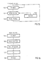
- FIG. 15 represents the flow diagram of the T FOND HV 64 program of the module 31 of FIG. 4 for the bit rate of 64 kbit / s of terminal equipment. It only monitors the states of the trunk circuits and switches.
- the T FOND HV 64 program actions and decision operations are as follows: - check whether the processing of the 1st interrupt timer, which follows the serial interrupt and which generates the corresponding rising edge of the HB HB clock for sending bits to the terminal has been carried out, according to an operation 150 denoted R HB0, the negative output of this operation looped back to its input reflecting the renewal of the operation until this timer interrupt has been processed and, if this timer interrupt has been processed, check whether the processing of the serial interrupt has been carried out, according to an operation 151 denoted SER HV 64, this processing being carried out by the SER HV 64 program described with reference to FIG.
- the T FOND 64 program is looped back on itself for its continuity.
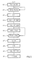
- Figure 16 shows the program flowchart SER HV 64 for handling serial interrupts for the useful speed of 64 kbit / s; It ensures the resynchronization of the HB clock on the HT clock, and the transparent transmission of data from the terminal equipment on the line.
- the synchronization of the HB clock takes place at each serial interrupt, the interval between two serial interrupts corresponding to 16 successive timer interrupts. It is performed by replacing the 16th interrupt timer with the serial interrupt that arrives.
- the program uses a counter G TIM generating the timer interrupts by counting a number N64 of pulses from the fast clock H of the processing processor. This number N64 is called the period of the counter G TIM.
- the successive actions of the SER HV 64 program are: - generate a falling edge of the clock HB, according to an action 154 denoted X HB7, - load the G TIM counter at its N64 period, according to an action 155 noted N64 ⁇ G TIM, for the theoretical generation of the 16 timer interruptions in 125 ⁇ s, - send the byte D0-D7 on the DX ports and recover the byte from the DR ports, according to an action 156 denoted D0-D7 ⁇ DX, - sample the accesses D to recover the first bit TD of a new byte according to an action 157 denoted D. - vectorize the first following timer interrupt to a program R HB0 for this program SER HV 64, according to an action 158 denoted R HB0 and explained in FIG. 17.
- the falling edge X HB7 comes from the serial interrupt which replaces the delayed timer interrupt 16. It is set on the serial interrupt for resynchronization of the HB clock on the serial interrupts and therefore on the HT clock.
- These diagrams show that the HB HV 64 clock comes from R HB and X HB programs called alternately to process successive timer interruptions. Each of these programs generates a rising or falling edge of clock HB and emits or samples the corresponding bit of data of each byte.
- the sequence of programs for processing timer interruptions results from the vectorization of timer interruptions for the bit rate considered.
- the R HB processing programs for transmitting data to the terminal are: - a program R HB0 called by the variable defined initially during the vectorization of timer interruptions for the flow considered; this program is specific for each of the possible bit rates of 64, 56, 48 kbit / s.
- the X HB processing programs for receiving data transmitted by the terminal are: - a program X HBn called routine, which is called for the first executed, XHB0 or X HB1 or X HB2 according to the flow rates, by the program R HB0 and which vectorizes the processing of the following timer interrupt at R HB n + 1, either from R HB1 or R HB2 or R HB3 to R HB7.
- the HB HV 48 clock comes from the processing of 11 timer interrupts and the serial interrupt which replaces the 12th timer interrupt
- the HB HV 56 clock comes from the processing of 13 timer interruptions and of the serial interrupt which replaces the 14th.
Landscapes
- Engineering & Computer Science (AREA)
- Computer Security & Cryptography (AREA)
- Computer Networks & Wireless Communication (AREA)
- Signal Processing (AREA)
- Time-Division Multiplex Systems (AREA)
- Radar Systems Or Details Thereof (AREA)
- Small-Scale Networks (AREA)
- Transmitters (AREA)
- Sub-Exchange Stations And Push- Button Telephones (AREA)
Applications Claiming Priority (2)
| Application Number | Priority Date | Filing Date | Title |
|---|---|---|---|
| FR8910419A FR2650717B1 (fr) | 1989-08-02 | 1989-08-02 | Transmetteur numerique synchrone |
| FR8910419 | 1989-08-02 |
Publications (2)
| Publication Number | Publication Date |
|---|---|
| EP0411529A1 true EP0411529A1 (de) | 1991-02-06 |
| EP0411529B1 EP0411529B1 (de) | 1994-08-31 |
Family
ID=9384406
Family Applications (1)
| Application Number | Title | Priority Date | Filing Date |
|---|---|---|---|
| EP90114571A Expired - Lifetime EP0411529B1 (de) | 1989-08-02 | 1990-07-30 | Synchroner digitaler Sender |
Country Status (6)
| Country | Link |
|---|---|
| US (1) | US5124976A (de) |
| EP (1) | EP0411529B1 (de) |
| AT (1) | ATE110905T1 (de) |
| DE (1) | DE69012020T2 (de) |
| ES (1) | ES2059927T3 (de) |
| FR (1) | FR2650717B1 (de) |
Cited By (1)
| Publication number | Priority date | Publication date | Assignee | Title |
|---|---|---|---|---|
| CN110661737A (zh) * | 2019-11-01 | 2020-01-07 | 深圳市度彼电子有限公司 | 距离测试设备及系统 |
Families Citing this family (14)
| Publication number | Priority date | Publication date | Assignee | Title |
|---|---|---|---|---|
| JP2543189B2 (ja) * | 1989-06-13 | 1996-10-16 | 富士通株式会社 | 構内交換機の中継台制御方式 |
| FI905698A7 (fi) * | 1990-11-19 | 1992-05-20 | Telenokia Oy | Dataoeverfoeringssystem och ett foerfarande foer kontroll av kontakt vid dataoeverfoeringssystemet. |
| FR2673787B1 (fr) * | 1991-03-08 | 1993-05-07 | Alcatel Business Systems | Procede et agencement concentrateurs en mode paquet pour terminaux de donnees desservis par un reseau rnis. |
| JPH05136758A (ja) * | 1991-11-15 | 1993-06-01 | Nec Corp | 多重速度変換装置 |
| US5530846A (en) * | 1993-12-29 | 1996-06-25 | International Business Machines Corporation | System for decoupling clock amortization from clock synchronization |
| US5970103A (en) | 1996-09-06 | 1999-10-19 | Townshend; Brent | High speed communications system for analog subscriber connections |
| JP4291410B2 (ja) * | 1994-12-09 | 2009-07-08 | ブレント タウンシェンド、 | 高速データ転送エンコーダ、デコーダ、システム、エンコード方法および復号方法 |
| JPH08255038A (ja) * | 1995-03-17 | 1996-10-01 | Nec Corp | V24/v28、v35共有インタフェース・システム |
| JPH10135875A (ja) * | 1996-10-28 | 1998-05-22 | Nec Corp | エコーキャンセラ装置 |
| US6111860A (en) * | 1997-11-03 | 2000-08-29 | Itt Manufacturing Enterprises, Inc. | Communication interface system for half duplex digital radios |
| DE102005041455A1 (de) * | 2005-08-31 | 2007-03-15 | Abb Patent Gmbh | Automatisierungstechnische Einrichtung |
| DE102005043485A1 (de) | 2005-09-13 | 2007-03-15 | Abb Patent Gmbh | Automatisierungstechnische Einrichtung |
| DE102005043481A1 (de) * | 2005-09-13 | 2007-03-15 | Abb Patent Gmbh | Automatisierungstechnische Einrichtung |
| DE102005043482A1 (de) * | 2005-09-13 | 2007-03-15 | Abb Patent Gmbh | Automatisierungstechnische Einrichtung |
Citations (1)
| Publication number | Priority date | Publication date | Assignee | Title |
|---|---|---|---|---|
| DE3204263A1 (de) * | 1981-03-31 | 1982-10-21 | Siemens AG, 1000 Berlin und 8000 München | Digitale fernmeldeendstelle als teilnehmer- und/oder vermittlungsstelle in einer digitalen fernmeldeanlage, insbesondere als endstelle fuer eine fernsprechanlage, bzw. fernsprechnebenstellenanlage |
Family Cites Families (4)
| Publication number | Priority date | Publication date | Assignee | Title |
|---|---|---|---|---|
| US4551835A (en) * | 1983-06-27 | 1985-11-05 | International Business Machines Corporation | X.21 Switching system |
| US4607364A (en) * | 1983-11-08 | 1986-08-19 | Jeffrey Neumann | Multimode data communication system |
| DE3544797A1 (de) * | 1985-12-18 | 1987-06-19 | Deutsche Bundespost | System zum gleichzeitigen betrieb mehrerer endgeraete an einer netzabschlusseinheit eines breitbandnetzes |
| DE3854231D1 (de) * | 1988-04-29 | 1995-08-31 | Ibm | Bitratenadaptionssystem für digitale Übertragungssysteme. |
-
1989
- 1989-08-02 FR FR8910419A patent/FR2650717B1/fr not_active Expired - Lifetime
-
1990
- 1990-07-30 AT AT90114571T patent/ATE110905T1/de not_active IP Right Cessation
- 1990-07-30 ES ES90114571T patent/ES2059927T3/es not_active Expired - Lifetime
- 1990-07-30 EP EP90114571A patent/EP0411529B1/de not_active Expired - Lifetime
- 1990-07-30 DE DE69012020T patent/DE69012020T2/de not_active Expired - Fee Related
- 1990-07-31 US US07/560,669 patent/US5124976A/en not_active Expired - Fee Related
Patent Citations (1)
| Publication number | Priority date | Publication date | Assignee | Title |
|---|---|---|---|---|
| DE3204263A1 (de) * | 1981-03-31 | 1982-10-21 | Siemens AG, 1000 Berlin und 8000 München | Digitale fernmeldeendstelle als teilnehmer- und/oder vermittlungsstelle in einer digitalen fernmeldeanlage, insbesondere als endstelle fuer eine fernsprechanlage, bzw. fernsprechnebenstellenanlage |
Non-Patent Citations (3)
| Title |
|---|
| COMMUTATION & TRANSMISSION, no. 4, 1985, pages 25-40, Paris, FR; M. BAUDOIN et al.: "L'autocommutateur multiservice opus 4 000" * |
| DATA COMMUNICATIONS INTERNATIONAL, vol. 18, no. 3, mars 1989, pages 85-100, Santa Clara, US; A. WEISSBERGER: "The evolving versions of ISDN's terminal adapter" * |
| IBM TECHNICAL DISCLOSURE BULLETIN, vol. 30, no. 11, avril 1988, pages 478-482, New York, US; "Electronically switchable interface circuit with multiple eia protocol drivers and receivers" * |
Cited By (1)
| Publication number | Priority date | Publication date | Assignee | Title |
|---|---|---|---|---|
| CN110661737A (zh) * | 2019-11-01 | 2020-01-07 | 深圳市度彼电子有限公司 | 距离测试设备及系统 |
Also Published As
| Publication number | Publication date |
|---|---|
| FR2650717B1 (fr) | 1991-10-04 |
| DE69012020D1 (de) | 1994-10-06 |
| EP0411529B1 (de) | 1994-08-31 |
| US5124976A (en) | 1992-06-23 |
| ATE110905T1 (de) | 1994-09-15 |
| DE69012020T2 (de) | 1994-12-22 |
| ES2059927T3 (es) | 1994-11-16 |
| FR2650717A1 (fr) | 1991-02-08 |
Similar Documents
| Publication | Publication Date | Title |
|---|---|---|
| EP0411529B1 (de) | Synchroner digitaler Sender | |
| EP0113307B1 (de) | Anpassungseinrichtung für digitale Informationsblöcke fester Länge | |
| EP0014152B1 (de) | Operator für Datenpaketvermittlungsnetz | |
| FR2655223A1 (fr) | Procede de gestion des flux dans un reseau numerique de telecommunication a integration de services, a large bande, et reseau pour le mise en óoeuvre de ce procede. | |
| FR2694828A1 (fr) | Bus d'ordinateur à transfert de paquets. | |
| CA1219386A (fr) | Systeme de multiplexage numerique temporel asynchrone a bus distribue | |
| FR2478913A1 (fr) | Concentrateur de systeme de communication pour relier plusieurs terminaux asynchrones de teleinformatique | |
| EP0094322B1 (de) | Koppler hoher Durchgangsrate zwischen einem PCM-Multiplex und einer Paketvermittlung | |
| EP0162174A1 (de) | Puffereinrichtung für ein Sprachübertragungsnetzwerk | |
| FR2467523A1 (fr) | Systeme de controle d'un reseau de connexion | |
| EP0505281B1 (de) | Endstationssynchronisierung in einem Baumnetzwerk mit mehreren Übertragungsraten und Halbduplexbetrieb | |
| FR2642245A1 (fr) | Systeme de reception et de traitement de trames hdlc transmises sur liaison mic multivoies a multiplexage temporel, notamment pour commutateur de donnees | |
| EP0120172B1 (de) | Businterfacevorrichtung für ein Datenverarbeitungssystem | |
| EP0112425A1 (de) | ZRZ-Koppelfeld unter Verwendung einer geschlossenen Schleifenverbindung | |
| EP0075247A1 (de) | Gruppe von Anschlusssätzen für ein automatisches digitales Vermittlungssystem | |
| EP0161162B1 (de) | Automatische Vermittlungsanlage mit Video-Schaltmatrix | |
| EP0178205B1 (de) | Digitales Netz mit Vielfachzugriff | |
| FR2689713A1 (fr) | Dispositif de transmission de données pour réseau à accès aléatoire, avec résolution de collision perfectionnée, et procédé correspondant. | |
| EP0101377A1 (de) | Vorrichtung für die Steuerung von Dateienübertragungen zwischen Rechnern | |
| EP0106714B1 (de) | Zugriffspunktstruktur eines Verbreitungsnetzes für Datenpakete | |
| EP0637417B1 (de) | Datenübertragungseinrichtung und verfahren für funknetz | |
| FR2693333A1 (fr) | Dispositif de recalage d'informations multiplexées. | |
| FR2459597A1 (fr) | Generateur numerique de signaux | |
| EP0250276B1 (de) | Schnittstelle zwischen einer Datenübertragungseinrichtung und mehreren Datenendeinrichtungen | |
| EP0230847B1 (de) | Paket-Multiplex-Vermittlungssystem |
Legal Events
| Date | Code | Title | Description |
|---|---|---|---|
| PUAI | Public reference made under article 153(3) epc to a published international application that has entered the european phase |
Free format text: ORIGINAL CODE: 0009012 |
|
| AK | Designated contracting states |
Kind code of ref document: A1 Designated state(s): AT BE CH DE DK ES FR GB IT LI NL SE |
|
| 17P | Request for examination filed |
Effective date: 19910729 |
|
| 17Q | First examination report despatched |
Effective date: 19931119 |
|
| GRAA | (expected) grant |
Free format text: ORIGINAL CODE: 0009210 |
|
| AK | Designated contracting states |
Kind code of ref document: B1 Designated state(s): AT BE CH DE DK ES FR GB IT LI NL SE |
|
| PG25 | Lapsed in a contracting state [announced via postgrant information from national office to epo] |
Ref country code: NL Effective date: 19940831 Ref country code: DK Effective date: 19940831 |
|
| REF | Corresponds to: |
Ref document number: 110905 Country of ref document: AT Date of ref document: 19940915 Kind code of ref document: T |
|
| REF | Corresponds to: |
Ref document number: 69012020 Country of ref document: DE Date of ref document: 19941006 |
|
| GBT | Gb: translation of ep patent filed (gb section 77(6)(a)/1977) |
Effective date: 19941010 |
|
| REG | Reference to a national code |
Ref country code: ES Ref legal event code: FG2A Ref document number: 2059927 Country of ref document: ES Kind code of ref document: T3 |
|
| ITF | It: translation for a ep patent filed | ||
| PG25 | Lapsed in a contracting state [announced via postgrant information from national office to epo] |
Ref country code: SE Effective date: 19941130 |
|
| NLV1 | Nl: lapsed or annulled due to failure to fulfill the requirements of art. 29p and 29m of the patents act | ||
| PLBE | No opposition filed within time limit |
Free format text: ORIGINAL CODE: 0009261 |
|
| STAA | Information on the status of an ep patent application or granted ep patent |
Free format text: STATUS: NO OPPOSITION FILED WITHIN TIME LIMIT |
|
| 26N | No opposition filed | ||
| PGFP | Annual fee paid to national office [announced via postgrant information from national office to epo] |
Ref country code: GB Payment date: 20000614 Year of fee payment: 11 |
|
| PGFP | Annual fee paid to national office [announced via postgrant information from national office to epo] |
Ref country code: CH Payment date: 20000616 Year of fee payment: 11 |
|
| PGFP | Annual fee paid to national office [announced via postgrant information from national office to epo] |
Ref country code: AT Payment date: 20000622 Year of fee payment: 11 |
|
| PGFP | Annual fee paid to national office [announced via postgrant information from national office to epo] |
Ref country code: FR Payment date: 20000629 Year of fee payment: 11 Ref country code: DE Payment date: 20000629 Year of fee payment: 11 |
|
| PGFP | Annual fee paid to national office [announced via postgrant information from national office to epo] |
Ref country code: BE Payment date: 20000704 Year of fee payment: 11 |
|
| PGFP | Annual fee paid to national office [announced via postgrant information from national office to epo] |
Ref country code: ES Payment date: 20000720 Year of fee payment: 11 |
|
| PG25 | Lapsed in a contracting state [announced via postgrant information from national office to epo] |
Ref country code: GB Free format text: LAPSE BECAUSE OF NON-PAYMENT OF DUE FEES Effective date: 20010730 Ref country code: AT Free format text: LAPSE BECAUSE OF NON-PAYMENT OF DUE FEES Effective date: 20010730 |
|
| PG25 | Lapsed in a contracting state [announced via postgrant information from national office to epo] |
Ref country code: LI Free format text: LAPSE BECAUSE OF NON-PAYMENT OF DUE FEES Effective date: 20010731 Ref country code: ES Free format text: LAPSE BECAUSE OF NON-PAYMENT OF DUE FEES Effective date: 20010731 Ref country code: CH Free format text: LAPSE BECAUSE OF NON-PAYMENT OF DUE FEES Effective date: 20010731 Ref country code: BE Free format text: LAPSE BECAUSE OF NON-PAYMENT OF DUE FEES Effective date: 20010731 |
|
| BERE | Be: lapsed |
Owner name: ALCATEL BUSINESS SYSTEMS Effective date: 20010731 |
|
| REG | Reference to a national code |
Ref country code: CH Ref legal event code: PL |
|
| GBPC | Gb: european patent ceased through non-payment of renewal fee |
Effective date: 20010730 |
|
| PG25 | Lapsed in a contracting state [announced via postgrant information from national office to epo] |
Ref country code: FR Free format text: LAPSE BECAUSE OF NON-PAYMENT OF DUE FEES Effective date: 20020329 |
|
| PG25 | Lapsed in a contracting state [announced via postgrant information from national office to epo] |
Ref country code: DE Free format text: LAPSE BECAUSE OF NON-PAYMENT OF DUE FEES Effective date: 20020501 |
|
| REG | Reference to a national code |
Ref country code: FR Ref legal event code: ST |
|
| REG | Reference to a national code |
Ref country code: ES Ref legal event code: FD2A Effective date: 20020810 |
|
| PG25 | Lapsed in a contracting state [announced via postgrant information from national office to epo] |
Ref country code: IT Free format text: LAPSE BECAUSE OF NON-PAYMENT OF DUE FEES;WARNING: LAPSES OF ITALIAN PATENTS WITH EFFECTIVE DATE BEFORE 2007 MAY HAVE OCCURRED AT ANY TIME BEFORE 2007. THE CORRECT EFFECTIVE DATE MAY BE DIFFERENT FROM THE ONE RECORDED. Effective date: 20050730 |