EP0412252B1 - Méthode et circuit pour le calcul d'une transformée discrète bidimensionnelle - Google Patents
Méthode et circuit pour le calcul d'une transformée discrète bidimensionnelle Download PDFInfo
- Publication number
- EP0412252B1 EP0412252B1 EP90110138A EP90110138A EP0412252B1 EP 0412252 B1 EP0412252 B1 EP 0412252B1 EP 90110138 A EP90110138 A EP 90110138A EP 90110138 A EP90110138 A EP 90110138A EP 0412252 B1 EP0412252 B1 EP 0412252B1
- Authority
- EP
- European Patent Office
- Prior art keywords
- bits
- words
- matrix
- bit
- data
- Prior art date
- Legal status (The legal status is an assumption and is not a legal conclusion. Google has not performed a legal analysis and makes no representation as to the accuracy of the status listed.)
- Expired - Lifetime
Links
Images


Classifications
-
- G—PHYSICS
- G06—COMPUTING OR CALCULATING; COUNTING
- G06F—ELECTRIC DIGITAL DATA PROCESSING
- G06F17/00—Digital computing or data processing equipment or methods, specially adapted for specific functions
- G06F17/10—Complex mathematical operations
- G06F17/14—Fourier, Walsh or analogous domain transformations, e.g. Laplace, Hilbert, Karhunen-Loeve, transforms
- G06F17/147—Discrete orthonormal transforms, e.g. discrete cosine transform, discrete sine transform, and variations therefrom, e.g. modified discrete cosine transform, integer transforms approximating the discrete cosine transform
Definitions
- the present invention refers to a system for calculating the bidimensional discrete transform in cosine, according to the preamble of claim 1. Further the invention includes also the circuits for the implementation of the said system. As is well-known, the encoding of television signals is made very efficiently by the use of the discrete transform in cosine (DCT) having dimension 8*8, or, more generally M*M, where M is a power of the number 2.
- DCT discrete transform in cosine
- the number of samples to be processed is very high (typically over 10 millions of samples per second, and for the digital format for studio it is in the order of 27 millions of samples per second) and, in particular, for the high-definition television (HDTV) the sample flow on which it is necessary to operate the DCT is higher than 100 millions per second; in this case more processors operating in parallel are used, but it is obvious the interest in a circuit that makes the bidimensional DCT at a whenever possible higher speed for reducing the number of processors to be used.
- HDTV high-definition television
- the execution of the bidimensional DCT of dimension M*M is made decomposing it into two transforms of dimension M and serial arithmetic is used for the calculation thereof, in which for the precision accuracy there are used representations of numbers with B binary ciphers, where B is usually equal to 16; it must be noticed that the words incoming into DCT and the words outgoing from the same DCT (calculation results) are under 16 bits (usually from 8 to 12 bits).
- the transfer speed of bits contained in words in serial form is double with respect to the speed of the words incoming into and outgoing from the processor DCT, which on one hand obliges to supply a processor DCT with a clock frequency doubled with respect to the frequency of incoming and outgoing words, and on the other hand to require more high performances as regards the frequency of the calculation elements, or in equivalent manner, keeping constant the speed at which the bits are processed in the inside of the processor, to limit the speed of incoming and outgoing words.
- the invention consists in the representation of the each word in the form of two serial flows (Sp and Sd) holding 8 bits, instead of a sole serial flow S of 16 bits.
- the two serial flows are made of - respectively - the bits of even positions (even flow Sp) and the ones of odd position (odd flow Sd) of the processing data.
- the elementary calculation structures adders/ subtractors
- the elementary calculation structures are organized for operating onto bit couples instead of onto single bits. In this manner, at each clock stroke it is made a processing onto a bit of even flow Sp and onto a bit of odd flow Sd.
- it is possibile to get a transfer speed of the word bits in the serial form equal to:
- the invention is applicable to the case in which it is necessary to make a dimensional transform M*M, with M having power 2, and in which the calculations are made in the serial form onto bit couples of words having a length equal to 2 Mbit.
- the invention includes also the circuits for the implementation of the considered system; some preferred fulfilment forms are recited in claims from 6 to 8.
- a bidimensional DCT can be seen as a cascade of:
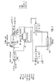
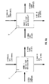
- the Figure 1 shows the block scheme of the bidimensional DCT processor; it carries out the bidimensional DCT 8 ⁇ 8, both in transmission and in reception (according to the control TXRX). According to what it has been described above, there are present two calculation blocks for carrying out the monodimensional DCT and one block for the transposition of the intermediate matrix.
- Figure 1 shows in particular the input-output signals and the control signals internal to the chip:
- the DCTR and DCTC blocks carry out the calculation of the two monodimensional DCTs.
- the transform operations are implemented according to "Fast” algorithms and they form some calculation “throttles” in cascade (in reception the order of the throttles is inverted with respect to transmission).
- the main operations made by means of the calculation throttles are: summation, subtraction, multiplication.
- serial arithmetic and interpreting the multiplication as a succession of partial summations it can be noticed how it is useful the introduction of an elementary cell that carries out the summation and subtraction operations and then can be also used for the calculation of multiplications.
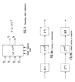
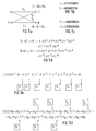
- the Figure 2 shows the scheme of an elementary adder/subtractor that works onto serialized bit couples. It represents the main block of the transform operation.
- the equation S ( ⁇ X ⁇ Y )2 -m indicates that, being given the variable quantities X and Y (positive or negative), it is made a summation or subtraction, and the result must be divided by 2 m (weighing according to 2 -m ).
- the value 2 -m is the binary weight of the current summation.
- the blocks "1" and “2" carry out the summations onto bit couples at input.
- the block "3" (exor with 3 inputs) carries out the sign extension of the summation.
- the Figure 3b shows a diagram of the summation (X + Y) 2 -4 versus time. It must be noticed as the 2i-th-bits and the (2i+1)th-bits are processed contemporaneously.
- "E” shows the sign extension of the summation (X + Y)2 -4 .
- the Figure 4b shows a diagram of the summation (X + Y)2 -3 versus time.
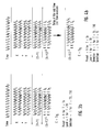
- the forming blocks are some multiplication throttles. They are made up of multiplicands (variable quantities) and multipliers (fixed quantities).
- the Figure 5a shows the calculation throttle ⁇ C1, S1 ⁇ .
- the multiplicands are in the form of bit couples entering and outgoing in a serial manner; the multiplicands ⁇ C1, S1 ⁇ are fixed numbers and during the calculation of the DCT transform corespond to the binary representation on m fractionary bits (as many as necessary) of the used sine and cosine values.
- the Figure 5c represents the corresponding ⁇ S ' 1 i , C ' 1 i ⁇ according to the ternary representation, where the value - 1 is indicated by 1.
- the Figure 5d shows the outputs Z and W as successions of summations and the Figure 5e shows the output W as succession of partial summations.
- the Figure 5f shows that the succession of partial summations is evidenced by the representation with even bits and odd bits.
- the Figure 5g represents the corresponding scheme comnpleted with the calculation of W (for getting the output Z of the throttle, a similar scheme is implemented).
- the "Round" input of the FINAL adder it forms the initial carry of the final summation.
- the initial carry should be equal to 1 in all cases at the suitable time instant.
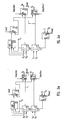
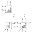
- the Figure 6a represents the principle scheme of the basical element forming the serial-parallel-serial converter: two matrix couples (MATRIX 1a, MATRIX 1b) and (MATRIX 2a, MATRIX 2b); while the MATRIX 1a loads the data in parallel, the MATRIX 1b loads the data in series (MATRIX 2a and MATRIX 2b work in similar manner in the serial-parallel conversion).
- the two matrix couples work respectively:
- the MATRIX 2b works in a similar manner, alternating its running over time with the MATRIX 2a.
- Each element of the four matrixes is a Flip-Flop with selection; the selection is controlled by a suitable control signal, having a period equal to 16 clock strokes; in particular:
- the couple (MATRIX 2a, MATRIX 2b) makes the opposite operation with respect to (MATRIX 1a, MATRIX 1b), being controlled by the signal D.
- the delay introduced into the DCT calculation is generally equal to: N ⁇ 8 + K, then D is delayed (and negated) with respect to C of K clock strokes.
- the block MEMCG exchanges the lines and columns of a matrix of 8 ⁇ 8 samples, downstream a monodimensional transform; then it carries out the transposition of a matrix.
- the running principle is similar to the principle of PARSERG; the main element is a matrix couple ( Figure 7a).
- Each element of a matrix is a generical memory element with selection; the selection is controlled by a suitable control signal having a period equal to 128 clock strokes.
- the input flows are of serial type and form the 8 vectors of the matrix (each vector is formed by 8 elements; each element of a generical vector is formed by 8 variable even bits).
- the DCT calculation is made without any scaling; but usually the DCT data are reduced in precision for allowing the transmission. Therefore it is advantageous to insert an element that makes a shift onto the transform coefficients; in particular it is advantageous the use of a scaler that multiplies by 2 -n/8 , where n is an integral number.
- the Figure 8a shows the chain of two shifts in transmission.
- the ideal inverse operation in reception is represented in Figure 8b.
Landscapes
- Physics & Mathematics (AREA)
- Engineering & Computer Science (AREA)
- General Physics & Mathematics (AREA)
- Mathematical Physics (AREA)
- Mathematical Analysis (AREA)
- Data Mining & Analysis (AREA)
- Computational Mathematics (AREA)
- Pure & Applied Mathematics (AREA)
- Mathematical Optimization (AREA)
- Theoretical Computer Science (AREA)
- Discrete Mathematics (AREA)
- Databases & Information Systems (AREA)
- Software Systems (AREA)
- General Engineering & Computer Science (AREA)
- Algebra (AREA)
- Complex Calculations (AREA)
- Compression Or Coding Systems Of Tv Signals (AREA)
- Compression, Expansion, Code Conversion, And Decoders (AREA)
Claims (6)
- Procédé pour effectuer une transformation bidimensionnelle de la dimension M*M, qui est orthogonale et séparable en deux transformations unidimensionnelles effectuées sur la base de calculs en papillon, le procédé comprenant des opérations dont des additions, des soustractions et des multiplications sur des mots d'arrivée et de départ écrits sous la forme de bits en parallèle, chacun desdits mots d'arrivée et de départ ayant une longueur maximale de 2*M bits, lesdites additions, soustractions et multiplications étant effectuées sur des données variables représentées sous la forme de mots ayant chacun une longueur de 2*M bits
caractérisé en ce que lesdites opérations d'addition et de soustraction sur lesdites données variables, par exemple sur une donnée variable


- Procédé selon la revendication 1, dans lequel seulement deux éléments de calcul sont utilisés, le premier élément étant adapté pour l'addition ou la soustraction de deux quantités variables suivie par la multiplication par 2-m, m étant un entier pair ≥ 0, et le second élément étant adapté pour l'addition ou la soustraction de deux quantités variables suivie par la multiplication par 2-n, n étant un entier impair ≥ 0, lesdits éléments de calcul ne différant qu'en ce que le second élément comprend un élément à retard pour introduire un retard d'une période d'horloge sur un seul bit de chaque paire de bits partant de l'élément de calcul.
- Procédé selon la revendication 1 ou 2, dans lequel ladite transformation est une transformation discrète en cosinus de la dimension M*M, M étant une puissance de 2.
- Procédé selon la revendication 3, dans lequel ladite transformation a la dimension 8*8 et lesdites données variables sont représentées intérieurement avec une précision de 16 bits.
- Circuit pour mettre en oeuvre le procédé selon l'une quelconque des revendications précédentes, caractérisé parun moyen pour convertir les mots d'arrivée X = {x0, x1, x2, x3, ..., x14, x15}en les faisant passer de la forme de bits en parallèle à la forme de mots X = {{x0, x1}, {x2, x3}, ..., {x14, x15}} représentés par des bits couplés à répartition en série dans le temps,un moyen pour appliquer une transformation unidimensionnelle aux lignes d'un bloc de données M*M, traiter les données sous la forme de bits à répartition en série,un moyen pour transposer de lignes en colonnes les éléments dudit bloc de données M*M,un moyen pour appliquer la transformation monodimensionnelle aux colonnes desdits blocs de données M*M, etun moyen pour convertir les paires de bits en série S = {{s0, s1}, {s2, s3}, ..., {s14, s15}} en mots sous la forme de bits en parallèle S = {s0, s1, s2, s3, ..., s14, s15}
- Circuit selon la revendication 5, mis en oeuvre sur une base en silicium et comprenantune interface d'entrée (INTIG),un convertisseur (PARSERG) pour convertir des mots d'arrivée qui sont sous la forme de bits en parallèle en les transformant en mots représentés par des paires de bits en série et pour convertir en sens inverse des mots de départ,un premier opérateur (DCTR) effectuant la transformation DCT unidimensionnelle,un moyen (MEMCG) effectuant la transposition de lignes en colonnes,un deuxième opérateur (DCTC) effectuant une transformation unidimensionnelle, etun moyen (INTOG) pour mettre à l'échelle les mots de départ.
Applications Claiming Priority (2)
| Application Number | Priority Date | Filing Date | Title |
|---|---|---|---|
| IT2142089 | 1989-07-13 | ||
| IT8921420U IT8921420V0 (it) | 1989-07-13 | 1989-07-13 | Sistema e circuito per il calcolo di trasformata discreta bidimensionale. |
Publications (3)
| Publication Number | Publication Date |
|---|---|
| EP0412252A2 EP0412252A2 (fr) | 1991-02-13 |
| EP0412252A3 EP0412252A3 (en) | 1991-07-31 |
| EP0412252B1 true EP0412252B1 (fr) | 1997-11-05 |
Family
ID=11181511
Family Applications (1)
| Application Number | Title | Priority Date | Filing Date |
|---|---|---|---|
| EP90110138A Expired - Lifetime EP0412252B1 (fr) | 1989-07-13 | 1990-05-29 | Méthode et circuit pour le calcul d'une transformée discrète bidimensionnelle |
Country Status (6)
| Country | Link |
|---|---|
| US (1) | US5197021A (fr) |
| EP (1) | EP0412252B1 (fr) |
| JP (1) | JPH03165192A (fr) |
| DE (1) | DE69031674T2 (fr) |
| ES (1) | ES2111523T3 (fr) |
| IT (1) | IT8921420V0 (fr) |
Families Citing this family (28)
| Publication number | Priority date | Publication date | Assignee | Title |
|---|---|---|---|---|
| US6336180B1 (en) | 1997-04-30 | 2002-01-01 | Canon Kabushiki Kaisha | Method, apparatus and system for managing virtual memory with virtual-physical mapping |
| US5319724A (en) * | 1990-04-19 | 1994-06-07 | Ricoh Corporation | Apparatus and method for compressing still images |
| US5664028A (en) * | 1990-04-19 | 1997-09-02 | Ricoh Corporation | Apparatus and method for compressing still images |
| FR2680259A1 (fr) * | 1991-10-09 | 1993-02-12 | Ricoh Kk | Appareil et procede de compression d'image. |
| US5410500A (en) * | 1992-02-21 | 1995-04-25 | Sony Corporation | Discrete cosine transform apparatus and inverse discrete cosine transform apparatus |
| US5313579A (en) * | 1992-06-04 | 1994-05-17 | Bell Communications Research, Inc. | B-ISDN sequencer chip device |
| KR940004467A (ko) * | 1992-08-26 | 1994-03-15 | 오오가 노리오 | 이산코사인 변환장치 및 그 역변환장치 |
| US5654910A (en) * | 1992-08-26 | 1997-08-05 | Sony Corporation | Processing method and apparatus for performing 4 ×4 discrete cosine transformation or inverse discrete cosing transformation |
| JPH06103301A (ja) * | 1992-09-17 | 1994-04-15 | Sony Corp | 8x8離散コサイン変換回路および8x8離散コサイン逆変換回路 |
| JPH06149862A (ja) * | 1992-11-13 | 1994-05-31 | Sony Corp | 行列データ乗算方法及び行列データ乗算装置 |
| US5345408A (en) * | 1993-04-19 | 1994-09-06 | Gi Corporation | Inverse discrete cosine transform processor |
| GB2302421B (en) * | 1995-03-18 | 1999-11-03 | United Microelectronics Corp | Apparatus for two-dimensional inverse discrete cosine transform |
| US5671169A (en) * | 1995-06-23 | 1997-09-23 | United Microelectronics Corporation | Apparatus for two-dimensional inverse discrete cosine transform |
| US5867601A (en) * | 1995-10-20 | 1999-02-02 | Matsushita Electric Corporation Of America | Inverse discrete cosine transform processor using parallel processing |
| US5805482A (en) * | 1995-10-20 | 1998-09-08 | Matsushita Electric Corporation Of America | Inverse discrete cosine transform processor having optimum input structure |
| US5801979A (en) * | 1995-10-20 | 1998-09-01 | Matsushita Electric Corporation Of America | Carry logic that produces a carry value from NLSBs for a ROM accumulator in an inverse discrete cosine transform processor |
| AUPO648397A0 (en) | 1997-04-30 | 1997-05-22 | Canon Information Systems Research Australia Pty Ltd | Improvements in multiprocessor architecture operation |
| AUPO647997A0 (en) * | 1997-04-30 | 1997-05-22 | Canon Information Systems Research Australia Pty Ltd | Memory controller architecture |
| US6414687B1 (en) | 1997-04-30 | 2002-07-02 | Canon Kabushiki Kaisha | Register setting-micro programming system |
| US6289138B1 (en) | 1997-04-30 | 2001-09-11 | Canon Kabushiki Kaisha | General image processor |
| US6061749A (en) * | 1997-04-30 | 2000-05-09 | Canon Kabushiki Kaisha | Transformation of a first dataword received from a FIFO into an input register and subsequent dataword from the FIFO into a normalized output dataword |
| US6507898B1 (en) | 1997-04-30 | 2003-01-14 | Canon Kabushiki Kaisha | Reconfigurable data cache controller |
| US6707463B1 (en) | 1997-04-30 | 2004-03-16 | Canon Kabushiki Kaisha | Data normalization technique |
| US6499045B1 (en) * | 1999-10-21 | 2002-12-24 | Xilinx, Inc. | Implementation of a two-dimensional wavelet transform |
| US6684235B1 (en) | 2000-11-28 | 2004-01-27 | Xilinx, Inc. | One-dimensional wavelet system and method |
| JP3830497B2 (ja) * | 2004-06-11 | 2006-10-04 | シャープ株式会社 | 半導体ウエハの製造方法及び半導体装置の製造方法 |
| GB2452103B (en) * | 2007-01-05 | 2011-08-31 | Arthrocare Corp | Electrosurgical system with suction control apparatus and system |
| US8654833B2 (en) * | 2007-09-26 | 2014-02-18 | Qualcomm Incorporated | Efficient transformation techniques for video coding |
Family Cites Families (7)
| Publication number | Priority date | Publication date | Assignee | Title |
|---|---|---|---|---|
| US4196448A (en) * | 1978-05-15 | 1980-04-01 | The United States Of America As Represented By The Secretary Of The Navy | TV bandwidth reduction system using a hybrid discrete cosine DPCM |
| US4385363A (en) * | 1978-12-15 | 1983-05-24 | Compression Labs, Inc. | Discrete cosine transformer |
| US4293920A (en) * | 1979-09-04 | 1981-10-06 | Merola Pasquale A | Two-dimensional transform processor |
| US4449194A (en) * | 1981-09-25 | 1984-05-15 | Motorola Inc. | Multiple point, discrete cosine processor |
| FR2561011B1 (fr) * | 1984-03-09 | 1986-09-12 | Cit Alcatel | Processeur de calcul d'une transformee discrete inverse du cosinus |
| IT1207346B (it) * | 1987-01-20 | 1989-05-17 | Cselt Centro Studi Lab Telecom | Sformata coseno discreta a coeffi circuito per il calcolo della tra cienti quantizzati di campioni di segnale numerico |
| US4791598A (en) * | 1987-03-24 | 1988-12-13 | Bell Communications Research, Inc. | Two-dimensional discrete cosine transform processor |
-
1989
- 1989-07-13 IT IT8921420U patent/IT8921420V0/it unknown
-
1990
- 1990-05-29 EP EP90110138A patent/EP0412252B1/fr not_active Expired - Lifetime
- 1990-05-29 ES ES90110138T patent/ES2111523T3/es not_active Expired - Lifetime
- 1990-05-29 DE DE69031674T patent/DE69031674T2/de not_active Expired - Fee Related
- 1990-07-11 US US07/551,628 patent/US5197021A/en not_active Expired - Fee Related
- 1990-07-13 JP JP2184397A patent/JPH03165192A/ja active Pending
Also Published As
| Publication number | Publication date |
|---|---|
| US5197021A (en) | 1993-03-23 |
| JPH03165192A (ja) | 1991-07-17 |
| DE69031674D1 (de) | 1997-12-11 |
| EP0412252A3 (en) | 1991-07-31 |
| ES2111523T3 (es) | 1998-03-16 |
| DE69031674T2 (de) | 1998-06-10 |
| EP0412252A2 (fr) | 1991-02-13 |
| IT8921420V0 (it) | 1989-07-13 |
Similar Documents
| Publication | Publication Date | Title |
|---|---|---|
| EP0412252B1 (fr) | Méthode et circuit pour le calcul d'une transformée discrète bidimensionnelle | |
| US5276784A (en) | 2-D discrete cosine transform circuit with reduced number of multipliers | |
| US5467131A (en) | Method and apparatus for fast digital signal decoding | |
| US6029185A (en) | Discrete cosine high-speed arithmetic unit and related arithmetic unit | |
| US5452466A (en) | Method and apparatus for preforming DCT and IDCT transforms on data signals with a preprocessor, a post-processor, and a controllable shuffle-exchange unit connected between the pre-processor and post-processor | |
| US4216475A (en) | Digital beam former | |
| US5751619A (en) | Recurrent adrithmetical computation using carry-save arithmetic | |
| US5270953A (en) | Fast convolution multiplier | |
| US3746848A (en) | Fft process and apparatus having equal delay at each stage or iteration | |
| US7020671B1 (en) | Implementation of an inverse discrete cosine transform using single instruction multiple data instructions | |
| US6052703A (en) | Method and apparatus for determining discrete cosine transforms using matrix multiplication and modified booth encoding | |
| US5831881A (en) | Method and circuit for forward/inverse discrete cosine transform (DCT/IDCT) | |
| US4853887A (en) | Binary adder having a fixed operand and parallel-serial binary multiplier incorporating such an adder | |
| Lim et al. | A serial-parallel architecture for two-dimensional discrete cosine and inverse discrete cosine transforms | |
| Buijs et al. | Implementation of a fast Fourier transform (FFT) for image processing applications | |
| Hung et al. | Compact inverse discrete cosine transform circuit for MPEG video decoding | |
| Samudrala et al. | Parallel and pipelined VLSI implementation of the new radix-2 DIT FFT algorithm | |
| Efstathiou et al. | On the modulo 2n+ 1 addition and subtraction for weighted operands | |
| US4181968A (en) | Method and apparatus for forming convolutions of two complex number sequences using the fermat number transform | |
| Jain et al. | VLSI implementation of two-dimensional DCT processor in real time for video codec | |
| JPH04282988A (ja) | データ変換装置及び方法 | |
| US4788654A (en) | Device for real time processing of digital signals by convolution | |
| US5999958A (en) | Device for computing discrete cosine transform and inverse discrete cosine transform | |
| Current | Application of quaternary logic to the design of a proposed discrete cosine transform chip | |
| US4899300A (en) | Circuit to perform a linear transformation on a digital signal |
Legal Events
| Date | Code | Title | Description |
|---|---|---|---|
| PUAI | Public reference made under article 153(3) epc to a published international application that has entered the european phase |
Free format text: ORIGINAL CODE: 0009012 |
|
| AK | Designated contracting states |
Kind code of ref document: A2 Designated state(s): BE CH DE DK ES FR GB GR LI NL SE |
|
| PUAL | Search report despatched |
Free format text: ORIGINAL CODE: 0009013 |
|
| AK | Designated contracting states |
Kind code of ref document: A3 Designated state(s): BE CH DE DK ES FR GB GR LI NL SE |
|
| 17P | Request for examination filed |
Effective date: 19920120 |
|
| RAP1 | Party data changed (applicant data changed or rights of an application transferred) |
Owner name: ALCATEL ITALIA SOCIETA PER AZIONI |
|
| 17Q | First examination report despatched |
Effective date: 19960731 |
|
| RAP1 | Party data changed (applicant data changed or rights of an application transferred) |
Owner name: ALCATEL ITALIA S.P.A. |
|
| GRAG | Despatch of communication of intention to grant |
Free format text: ORIGINAL CODE: EPIDOS AGRA |
|
| GRAH | Despatch of communication of intention to grant a patent |
Free format text: ORIGINAL CODE: EPIDOS IGRA |
|
| GRAH | Despatch of communication of intention to grant a patent |
Free format text: ORIGINAL CODE: EPIDOS IGRA |
|
| RAP1 | Party data changed (applicant data changed or rights of an application transferred) |
Owner name: ALCATEL ALSTHOM COMPAGNIE GENERALE D'ELECTRICITE |
|
| GRAA | (expected) grant |
Free format text: ORIGINAL CODE: 0009210 |
|
| AK | Designated contracting states |
Kind code of ref document: B1 Designated state(s): BE CH DE DK ES FR GB GR LI NL SE |
|
| PG25 | Lapsed in a contracting state [announced via postgrant information from national office to epo] |
Ref country code: NL Free format text: LAPSE BECAUSE OF FAILURE TO SUBMIT A TRANSLATION OF THE DESCRIPTION OR TO PAY THE FEE WITHIN THE PRESCRIBED TIME-LIMIT Effective date: 19971105 Ref country code: LI Free format text: LAPSE BECAUSE OF FAILURE TO SUBMIT A TRANSLATION OF THE DESCRIPTION OR TO PAY THE FEE WITHIN THE PRESCRIBED TIME-LIMIT Effective date: 19971105 Ref country code: GR Free format text: LAPSE BECAUSE OF FAILURE TO SUBMIT A TRANSLATION OF THE DESCRIPTION OR TO PAY THE FEE WITHIN THE PRESCRIBED TIME-LIMIT Effective date: 19971105 Ref country code: DK Free format text: LAPSE BECAUSE OF NON-PAYMENT OF DUE FEES Effective date: 19971105 Ref country code: CH Free format text: LAPSE BECAUSE OF FAILURE TO SUBMIT A TRANSLATION OF THE DESCRIPTION OR TO PAY THE FEE WITHIN THE PRESCRIBED TIME-LIMIT Effective date: 19971105 Ref country code: BE Free format text: LAPSE BECAUSE OF FAILURE TO SUBMIT A TRANSLATION OF THE DESCRIPTION OR TO PAY THE FEE WITHIN THE PRESCRIBED TIME-LIMIT Effective date: 19971105 |
|
| REG | Reference to a national code |
Ref country code: CH Ref legal event code: EP |
|
| REF | Corresponds to: |
Ref document number: 69031674 Country of ref document: DE Date of ref document: 19971211 |
|
| ET | Fr: translation filed | ||
| REG | Reference to a national code |
Ref country code: ES Ref legal event code: FG2A Ref document number: 2111523 Country of ref document: ES Kind code of ref document: T3 |
|
| NLV1 | Nl: lapsed or annulled due to failure to fulfill the requirements of art. 29p and 29m of the patents act | ||
| REG | Reference to a national code |
Ref country code: CH Ref legal event code: PL |
|
| PLBE | No opposition filed within time limit |
Free format text: ORIGINAL CODE: 0009261 |
|
| STAA | Information on the status of an ep patent application or granted ep patent |
Free format text: STATUS: NO OPPOSITION FILED WITHIN TIME LIMIT |
|
| 26N | No opposition filed | ||
| PGFP | Annual fee paid to national office [announced via postgrant information from national office to epo] |
Ref country code: GB Payment date: 19990413 Year of fee payment: 10 |
|
| PGFP | Annual fee paid to national office [announced via postgrant information from national office to epo] |
Ref country code: FR Payment date: 19990419 Year of fee payment: 10 |
|
| PGFP | Annual fee paid to national office [announced via postgrant information from national office to epo] |
Ref country code: DE Payment date: 19990420 Year of fee payment: 10 |
|
| PGFP | Annual fee paid to national office [announced via postgrant information from national office to epo] |
Ref country code: SE Payment date: 19990421 Year of fee payment: 10 |
|
| PGFP | Annual fee paid to national office [announced via postgrant information from national office to epo] |
Ref country code: ES Payment date: 19990521 Year of fee payment: 10 |
|
| PG25 | Lapsed in a contracting state [announced via postgrant information from national office to epo] |
Ref country code: GB Free format text: LAPSE BECAUSE OF NON-PAYMENT OF DUE FEES Effective date: 20000529 |
|
| PG25 | Lapsed in a contracting state [announced via postgrant information from national office to epo] |
Ref country code: SE Free format text: LAPSE BECAUSE OF NON-PAYMENT OF DUE FEES Effective date: 20000530 Ref country code: ES Free format text: THE PATENT HAS BEEN ANNULLED BY A DECISION OF A NATIONAL AUTHORITY Effective date: 20000530 |
|
| GBPC | Gb: european patent ceased through non-payment of renewal fee |
Effective date: 20000529 |
|
| EUG | Se: european patent has lapsed |
Ref document number: 90110138.6 |
|
| PG25 | Lapsed in a contracting state [announced via postgrant information from national office to epo] |
Ref country code: FR Free format text: LAPSE BECAUSE OF NON-PAYMENT OF DUE FEES Effective date: 20010131 |
|
| PG25 | Lapsed in a contracting state [announced via postgrant information from national office to epo] |
Ref country code: DE Free format text: LAPSE BECAUSE OF NON-PAYMENT OF DUE FEES Effective date: 20010301 |
|
| REG | Reference to a national code |
Ref country code: FR Ref legal event code: ST |
|
| REG | Reference to a national code |
Ref country code: ES Ref legal event code: FD2A Effective date: 20020204 |