EP0412537A2 - Procédé et appareil pour la remise en état de toiles de polissage mécano-chimique, en particulier pour disques de semi-conducteur - Google Patents
Procédé et appareil pour la remise en état de toiles de polissage mécano-chimique, en particulier pour disques de semi-conducteur Download PDFInfo
- Publication number
- EP0412537A2 EP0412537A2 EP90115269A EP90115269A EP0412537A2 EP 0412537 A2 EP0412537 A2 EP 0412537A2 EP 90115269 A EP90115269 A EP 90115269A EP 90115269 A EP90115269 A EP 90115269A EP 0412537 A2 EP0412537 A2 EP 0412537A2
- Authority
- EP
- European Patent Office
- Prior art keywords
- polishing
- polishing cloth
- treatment liquid
- base plate
- cloth
- Prior art date
- Legal status (The legal status is an assumption and is not a legal conclusion. Google has not performed a legal analysis and makes no representation as to the accuracy of the status listed.)
- Granted
Links
- 239000004744 fabric Substances 0.000 title claims abstract description 88
- 238000000034 method Methods 0.000 title claims abstract description 19
- 235000012431 wafers Nutrition 0.000 title claims abstract description 13
- 239000004065 semiconductor Substances 0.000 title claims abstract description 7
- 238000005498 polishing Methods 0.000 claims abstract description 157
- 239000007788 liquid Substances 0.000 claims abstract description 51
- 238000002360 preparation method Methods 0.000 claims abstract description 29
- 238000007517 polishing process Methods 0.000 claims abstract description 15
- 239000002585 base Substances 0.000 claims description 43
- 239000000654 additive Substances 0.000 claims description 9
- 239000007864 aqueous solution Substances 0.000 claims description 5
- 238000012545 processing Methods 0.000 claims description 5
- 239000012670 alkaline solution Substances 0.000 claims description 2
- 150000001283 organosilanols Chemical class 0.000 claims description 2
- 230000000996 additive effect Effects 0.000 claims 1
- 229910000288 alkali metal carbonate Inorganic materials 0.000 claims 1
- 150000008041 alkali metal carbonates Chemical class 0.000 claims 1
- 150000008044 alkali metal hydroxides Chemical class 0.000 claims 1
- XUIMIQQOPSSXEZ-UHFFFAOYSA-N Silicon Chemical compound [Si] XUIMIQQOPSSXEZ-UHFFFAOYSA-N 0.000 description 6
- 229910052710 silicon Inorganic materials 0.000 description 6
- 239000010703 silicon Substances 0.000 description 6
- XLYOFNOQVPJJNP-UHFFFAOYSA-N water Substances O XLYOFNOQVPJJNP-UHFFFAOYSA-N 0.000 description 6
- 239000000243 solution Substances 0.000 description 5
- 239000003795 chemical substances by application Substances 0.000 description 4
- 230000000694 effects Effects 0.000 description 4
- 239000000463 material Substances 0.000 description 4
- 229920002635 polyurethane Polymers 0.000 description 4
- 239000004814 polyurethane Substances 0.000 description 4
- OKKJLVBELUTLKV-UHFFFAOYSA-N Methanol Chemical compound OC OKKJLVBELUTLKV-UHFFFAOYSA-N 0.000 description 3
- 230000015572 biosynthetic process Effects 0.000 description 3
- 239000011248 coating agent Substances 0.000 description 3
- 238000000576 coating method Methods 0.000 description 3
- VYPSYNLAJGMNEJ-UHFFFAOYSA-N silicon dioxide Inorganic materials O=[Si]=O VYPSYNLAJGMNEJ-UHFFFAOYSA-N 0.000 description 3
- 238000012360 testing method Methods 0.000 description 3
- JBRZTFJDHDCESZ-UHFFFAOYSA-N AsGa Chemical compound [As]#[Ga] JBRZTFJDHDCESZ-UHFFFAOYSA-N 0.000 description 2
- 229910001218 Gallium arsenide Inorganic materials 0.000 description 2
- BPQQTUXANYXVAA-UHFFFAOYSA-N Orthosilicate Chemical group [O-][Si]([O-])([O-])[O-] BPQQTUXANYXVAA-UHFFFAOYSA-N 0.000 description 2
- 150000001298 alcohols Chemical class 0.000 description 2
- 150000001875 compounds Chemical class 0.000 description 2
- 230000006866 deterioration Effects 0.000 description 2
- 238000002845 discoloration Methods 0.000 description 2
- 238000004090 dissolution Methods 0.000 description 2
- 229910052732 germanium Inorganic materials 0.000 description 2
- GNPVGFCGXDBREM-UHFFFAOYSA-N germanium atom Chemical compound [Ge] GNPVGFCGXDBREM-UHFFFAOYSA-N 0.000 description 2
- WQYVRQLZKVEZGA-UHFFFAOYSA-N hypochlorite Chemical compound Cl[O-] WQYVRQLZKVEZGA-UHFFFAOYSA-N 0.000 description 2
- 238000005259 measurement Methods 0.000 description 2
- 239000012071 phase Substances 0.000 description 2
- 229920000728 polyester Polymers 0.000 description 2
- -1 polypropylene Polymers 0.000 description 2
- 229920000915 polyvinyl chloride Polymers 0.000 description 2
- 239000004800 polyvinyl chloride Substances 0.000 description 2
- BWHMMNNQKKPAPP-UHFFFAOYSA-L potassium carbonate Chemical compound [K+].[K+].[O-]C([O-])=O BWHMMNNQKKPAPP-UHFFFAOYSA-L 0.000 description 2
- 150000004760 silicates Chemical class 0.000 description 2
- 235000012239 silicon dioxide Nutrition 0.000 description 2
- 229910000838 Al alloy Inorganic materials 0.000 description 1
- QGZKDVFQNNGYKY-UHFFFAOYSA-O Ammonium Chemical compound [NH4+] QGZKDVFQNNGYKY-UHFFFAOYSA-O 0.000 description 1
- 229910052688 Gadolinium Inorganic materials 0.000 description 1
- DGAQECJNVWCQMB-PUAWFVPOSA-M Ilexoside XXIX Chemical compound C[C@@H]1CC[C@@]2(CC[C@@]3(C(=CC[C@H]4[C@]3(CC[C@@H]5[C@@]4(CC[C@@H](C5(C)C)OS(=O)(=O)[O-])C)C)[C@@H]2[C@]1(C)O)C)C(=O)O[C@H]6[C@@H]([C@H]([C@@H]([C@H](O6)CO)O)O)O.[Na+] DGAQECJNVWCQMB-PUAWFVPOSA-M 0.000 description 1
- 239000004743 Polypropylene Substances 0.000 description 1
- ZLMJMSJWJFRBEC-UHFFFAOYSA-N Potassium Chemical compound [K] ZLMJMSJWJFRBEC-UHFFFAOYSA-N 0.000 description 1
- 239000005708 Sodium hypochlorite Substances 0.000 description 1
- 229910000831 Steel Inorganic materials 0.000 description 1
- RTAQQCXQSZGOHL-UHFFFAOYSA-N Titanium Chemical compound [Ti] RTAQQCXQSZGOHL-UHFFFAOYSA-N 0.000 description 1
- 238000005299 abrasion Methods 0.000 description 1
- 230000001476 alcoholic effect Effects 0.000 description 1
- 239000003513 alkali Substances 0.000 description 1
- 229910052782 aluminium Inorganic materials 0.000 description 1
- XAGFODPZIPBFFR-UHFFFAOYSA-N aluminium Chemical compound [Al] XAGFODPZIPBFFR-UHFFFAOYSA-N 0.000 description 1
- 239000008346 aqueous phase Substances 0.000 description 1
- 230000006399 behavior Effects 0.000 description 1
- 125000004432 carbon atom Chemical group C* 0.000 description 1
- 150000004649 carbonic acid derivatives Chemical class 0.000 description 1
- 229910052681 coesite Inorganic materials 0.000 description 1
- 230000000052 comparative effect Effects 0.000 description 1
- 238000009833 condensation Methods 0.000 description 1
- 230000005494 condensation Effects 0.000 description 1
- 238000011109 contamination Methods 0.000 description 1
- 229910052906 cristobalite Inorganic materials 0.000 description 1
- 230000000593 degrading effect Effects 0.000 description 1
- 238000002474 experimental method Methods 0.000 description 1
- 239000000835 fiber Substances 0.000 description 1
- 239000002657 fibrous material Substances 0.000 description 1
- 230000009969 flowable effect Effects 0.000 description 1
- 239000002223 garnet Substances 0.000 description 1
- 239000007789 gas Substances 0.000 description 1
- 239000011521 glass Substances 0.000 description 1
- 230000002706 hydrostatic effect Effects 0.000 description 1
- 150000004679 hydroxides Chemical class 0.000 description 1
- 238000011068 loading method Methods 0.000 description 1
- 230000015654 memory Effects 0.000 description 1
- 229910052751 metal Inorganic materials 0.000 description 1
- 239000002184 metal Substances 0.000 description 1
- 150000002739 metals Chemical class 0.000 description 1
- GBMDVOWEEQVZKZ-UHFFFAOYSA-N methanol;hydrate Chemical compound O.OC GBMDVOWEEQVZKZ-UHFFFAOYSA-N 0.000 description 1
- 238000010327 methods by industry Methods 0.000 description 1
- 239000000203 mixture Substances 0.000 description 1
- 230000003287 optical effect Effects 0.000 description 1
- 230000001590 oxidative effect Effects 0.000 description 1
- 239000002245 particle Substances 0.000 description 1
- 230000035515 penetration Effects 0.000 description 1
- 239000004033 plastic Substances 0.000 description 1
- 229920003023 plastic Polymers 0.000 description 1
- 239000006223 plastic coating Substances 0.000 description 1
- 229920001155 polypropylene Polymers 0.000 description 1
- 229920001343 polytetrafluoroethylene Polymers 0.000 description 1
- 239000004810 polytetrafluoroethylene Substances 0.000 description 1
- 229910052700 potassium Inorganic materials 0.000 description 1
- 239000011591 potassium Substances 0.000 description 1
- 229910000027 potassium carbonate Inorganic materials 0.000 description 1
- 239000008213 purified water Substances 0.000 description 1
- 239000010453 quartz Substances 0.000 description 1
- 230000001172 regenerating effect Effects 0.000 description 1
- 230000002787 reinforcement Effects 0.000 description 1
- 239000000523 sample Substances 0.000 description 1
- 238000007790 scraping Methods 0.000 description 1
- SCPYDCQAZCOKTP-UHFFFAOYSA-N silanol Chemical compound [SiH3]O SCPYDCQAZCOKTP-UHFFFAOYSA-N 0.000 description 1
- 239000000377 silicon dioxide Substances 0.000 description 1
- 229910052708 sodium Inorganic materials 0.000 description 1
- 239000011734 sodium Substances 0.000 description 1
- SUKJFIGYRHOWBL-UHFFFAOYSA-N sodium hypochlorite Chemical compound [Na+].Cl[O-] SUKJFIGYRHOWBL-UHFFFAOYSA-N 0.000 description 1
- 239000007787 solid Substances 0.000 description 1
- 230000006641 stabilisation Effects 0.000 description 1
- 238000011105 stabilization Methods 0.000 description 1
- 239000010959 steel Substances 0.000 description 1
- 229910052682 stishovite Inorganic materials 0.000 description 1
- 229910052719 titanium Inorganic materials 0.000 description 1
- 239000010936 titanium Substances 0.000 description 1
- 229910052905 tridymite Inorganic materials 0.000 description 1
- WVMSIBFANXCZKT-UHFFFAOYSA-N triethyl(hydroxy)silane Chemical compound CC[Si](O)(CC)CC WVMSIBFANXCZKT-UHFFFAOYSA-N 0.000 description 1
- PQDJYEQOELDLCP-UHFFFAOYSA-N trimethylsilane Chemical compound C[SiH](C)C PQDJYEQOELDLCP-UHFFFAOYSA-N 0.000 description 1
- AAPLIUHOKVUFCC-UHFFFAOYSA-N trimethylsilanol Chemical compound C[Si](C)(C)O AAPLIUHOKVUFCC-UHFFFAOYSA-N 0.000 description 1
Images

Classifications
-
- B—PERFORMING OPERATIONS; TRANSPORTING
- B24—GRINDING; POLISHING
- B24B—MACHINES, DEVICES, OR PROCESSES FOR GRINDING OR POLISHING; DRESSING OR CONDITIONING OF ABRADING SURFACES; FEEDING OF GRINDING, POLISHING, OR LAPPING AGENTS
- B24B53/00—Devices or means for dressing or conditioning abrasive surfaces
- B24B53/017—Devices or means for dressing, cleaning or otherwise conditioning lapping tools
-
- B—PERFORMING OPERATIONS; TRANSPORTING
- B24—GRINDING; POLISHING
- B24B—MACHINES, DEVICES, OR PROCESSES FOR GRINDING OR POLISHING; DRESSING OR CONDITIONING OF ABRADING SURFACES; FEEDING OF GRINDING, POLISHING, OR LAPPING AGENTS
- B24B53/00—Devices or means for dressing or conditioning abrasive surfaces
Definitions
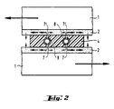
- the base plate or the outlet openings can be supplied with treatment liquid, for example, by means of a feeder tions 8 take place.
- the feed lines are expediently connected to one or more reservoirs in which the treatment liquid is placed.
- the required working pressure can be generated in various ways, for example hydrostatically by means of an elevated position of the reservoirs in relation to the base plate, or by means of pressurized gases acting on the liquid, such as compressed air, or by pumps.
- the working pressure is generally not subject to any restrictions, those pressures are generally only used in exceptional cases where the equipment, operation and safety requirements are disproportionately high.
- the line pressure provided in the usual liquid supply systems for example water pipes, is sufficient anyway.
Landscapes
- Engineering & Computer Science (AREA)
- Mechanical Engineering (AREA)
- Finish Polishing, Edge Sharpening, And Grinding By Specific Grinding Devices (AREA)
- Grinding-Machine Dressing And Accessory Apparatuses (AREA)
- Mechanical Treatment Of Semiconductor (AREA)
Applications Claiming Priority (2)
| Application Number | Priority Date | Filing Date | Title |
|---|---|---|---|
| DE3926673A DE3926673A1 (de) | 1989-08-11 | 1989-08-11 | Verfahren und vorrichtung zur poliertuchaufbereitung beim chemomechanischen polieren, insbesondere von halbleiterscheiben |
| DE3926673 | 1989-08-11 |
Publications (3)
| Publication Number | Publication Date |
|---|---|
| EP0412537A2 true EP0412537A2 (fr) | 1991-02-13 |
| EP0412537A3 EP0412537A3 (en) | 1991-04-24 |
| EP0412537B1 EP0412537B1 (fr) | 1993-10-27 |
Family
ID=6387003
Family Applications (1)
| Application Number | Title | Priority Date | Filing Date |
|---|---|---|---|
| EP90115269A Expired - Lifetime EP0412537B1 (fr) | 1989-08-11 | 1990-08-09 | Procédé et appareil pour la remise en état de toiles de polissage mécano-chimique, en particulier pour disques de semi-conducteur |
Country Status (5)
| Country | Link |
|---|---|
| US (1) | US5167667A (fr) |
| EP (1) | EP0412537B1 (fr) |
| JP (1) | JP2540080B2 (fr) |
| KR (1) | KR960015258B1 (fr) |
| DE (2) | DE3926673A1 (fr) |
Cited By (1)
| Publication number | Priority date | Publication date | Assignee | Title |
|---|---|---|---|---|
| EP0692318A1 (fr) * | 1994-06-28 | 1996-01-17 | Ebara Corporation | Procédé et dispositif de nettoyage des pièces |
Families Citing this family (17)
| Publication number | Priority date | Publication date | Assignee | Title |
|---|---|---|---|---|
| US5775983A (en) * | 1995-05-01 | 1998-07-07 | Applied Materials, Inc. | Apparatus and method for conditioning a chemical mechanical polishing pad |
| US5639311A (en) * | 1995-06-07 | 1997-06-17 | International Business Machines Corporation | Method of cleaning brushes used in post CMP semiconductor wafer cleaning operations |
| JP3778594B2 (ja) * | 1995-07-18 | 2006-05-24 | 株式会社荏原製作所 | ドレッシング方法 |
| US5938507A (en) * | 1995-10-27 | 1999-08-17 | Applied Materials, Inc. | Linear conditioner apparatus for a chemical mechanical polishing system |
| JP2862073B2 (ja) * | 1995-12-08 | 1999-02-24 | 日本電気株式会社 | ウェハー研磨方法 |
| US5704987A (en) * | 1996-01-19 | 1998-01-06 | International Business Machines Corporation | Process for removing residue from a semiconductor wafer after chemical-mechanical polishing |
| US5840202A (en) * | 1996-04-26 | 1998-11-24 | Memc Electronic Materials, Inc. | Apparatus and method for shaping polishing pads |
| US5645682A (en) * | 1996-05-28 | 1997-07-08 | Micron Technology, Inc. | Apparatus and method for conditioning a planarizing substrate used in chemical-mechanical planarization of semiconductor wafers |
| JPH1071571A (ja) * | 1996-06-27 | 1998-03-17 | Fujitsu Ltd | 研磨布、研磨布の表面処理方法、及び研磨布の洗浄方法 |
| US6379221B1 (en) | 1996-12-31 | 2002-04-30 | Applied Materials, Inc. | Method and apparatus for automatically changing a polishing pad in a chemical mechanical polishing system |
| US5957754A (en) * | 1997-08-29 | 1999-09-28 | Applied Materials, Inc. | Cavitational polishing pad conditioner |
| US6152148A (en) * | 1998-09-03 | 2000-11-28 | Honeywell, Inc. | Method for cleaning semiconductor wafers containing dielectric films |
| US6352595B1 (en) * | 1999-05-28 | 2002-03-05 | Lam Research Corporation | Method and system for cleaning a chemical mechanical polishing pad |
| DE10004578C1 (de) * | 2000-02-03 | 2001-07-26 | Wacker Siltronic Halbleitermat | Verfahren zur Herstellung einer Halbleiterscheibe mit polierter Kante |
| US7220322B1 (en) * | 2000-08-24 | 2007-05-22 | Applied Materials, Inc. | Cu CMP polishing pad cleaning |
| US6800020B1 (en) | 2000-10-02 | 2004-10-05 | Lam Research Corporation | Web-style pad conditioning system and methods for implementing the same |
| JP2006159317A (ja) * | 2004-12-03 | 2006-06-22 | Asahi Sunac Corp | 研磨パッドのドレッシング方法 |
Family Cites Families (6)
| Publication number | Priority date | Publication date | Assignee | Title |
|---|---|---|---|---|
| DE2110750A1 (de) * | 1970-03-17 | 1971-10-07 | Colgate Palmolive Co | Teppichreinigungsmittel und Verfahren zu seiner Herstellung |
| US4219333A (en) * | 1978-07-03 | 1980-08-26 | Harris Robert D | Carbonated cleaning solution |
| IT1134225B (it) * | 1980-11-12 | 1986-08-13 | Stemac Spa | Procedimento e mezzi per liberare carta abrasiva dalla polvere di levigatura depositatasi |
| JPS6017947U (ja) * | 1983-07-18 | 1985-02-06 | 東芝機械株式会社 | ポリシング装置の洗浄用ブラシ |
| JPS63283857A (ja) * | 1987-05-15 | 1988-11-21 | Asahi Chem Ind Co Ltd | 研磨布 |
| US4968380A (en) * | 1989-05-24 | 1990-11-06 | Mobil Solar Energy Corporation | System for continuously replenishing melt |
-
1989
- 1989-08-11 DE DE3926673A patent/DE3926673A1/de not_active Withdrawn
-
1990
- 1990-05-17 JP JP2125604A patent/JP2540080B2/ja not_active Expired - Lifetime
- 1990-06-05 US US07/533,479 patent/US5167667A/en not_active Expired - Fee Related
- 1990-08-09 DE DE90115269T patent/DE59003208D1/de not_active Expired - Fee Related
- 1990-08-09 EP EP90115269A patent/EP0412537B1/fr not_active Expired - Lifetime
- 1990-08-10 KR KR1019900012293A patent/KR960015258B1/ko not_active Expired - Lifetime
Cited By (2)
| Publication number | Priority date | Publication date | Assignee | Title |
|---|---|---|---|---|
| EP0692318A1 (fr) * | 1994-06-28 | 1996-01-17 | Ebara Corporation | Procédé et dispositif de nettoyage des pièces |
| US5846335A (en) * | 1994-06-28 | 1998-12-08 | Ebara Corporation | Method for cleaning workpiece |
Also Published As
| Publication number | Publication date |
|---|---|
| EP0412537B1 (fr) | 1993-10-27 |
| JPH0379268A (ja) | 1991-04-04 |
| DE3926673A1 (de) | 1991-02-14 |
| DE59003208D1 (de) | 1993-12-02 |
| EP0412537A3 (en) | 1991-04-24 |
| KR960015258B1 (ko) | 1996-11-07 |
| US5167667A (en) | 1992-12-01 |
| KR910004308A (ko) | 1991-03-28 |
| JP2540080B2 (ja) | 1996-10-02 |
Similar Documents
| Publication | Publication Date | Title |
|---|---|---|
| EP0412537B1 (fr) | Procédé et appareil pour la remise en état de toiles de polissage mécano-chimique, en particulier pour disques de semi-conducteur | |
| DE102016114798B4 (de) | Polierpad, verfahren zum herstellen eines polierpads und polierverfahren | |
| DE69937181T2 (de) | Polierschleifscheibe und substrat polierverfahren mit hilfe dieser schleifscheibe | |
| EP2102896B1 (fr) | Dispositif et procédé pour nettoyer des objets, en particulier des plaquettes minces | |
| DE69518202T2 (de) | Verfahren und Vorrichtung zum Oberflächenschleifen eines Werkstücks | |
| EP2218004B1 (fr) | Dispositif et procédé de nettoyage d'objets | |
| DE112011100688T5 (de) | Verfahren zum Herstellen eines Halbleiterwafers | |
| DE1621473A1 (de) | Verfahren zum Polieren von Halbleiteroberflaechen,insbesondere von Oberflaechen von Siliciumkoerpern und Vorrichtung zum Durchfuehren des Verfahrens | |
| DE102013212617A1 (de) | Vorrichtung zur Aufbringung von Schleifkörnern | |
| DE102017202099A1 (de) | Verfahren und vorrichtung zum erstellen dreidimensionaler zylindrischer objekte | |
| DE60307588T2 (de) | Drahtsägevorrichtung | |
| DE2007865C2 (de) | Verfahren und Vorrichtung zum Polieren einer Siliciumoberfläche | |
| DE3148957C2 (de) | Verfahren zum Herstellen rückseitig oberflächengestörter Halbleiterscheiben | |
| EP2458626A1 (fr) | Dispositif de nettoyage à retenue et procédé de nettoyage par section de tranches de silicium sciées | |
| DE69913476T2 (de) | Polierverfahren und vorrichtung | |
| EP2153960A2 (fr) | Support, procédé et dispositif de fabrication de tranches de silicium, ainsi que l'utilisation de la tranche de silicium fabriquée | |
| EP1129823B1 (fr) | Procédé de régénération de plaquettes de semiconducteurs | |
| DE3033944A1 (de) | Laeppvorrichtung fuer duenne plaettchen und aufspannvorrichtung fuer dieselben als teil der laeppvorrichtung | |
| DE2606522C2 (de) | Verfahren und Vorrichtung zum Kennzeichnen von Metall | |
| DE2637827C2 (fr) | ||
| DE1917371C3 (de) | Verfahren zur elektrolytischen Herstellung von glatten, dichten Metallschichten | |
| DE3336593C1 (de) | Verfahren zum Herstellen eines zahnrad-,zahnstangen- oder schneckenfoermigen Werkzeugs zum Feinbearbeiten der Zahnflanken von insbesondere gehaerteten Zahnraedern | |
| DE69606669T2 (de) | Vorrichtung zum abrichten eines polierkissen | |
| DE69802630T2 (de) | Verfahren und Vorrichtung zur Oberflächenbehandlung von Flachdruckplattenträger und Schleifmaschine zum Schleifen der Behandlungsbürste | |
| EP1992458A1 (fr) | Lame destinée à l'utilisation d'une machine destinée à couper ou estampiller des piles de feuilles ainsi que procédé de traitement d'une telle lame |
Legal Events
| Date | Code | Title | Description |
|---|---|---|---|
| PUAI | Public reference made under article 153(3) epc to a published international application that has entered the european phase |
Free format text: ORIGINAL CODE: 0009012 |
|
| 17P | Request for examination filed |
Effective date: 19900809 |
|
| AK | Designated contracting states |
Kind code of ref document: A2 Designated state(s): DE GB IT |
|
| PUAL | Search report despatched |
Free format text: ORIGINAL CODE: 0009013 |
|
| AK | Designated contracting states |
Kind code of ref document: A3 Designated state(s): DE GB IT |
|
| 17Q | First examination report despatched |
Effective date: 19930208 |
|
| ITF | It: translation for a ep patent filed | ||
| GRAA | (expected) grant |
Free format text: ORIGINAL CODE: 0009210 |
|
| AK | Designated contracting states |
Kind code of ref document: B1 Designated state(s): DE GB IT |
|
| REF | Corresponds to: |
Ref document number: 59003208 Country of ref document: DE Date of ref document: 19931202 |
|
| GBT | Gb: translation of ep patent filed (gb section 77(6)(a)/1977) |
Effective date: 19931202 |
|
| PLBE | No opposition filed within time limit |
Free format text: ORIGINAL CODE: 0009261 |
|
| STAA | Information on the status of an ep patent application or granted ep patent |
Free format text: STATUS: NO OPPOSITION FILED WITHIN TIME LIMIT |
|
| 26N | No opposition filed | ||
| REG | Reference to a national code |
Ref country code: GB Ref legal event code: 732E |
|
| PGFP | Annual fee paid to national office [announced via postgrant information from national office to epo] |
Ref country code: GB Payment date: 19960724 Year of fee payment: 7 |
|
| PGFP | Annual fee paid to national office [announced via postgrant information from national office to epo] |
Ref country code: DE Payment date: 19960905 Year of fee payment: 7 |
|
| PG25 | Lapsed in a contracting state [announced via postgrant information from national office to epo] |
Ref country code: GB Free format text: LAPSE BECAUSE OF NON-PAYMENT OF DUE FEES Effective date: 19970809 |
|
| GBPC | Gb: european patent ceased through non-payment of renewal fee |
Effective date: 19970809 |
|
| PG25 | Lapsed in a contracting state [announced via postgrant information from national office to epo] |
Ref country code: DE Free format text: LAPSE BECAUSE OF NON-PAYMENT OF DUE FEES Effective date: 19980501 |
|
| PG25 | Lapsed in a contracting state [announced via postgrant information from national office to epo] |
Ref country code: IT Free format text: LAPSE BECAUSE OF NON-PAYMENT OF DUE FEES;WARNING: LAPSES OF ITALIAN PATENTS WITH EFFECTIVE DATE BEFORE 2007 MAY HAVE OCCURRED AT ANY TIME BEFORE 2007. THE CORRECT EFFECTIVE DATE MAY BE DIFFERENT FROM THE ONE RECORDED. Effective date: 20050809 |