EP0412921A2 - Dünnfilmtransistor-Flüssigkristall-Anzeigevorrichtung mit optischen Interferenz-Farbfiltern - Google Patents
Dünnfilmtransistor-Flüssigkristall-Anzeigevorrichtung mit optischen Interferenz-Farbfiltern Download PDFInfo
- Publication number
- EP0412921A2 EP0412921A2 EP90480086A EP90480086A EP0412921A2 EP 0412921 A2 EP0412921 A2 EP 0412921A2 EP 90480086 A EP90480086 A EP 90480086A EP 90480086 A EP90480086 A EP 90480086A EP 0412921 A2 EP0412921 A2 EP 0412921A2
- Authority
- EP
- European Patent Office
- Prior art keywords
- liquid crystal
- color
- crystal display
- pel
- thin film
- Prior art date
- Legal status (The legal status is an assumption and is not a legal conclusion. Google has not performed a legal analysis and makes no representation as to the accuracy of the status listed.)
- Granted
Links
Images


Classifications
-
- G—PHYSICS
- G02—OPTICS
- G02F—OPTICAL DEVICES OR ARRANGEMENTS FOR THE CONTROL OF LIGHT BY MODIFICATION OF THE OPTICAL PROPERTIES OF THE MEDIA OF THE ELEMENTS INVOLVED THEREIN; NON-LINEAR OPTICS; FREQUENCY-CHANGING OF LIGHT; OPTICAL LOGIC ELEMENTS; OPTICAL ANALOGUE/DIGITAL CONVERTERS
- G02F1/00—Devices or arrangements for the control of the intensity, colour, phase, polarisation or direction of light arriving from an independent light source, e.g. switching, gating or modulating; Non-linear optics
- G02F1/01—Devices or arrangements for the control of the intensity, colour, phase, polarisation or direction of light arriving from an independent light source, e.g. switching, gating or modulating; Non-linear optics for the control of the intensity, phase, polarisation or colour
- G02F1/13—Devices or arrangements for the control of the intensity, colour, phase, polarisation or direction of light arriving from an independent light source, e.g. switching, gating or modulating; Non-linear optics for the control of the intensity, phase, polarisation or colour based on liquid crystals, e.g. single liquid crystal display cells
- G02F1/133—Constructional arrangements; Operation of liquid crystal cells; Circuit arrangements
- G02F1/1333—Constructional arrangements; Manufacturing methods
- G02F1/1335—Structural association of cells with optical devices, e.g. polarisers or reflectors
- G02F1/133509—Filters, e.g. light shielding masks
- G02F1/133514—Colour filters
- G02F1/133516—Methods for their manufacture, e.g. printing, electro-deposition or photolithography
-
- G—PHYSICS
- G02—OPTICS
- G02F—OPTICAL DEVICES OR ARRANGEMENTS FOR THE CONTROL OF LIGHT BY MODIFICATION OF THE OPTICAL PROPERTIES OF THE MEDIA OF THE ELEMENTS INVOLVED THEREIN; NON-LINEAR OPTICS; FREQUENCY-CHANGING OF LIGHT; OPTICAL LOGIC ELEMENTS; OPTICAL ANALOGUE/DIGITAL CONVERTERS
- G02F1/00—Devices or arrangements for the control of the intensity, colour, phase, polarisation or direction of light arriving from an independent light source, e.g. switching, gating or modulating; Non-linear optics
- G02F1/01—Devices or arrangements for the control of the intensity, colour, phase, polarisation or direction of light arriving from an independent light source, e.g. switching, gating or modulating; Non-linear optics for the control of the intensity, phase, polarisation or colour
- G02F1/13—Devices or arrangements for the control of the intensity, colour, phase, polarisation or direction of light arriving from an independent light source, e.g. switching, gating or modulating; Non-linear optics for the control of the intensity, phase, polarisation or colour based on liquid crystals, e.g. single liquid crystal display cells
- G02F1/133—Constructional arrangements; Operation of liquid crystal cells; Circuit arrangements
- G02F1/1333—Constructional arrangements; Manufacturing methods
- G02F1/1335—Structural association of cells with optical devices, e.g. polarisers or reflectors
- G02F1/133509—Filters, e.g. light shielding masks
- G02F1/133514—Colour filters
- G02F1/133521—Interference filters
-
- G—PHYSICS
- G02—OPTICS
- G02F—OPTICAL DEVICES OR ARRANGEMENTS FOR THE CONTROL OF LIGHT BY MODIFICATION OF THE OPTICAL PROPERTIES OF THE MEDIA OF THE ELEMENTS INVOLVED THEREIN; NON-LINEAR OPTICS; FREQUENCY-CHANGING OF LIGHT; OPTICAL LOGIC ELEMENTS; OPTICAL ANALOGUE/DIGITAL CONVERTERS
- G02F1/00—Devices or arrangements for the control of the intensity, colour, phase, polarisation or direction of light arriving from an independent light source, e.g. switching, gating or modulating; Non-linear optics
- G02F1/01—Devices or arrangements for the control of the intensity, colour, phase, polarisation or direction of light arriving from an independent light source, e.g. switching, gating or modulating; Non-linear optics for the control of the intensity, phase, polarisation or colour
- G02F1/13—Devices or arrangements for the control of the intensity, colour, phase, polarisation or direction of light arriving from an independent light source, e.g. switching, gating or modulating; Non-linear optics for the control of the intensity, phase, polarisation or colour based on liquid crystals, e.g. single liquid crystal display cells
- G02F1/133—Constructional arrangements; Operation of liquid crystal cells; Circuit arrangements
- G02F1/136—Liquid crystal cells structurally associated with a semi-conducting layer or substrate, e.g. cells forming part of an integrated circuit
- G02F1/1362—Active matrix addressed cells
- G02F1/1368—Active matrix addressed cells in which the switching element is a three-electrode device
Definitions
- the present invention relates to liquid crystal displays and more particularly to a thin film transistor liquid crystal display device and the method of manufacturing such a device.
- Thin film transistor liquid crystal display (TFT LCD) technology has been developed as a successor to cathode ray tube technology for color display computer terminals.
- Liquid crystal displays with a given display screen area occupy a smaller volume than cathode ray tube devices with the same screen area. This is considered commercially significant, because the smaller liquid crystal display has a smaller footprint. That is, it occupies less area on a user's desk or terminal stand.
- Liquid crystal display devices may also have lower power requirements than corresponding cathode ray tube devices. This is because the operating voltages of liquid crystal devices are considerably lower than the operating voltages of cathode ray tube devices. These characteristics are not only desirable for computer terminals but are also desirable for televisions, video displays, and a variety of other electronic devices.
- color liquid crystal display devices While different types of color liquid crystal display devices exist, such devices generally include two spaced panels which define a sealed cavity filled with a liquid crystal display material. A transparent common electrode is formed inside the defined cavity on one of the glass panels. Individual electrodes, also on the inside of the defined cavity, are formed on the other glass panel. Each of the individual electrodes has a surface area corresponding to the area of one, or part of one, picture element or pel. Each pel is too small to be easily seen by the unaided human eye. If the device is to have color capabilities, it must also include color filters with red, green, and blue color areas. Each color area is aligned with one of the electrodes. Each set of red, green, and blue color areas is grouped into a triad, repetitive stripes, or other consistent pattern within the pel.
- each of the individual electrodes can be addressed by means of a thin film transistor.
- one or more of the pel electrodes is energized during the display operation to allow full light, no light, or partial light to be transmitted through the color filter area associated with that pel electrode.
- the image perceived by the user is a blending of colors formed by the transmission of light through adjacent color filter areas.
- the display may be backlighted by locating a light source on the opposite side of the display, away from the viewer.
- the display may include a reflective layer at its rear surface and rely on the light source located on the same side of the display as the viewer.
- Color filters for use on such devices have been fabricated using a number of different approaches.
- One approach has been to spin or deposit a light sensitized adhesive film onto the glass panel. The film is then patterned in three sequential steps. During each step, dye of a specific color is applied to predetermined regions of the film.
- organic pigments are deposited by vacuum evaporation. These pigments are then patterned by conventional lift-off techniques.
- a dyed and patterned stretched film material is used to create an internal color polarizing filter.
- each of these approaches has certain drawbacks. Most involve polymer deposition and photopatterning techniques which are relatively expensive and difficult to perform with the necessary precision. This is especially true when the devices are manufactured on a volume basis. Also, each creates a color filter film which is located between the transparent common electrode and the individually addressable pel electrodes (referred to as the gap of the device). To increase optical density (or color intensity) of color filters made by the above described approaches, the thickness of the color filter film may be increased. However, increasing the filter film thickness also increases the spacing between the transparent common electrode and the individually addressable pel electrodes. The increased spacing causes the gap and associated LCD thickness to be more nonuniform which results in nonuniform electrical characteristics of the LCD.
- TFT Thin Film Transistors
- Still another approach to making TFT LCDs uses photosensitive emulsion layers.
- a liquid crystal shutter device is used to sequentially expose predetermined areas of the photosensitive emulsion layers while the layers are flooded with light having the specific color.
- Three differently colored regions are formed by sequentially energizing three different groups of pel electrodes through associated thin film transistors.
- the latent images produced in the photosensitive emulsion layer are developed and the film is laminated to a glass substrate to form a multicolored filter.
- the present invention is an improved thin film transistor liquid crystal display with color capabilities. Interference film and printing technology are employed in the fabrication of the display to simplify the task of aligning pel electrodes with associated color regions in the color filter layer.
- This liquid crystal display device is of the type having spaced front and rear glass panels, a transparent electrode layer, and an array of individually addressable pel electrodes separated from the transparent electrode layer by a cavity filled with liquid crystal material.
- the improvement comprises a color filter layer comprised of an array of interference films.
- the filter layer is an array of color filters formed by printing a pattern in sensitized adhesive on a glass panel and selectively transferring interference color films to the adhesive pattern.
- the color filters fabricated with interference film techniques can be produced to a high resolution, do not require processing of the filter itself on the glass, and are stable at high temperatures. Therefore, less difficulty is expected in achieving volume production registration between the color regions in the color filter layer and the pel electrodes. Additionally, the color filter may be processed with any desired uniform hue and intensity without affecting the registration of the filters to the pel electrodes.
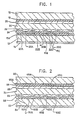
- Figure 1 is a partial cross section of a thin film transistor liquid crystal display which can be fabricated in accordance with the present invention.
- the display includes two transparent plates, 10 and 12, which are typically glass panels, a polarizing filter 14, a transparent common electrode 18, and a plurality of0C, etc.
- the pel electrodes may be individually addressed or energized through associated thin film transistors 22A, 22B, 22C, etc.
- the pel electrodes and thin film transistors are deposited directly on the filter layer with color elements 15A 15B, and 15C, details of which are provided below.
- the pel electrodes and thin film transistors are covered by a layer of insulating material 24, which is in turn, covered by an alignment film 26.
- a second alignment film 28 is deposited on the transparent common electrode 18.
- the space between the alignment films 26 and 28 is a cavity 30 which is filled with a liquid crystal material.
- the glass plates, 10 and 12, define another cavity in which the LCD material with the alignment films 26 and 28 in combination with the pel electrodes and the thin film transistors are placed.
- the polarizing filter is typically attached to one of the glass plates.
- the color filter layer is unique in that it is an interference film made of an inorganic material and transferred to a glass panel 12 using film transfer technology. This allows thin film transistors to be directly placed on the color filters to reduce registration errors.
- the interference film is formed on a substrate which is a flexible membrane, usually plastic, that has been coated with a releasable layer so that the membrane can be separated from the interference film.
- the substrate, formed by the membrane being coated with the releasable layer is typically manufactured on a continuous basis in a vacuum roll coating machine.
- the interference film is comprised of layers of thin film dielectric and metal materials. These dielectric and metal materials are blanket deposited on the substrate in the form of a Fabry Perot Optical Interference filter with the spacer layer thickness of the filter adjusted to provide the particular color desired for one of the electrodes.
- the filters can be fabricated from a variety of refractory inorganic evaporated or sputtered thin films.
- the filter typically consists of three layers, a second layer interposed between a first and third layer.
- the first and third layers are highly reflecting, slightly transmitting films such as silver.
- the second or spacer layer is a dielectric layer, such .as zinc-sulfide (ZnS).
- ZnS zinc-sulfide
- the thickness of the spacer layer determines the wavelength of the output light and hence the color.
- High index of refraction dielectric spacer layers are normally used to reduce the dependency of the transmission wavelength on the incidence angle of light.
- the reflecting layers should have reflectivity close to unity.
- the reflecting layers can be made of dielectric films, similar to the spacer layer, because reflectivity of a layer is increased when a medium of high index of refraction has embedded within it a film of low index of refraction. Therefore, high reflectivity films can be made from alternating layers of low and high index of refraction dielectrics. The result of this is that alternating layers of materials such as titanium dioxide and silicon dioxide can be used to manufacture the entire filter.
- the groups of dielectric and metal layers are deposited on a releasable layer to form the individual color filters associated with the pel array.
- Each repeatable segment of the pel array has three color filters associated with it.
- a first filter that corresponds to a first part of the pel array and to one color is deposited on a first substrate.
- a second filter that corresponds to a second part of the pel array and to a second color is deposited on a second substrate.
- a third filter that corresponds to a third part of the pel array and to a third color is deposited on a third substrate.
- a pattern of adhesive that corresponds to the pattern of filters of one color is then applied to the glass member 12.
- a number of adhesives are practical for use in this invention and are also well known, such as, heat activated adhesives, ultraviolet light initiated adhesives, or optical cements.
- the adhesive is patterned by printing or conventional photolithographic techniques.
- An interference film capable of producing the one color and having a releasable substrate backing is then laminated to the glass member by the adhesive.
- the adhesive is cured, and the flexible membrane substrate is then physically peeled away or separated from the color filters. This physical separation has two results. First, the substrate backing peels away from the interference film in the area of the interference film which is laminated onto the glass member 12 by the adhesive.
- the interference film remains on the substrate backing.
- the physical peeling away or separation breaks the interference film adhering to the substrate backing away from the interference film adhering to the glass member 12.
- the releasable film adheres to the interference film strongly enough so that the interference film itself will break before the releasable film will release the interference film from the substrate backing. Additionally, the releasable film will be weaker than the adhesive securing the interference film to the glass member 12. This results in the substrate backing peeling away from the interference film without the interference film being pulled from the surface of the glass member 12.
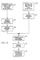
- the Transfer Color Filter Layer to Glass Panel process 80 includes the patterning of one color inorganic films on the releasable layer of the substrate 81, patterning the adhesive on the glass panel 82, aligning and laminating the color filter to the glass panel 83, and removing the substrate 84.
- the transfer process 80 of laminating the color filters to the glass member is used two more times to laminate second and third colors to the glass panel along with the first color.
- the process is repeated with the second and third patterned adhesive layers and second and third interference films on releasable substrates.
- Each substrate places one color filter within each repeatable segment of the pel array on the glass member. The location of each color filter is determined by the location of the printed adhesive.
- the resulting color filter pattern is shown in Figure 1 and comprises elements 15A, 15B, and 15C.
- the ability to make small patterns of adhesive through printing or conventional lithography is especially useful in reducing the size of the color filter to approximately that of the TFT and pel electrode. This is because once the filter is in place on the glass, the transistor and electrode fabrication, which is always much more dimensionally accurate than the color filter fabrication, will be aligned to the color filter. The alignment order is inverted from the conventional order of aligning the filter to the transistors and electrodes. This alignment is facilitated by alignment marks fabricated on the glass member from the interference film transfer process. Since the filter itself is dimensionally accurate and stable (with respect to heat and other processing) because of its inorganic nature, the color filter size can be correspondingly reduced with the ability to pattern the adhesive.
- FIG. 2 An alternative embodiment of the invention is shown in Figure 2.
- the alternative embodiment includes basically the same components as the embodiment shown in Figure 1, but the color filter layer is located in a different place. More specifically, the device shown in Figure 2 has a transparent front plate 50 which is typically glass, a transparent rear plate 52 also typically glass, a polarizing filter 54, a transparent common electrode layer 58, and an array of individually addressable pel electrodes, 60A, 60B, and 60C etc., with associated thin film transistors 62A, 62B, and 62C, etc. The pel electrodes and thin film transistors are coated with a layer 55 of insulating material. An alignment film 56 covers the insulating layer 55. A second alignment film 68 is deposited on the common electrode layer 58. The alignment films define the cavity 70 which contains the liquid crystal material.
- the filter layer comprising filter elements 65A, 65B, and 65C, etc. is applied to the front glass panel 50 beneath the common electrode layer 58.
- This embodiment does not take advantage of the alignment improvements of the embodiment in Figure 1 because the transistors are not aligned to and placed on the color filter already in place.
- the nature of the color filter material allows it to be used in configurations such as Figure 2 which still allows for better dimensional accuracy of the color filter.
- the relative positions of the color filter layer and the common electrode layer 58 can be interchanged.
- Figure 3 generally illustrates the specific operations that must be carried out in fabricating the device shown in Figure 1.
- separate and independent operations are used to form the subassemblies associated with the front and rear glass panels.
- color filters are transferred to the rear glass panel and are permanently fixed in place by the transfer process 80.
- the transfer process 80 described earlier and detailed in Figure 4, is repeated once for each color used in the color filter array, which is typically three times.
- the pel electrodes and thin film transistors can be deposited 86 directly on the color filter layer.
- the alignment film is then deposited 88 to complete the rear glass panel subassembly.
- the front glass panel subassembly is fabricated separately from the rear glass panel subassembly.
- the common electrode layer for the display device is formed on the front glass panel 90 and is covered by another alignment film to complete the front glass panel subassembly 92.
- the front and rear subassemblies are then aligned and assembled 94 with respect to each other, forming a cavity for the liquid crystal display material.
- the liquid crystal display material is then added and the cavity sealed 96.
- the driver electronics are subsequently connected to the TFT electrodes 98 and the display screen is complete.
- the alternative embodiment of the display device is fabricated according to the steps shown in Figure 5.
- the color filter layer is transferred 80 (given in more detail in Figure 4) to the front glass panel 50.
- the transparent common electrode layer 58 is then deposited 104 over the color filter layer.
- an alignment film 68 is placed 106 over the combination of the color filter film and the common electrode layer.
- the rear glass panel 52 has pel electrodes and TFTs deposited directly on it 108. This combination is then covered 110 with another alignment film 56. The front and rear glass panels are then aligned and assembled with respect to each other 112 forming a cavity 70 for the liquid crystal display material. The liquid crystal display material is then added and the cavity sealed 114. The driver electronics are subsequently connected 116 to the TFTs and electrodes to complete the display screen.
Landscapes
- Physics & Mathematics (AREA)
- Nonlinear Science (AREA)
- Engineering & Computer Science (AREA)
- Manufacturing & Machinery (AREA)
- Mathematical Physics (AREA)
- Chemical & Material Sciences (AREA)
- Crystallography & Structural Chemistry (AREA)
- General Physics & Mathematics (AREA)
- Optics & Photonics (AREA)
- Liquid Crystal (AREA)
- Optical Filters (AREA)
Applications Claiming Priority (2)
| Application Number | Priority Date | Filing Date | Title |
|---|---|---|---|
| US07/392,818 US5058997A (en) | 1989-08-11 | 1989-08-11 | Tft lcd with optical interference color filters |
| US392818 | 1989-08-11 |
Publications (3)
| Publication Number | Publication Date |
|---|---|
| EP0412921A2 true EP0412921A2 (de) | 1991-02-13 |
| EP0412921A3 EP0412921A3 (en) | 1991-11-06 |
| EP0412921B1 EP0412921B1 (de) | 1995-03-29 |
Family
ID=23552113
Family Applications (1)
| Application Number | Title | Priority Date | Filing Date |
|---|---|---|---|
| EP90480086A Expired - Lifetime EP0412921B1 (de) | 1989-08-11 | 1990-06-19 | Dünnfilmtransistor-Flüssigkristall-Anzeigevorrichtung mit optischen Interferenz-Farbfiltern |
Country Status (4)
| Country | Link |
|---|---|
| US (1) | US5058997A (de) |
| EP (1) | EP0412921B1 (de) |
| JP (1) | JPH0372322A (de) |
| DE (1) | DE69018157T2 (de) |
Cited By (6)
| Publication number | Priority date | Publication date | Assignee | Title |
|---|---|---|---|---|
| EP0716335A3 (de) * | 1994-12-08 | 1996-11-27 | Canon Kk | Anzeigetafel mit polymerdispergiertem Flüssigkristall |
| US5721596A (en) * | 1995-09-14 | 1998-02-24 | Canon Kabushiki Kaisha | Liquid crystal display device |
| EP0903613A1 (de) * | 1997-09-17 | 1999-03-24 | Matsushita Electric Industrial Co., Ltd. | Reflektive Flüssigkristall-Anzeigevorrichtung |
| WO1999021708A1 (en) * | 1997-10-24 | 1999-05-06 | Agfa-Gevaert Naamloze Vennootschap | Use of glass laminate as a substrate in semiconductor devices |
| EP1122794A2 (de) | 2000-02-01 | 2001-08-08 | Semiconductor Energy Laboratory Co., Ltd. | Halbleitervorrichtung und Herstellungsverfahren |
| CN102662299A (zh) * | 2010-10-26 | 2012-09-12 | 精工爱普生株式会社 | 投影型显示装置以及光学单元 |
Families Citing this family (26)
| Publication number | Priority date | Publication date | Assignee | Title |
|---|---|---|---|---|
| GB2235326A (en) * | 1989-08-16 | 1991-02-27 | Philips Electronic Associated | Active matrix liquid crystal colour display devices |
| US5246803A (en) * | 1990-07-23 | 1993-09-21 | Eastman Kodak Company | Patterned dichroic filters for solid state electronic image sensors |
| US6511187B1 (en) | 1992-02-20 | 2003-01-28 | Kopin Corporation | Method of fabricating a matrix display system |
| JPH06242441A (ja) * | 1992-12-22 | 1994-09-02 | Canon Inc | 光源装置及び該装置を備える表示装置 |
| US5463484A (en) * | 1993-10-29 | 1995-10-31 | Brody; Thomas P. | Method for manufacturing laminated U V-sensitive color filters for liquid crystal displays |
| JP3364081B2 (ja) * | 1995-02-16 | 2003-01-08 | 株式会社半導体エネルギー研究所 | 半導体装置の作製方法 |
| US5751388A (en) * | 1995-04-07 | 1998-05-12 | Honeywell Inc. | High efficiency polarized display |
| JP3112393B2 (ja) * | 1995-05-25 | 2000-11-27 | シャープ株式会社 | カラー表示装置 |
| JP3368110B2 (ja) | 1995-08-01 | 2003-01-20 | キヤノン株式会社 | 光源装置及び光学機器 |
| JP3234854B2 (ja) * | 1995-08-28 | 2001-12-04 | アルプス電気株式会社 | 多層膜フィルタ及びその製造方法 |
| US5645963A (en) * | 1995-11-20 | 1997-07-08 | Minnesota Mining And Manufacturing Company | Method for making color filter elements using laminable colored photosensitive materials |
| US6124908A (en) * | 1996-06-10 | 2000-09-26 | Minolta Co., Ltd. | Liquid crystal element |
| KR100471766B1 (ko) * | 1997-08-25 | 2005-07-18 | 삼성전자주식회사 | 반도체장치의제조장치 |
| US6669803B1 (en) * | 1997-10-03 | 2003-12-30 | Digital Optics Corp. | Simultaneous provision of controlled height bonding material at a wafer level and associated structures |
| JP3723336B2 (ja) * | 1997-11-18 | 2005-12-07 | 三洋電機株式会社 | 液晶表示装置 |
| US6221543B1 (en) | 1999-05-14 | 2001-04-24 | 3M Innovatives Properties | Process for making active substrates for color displays |
| KR100604717B1 (ko) * | 1999-07-08 | 2006-07-28 | 엘지.필립스 엘시디 주식회사 | 액정 표시장치 제조방법 및 그 제조방법에 따른 액정표시장치 |
| JP3538073B2 (ja) * | 1999-07-29 | 2004-06-14 | Nec液晶テクノロジー株式会社 | Tftを搭載する基板側に色層を有するアクティブマトリクス型液晶表示装置及びその製造方法 |
| JP2001209038A (ja) * | 1999-11-17 | 2001-08-03 | Nippon Sheet Glass Co Ltd | 液晶表示素子用基板 |
| US7579203B2 (en) * | 2000-04-25 | 2009-08-25 | Semiconductor Energy Laboratory Co., Ltd. | Light emitting device |
| US20030170423A1 (en) * | 2002-01-25 | 2003-09-11 | Fuji Photo Film Co., Ltd. | Method of producing pattern member, apparatus of producing pattern member, and pattern member |
| US7184106B2 (en) * | 2004-02-26 | 2007-02-27 | Au Optronics Corporation | Dielectric reflector for amorphous silicon crystallization |
| KR101183374B1 (ko) * | 2005-06-27 | 2012-09-21 | 엘지디스플레이 주식회사 | 액정표시장치 및 그 제조방법 |
| US20070252928A1 (en) * | 2006-04-28 | 2007-11-01 | Toppan Printing Co., Ltd. | Structure, transmission type liquid crystal display, reflection type display and manufacturing method thereof |
| FR2946435B1 (fr) * | 2009-06-04 | 2017-09-29 | Commissariat Energie Atomique | Procede de fabrication d'images colorees avec une resolution micronique enfouies dans un support tres robuste et tres perenne |
| EP3328638B1 (de) * | 2015-07-29 | 2023-08-30 | Sage Electrochromics, Inc. | Laminat mit paneelen und füllmaterial zwischen den paneelen und verfahren zur formung des laminats |
Family Cites Families (18)
| Publication number | Priority date | Publication date | Assignee | Title |
|---|---|---|---|---|
| US4470666A (en) * | 1979-06-18 | 1984-09-11 | General Motors Corporation | Colored liquid crystal display |
| JPS58120287A (ja) * | 1982-01-11 | 1983-07-18 | 株式会社東芝 | 液晶表示装置 |
| JPS5961818A (ja) * | 1982-10-01 | 1984-04-09 | Seiko Epson Corp | 液晶表示装置 |
| US4522691A (en) * | 1982-12-22 | 1985-06-11 | Seiko Instruments & Electronics Ltd. | Method for manufacturing a multicolor filter and a multicolor display device |
| JPS59180525A (ja) * | 1983-03-31 | 1984-10-13 | Citizen Watch Co Ltd | カラ−液晶表示パネル |
| JPS6023830A (ja) * | 1983-07-19 | 1985-02-06 | Seiko Instr & Electronics Ltd | カラー表示装置およびその製造方法 |
| JPS6079331A (ja) * | 1983-10-07 | 1985-05-07 | Citizen Watch Co Ltd | カラ−液晶表示装置の製造方法 |
| JPS60222821A (ja) * | 1984-04-20 | 1985-11-07 | Canon Inc | カラ−液晶表示セル |
| JPS60222822A (ja) * | 1984-04-20 | 1985-11-07 | Canon Inc | カラ−液晶表示セル |
| JPS6075820A (ja) * | 1984-07-16 | 1985-04-30 | Canon Inc | カラ−液晶表示用セル |
| US4744637A (en) * | 1984-10-05 | 1988-05-17 | Canon Kabushiki Kaisha | Liquid crystal device with a protective layer of a particular coefficient of expansion |
| US4775549A (en) * | 1984-12-19 | 1988-10-04 | Matsushita Electric Industrial Co., Ltd. | Method of producing a substrate structure for a large size display panel and an apparatus for producing the substrate structure |
| JPS6280626A (ja) * | 1985-10-04 | 1987-04-14 | Hosiden Electronics Co Ltd | 液晶表示素子 |
| JPS62144194A (ja) * | 1985-12-18 | 1987-06-27 | 株式会社日立製作所 | 液晶表示素子 |
| US4786148A (en) * | 1986-12-10 | 1988-11-22 | Canon Kabushiki Kaisha | Color filter having different primary color pigment densities, inter alia |
| US4743098A (en) * | 1986-12-15 | 1988-05-10 | International Business Machines Corporation | TFT LC display having polychromatic glass color filters |
| US4743099A (en) * | 1987-01-28 | 1988-05-10 | International Business Machines Corporation | Method of making a TFT LC display having polychromatic glass color filters |
| US4988168A (en) * | 1987-06-25 | 1991-01-29 | International Business Machines Corporation | TFT LCD device having color filter layer decal |
-
1989
- 1989-08-11 US US07/392,818 patent/US5058997A/en not_active Expired - Fee Related
-
1990
- 1990-06-19 DE DE69018157T patent/DE69018157T2/de not_active Expired - Fee Related
- 1990-06-19 EP EP90480086A patent/EP0412921B1/de not_active Expired - Lifetime
- 1990-07-20 JP JP2190888A patent/JPH0372322A/ja active Pending
Cited By (14)
| Publication number | Priority date | Publication date | Assignee | Title |
|---|---|---|---|---|
| EP0716335A3 (de) * | 1994-12-08 | 1996-11-27 | Canon Kk | Anzeigetafel mit polymerdispergiertem Flüssigkristall |
| US6144427A (en) * | 1994-12-08 | 2000-11-07 | Canon Kabushiki Kaisha | Polymer dispersed liquid crystal panel |
| US5721596A (en) * | 1995-09-14 | 1998-02-24 | Canon Kabushiki Kaisha | Liquid crystal display device |
| EP0903613A1 (de) * | 1997-09-17 | 1999-03-24 | Matsushita Electric Industrial Co., Ltd. | Reflektive Flüssigkristall-Anzeigevorrichtung |
| US6122027A (en) * | 1997-09-17 | 2000-09-19 | Matsushita Electric Industrial Co., Ltd. | Liquid crystal display device with color filters between reflector and transparent conductor |
| WO1999021708A1 (en) * | 1997-10-24 | 1999-05-06 | Agfa-Gevaert Naamloze Vennootschap | Use of glass laminate as a substrate in semiconductor devices |
| EP1122794A2 (de) | 2000-02-01 | 2001-08-08 | Semiconductor Energy Laboratory Co., Ltd. | Halbleitervorrichtung und Herstellungsverfahren |
| EP2261978A1 (de) * | 2000-02-01 | 2010-12-15 | Semiconductor Energy Laboratory Co, Ltd. | Halbleitervorrichtung und Herstellungsverfahren |
| US8039288B2 (en) | 2000-02-01 | 2011-10-18 | Semiconductor Energy Laboratory Co., Ltd. | Semiconductor device and manufacturing method thereof |
| US8466482B2 (en) | 2000-02-01 | 2013-06-18 | Semiconductor Energy Laboratory Co., Ltd. | Semiconductor device and manufacturing method thereof |
| US9105521B2 (en) | 2000-02-01 | 2015-08-11 | Semiconductor Energy Laboratory Co., Ltd. | Display device having light emitting elements with red color filters |
| US9263469B2 (en) | 2000-02-01 | 2016-02-16 | Semiconductor Energy Laboratory Co., Ltd. | Semiconductor device and manufacturing method thereof |
| US9613989B2 (en) | 2000-02-01 | 2017-04-04 | Semiconductor Energy Laboratory Co., Ltd. | Semiconductor device and manufacturing method thereof |
| CN102662299A (zh) * | 2010-10-26 | 2012-09-12 | 精工爱普生株式会社 | 投影型显示装置以及光学单元 |
Also Published As
| Publication number | Publication date |
|---|---|
| JPH0372322A (ja) | 1991-03-27 |
| DE69018157D1 (de) | 1995-05-04 |
| EP0412921B1 (de) | 1995-03-29 |
| EP0412921A3 (en) | 1991-11-06 |
| DE69018157T2 (de) | 1995-09-28 |
| US5058997A (en) | 1991-10-22 |
Similar Documents
| Publication | Publication Date | Title |
|---|---|---|
| US5058997A (en) | Tft lcd with optical interference color filters | |
| US4988168A (en) | TFT LCD device having color filter layer decal | |
| JPH01217302A (ja) | カラーフィルター基板、カラーフィルター基板の製造方法およびカラーフィルター基板を用いた液晶表示装置 | |
| EP0313395B1 (de) | Projektionsfarbanzeigegerät | |
| KR20010053493A (ko) | 휘도를 증가시키기 위한 서브 픽셀을 갖는 반사형 칼라액정 디스플레이 장치와, 서브 픽셀용 칼라 필터를포함하는 광 산란 막 및 그 제조 방법 | |
| US5463484A (en) | Method for manufacturing laminated U V-sensitive color filters for liquid crystal displays | |
| KR100510312B1 (ko) | 칼라액정디스플레이패널, 그 제조방법 및 액정디스플레이 | |
| EP0276679B1 (de) | Verfahren zur Ausbildung von Farbzonen in einer Flüssigkristall-Anzeigevorrichtung | |
| JPH02294622A (ja) | 液晶表示装置 | |
| JP2002311227A (ja) | カラーフィルタ | |
| EP0485092A2 (de) | Verfahren zur Herstellung eines Farbfilters | |
| JP4003842B2 (ja) | カラーフィルタ及びその製造方法 | |
| JPH0720310A (ja) | 液晶素子の製造方法 | |
| JPS6228715A (ja) | カラ−液晶表示装置 | |
| JPS5810720A (ja) | 電気光学装置 | |
| JP2596727B2 (ja) | 液晶光学装置 | |
| JP2001174838A (ja) | カラー液晶表示素子用基板の製造方法およびカラー液晶表示素子の製造方法 | |
| JP4192512B2 (ja) | 半透過型lcd用カラーフイルタ及びその製造方法 | |
| JPH01187531A (ja) | 液晶表示装置 | |
| JPH02293821A (ja) | 電極基板、液晶表示装置及びそれらの製造方法 | |
| JPH09101540A (ja) | アクティブマトリックス型液晶表示装置 | |
| JP2757942B2 (ja) | 液晶表示装置用カラーフィルター基板の製造法 | |
| JP2003140131A (ja) | 液晶表示装置用基板、その製造方法および液晶表示装置 | |
| JPH07294898A (ja) | カラーフィルタ | |
| JPS63189842A (ja) | 液晶表示装置 |
Legal Events
| Date | Code | Title | Description |
|---|---|---|---|
| PUAI | Public reference made under article 153(3) epc to a published international application that has entered the european phase |
Free format text: ORIGINAL CODE: 0009012 |
|
| 17P | Request for examination filed |
Effective date: 19901213 |
|
| AK | Designated contracting states |
Kind code of ref document: A2 Designated state(s): DE FR GB |
|
| PUAL | Search report despatched |
Free format text: ORIGINAL CODE: 0009013 |
|
| AK | Designated contracting states |
Kind code of ref document: A3 Designated state(s): DE FR GB |
|
| 17Q | First examination report despatched |
Effective date: 19930430 |
|
| GRAA | (expected) grant |
Free format text: ORIGINAL CODE: 0009210 |
|
| AK | Designated contracting states |
Kind code of ref document: B1 Designated state(s): DE FR GB |
|
| REF | Corresponds to: |
Ref document number: 69018157 Country of ref document: DE Date of ref document: 19950504 |
|
| ET | Fr: translation filed | ||
| PLBE | No opposition filed within time limit |
Free format text: ORIGINAL CODE: 0009261 |
|
| STAA | Information on the status of an ep patent application or granted ep patent |
Free format text: STATUS: NO OPPOSITION FILED WITHIN TIME LIMIT |
|
| 26N | No opposition filed | ||
| PGFP | Annual fee paid to national office [announced via postgrant information from national office to epo] |
Ref country code: GB Payment date: 19980520 Year of fee payment: 9 |
|
| PGFP | Annual fee paid to national office [announced via postgrant information from national office to epo] |
Ref country code: FR Payment date: 19980609 Year of fee payment: 9 |
|
| PGFP | Annual fee paid to national office [announced via postgrant information from national office to epo] |
Ref country code: DE Payment date: 19980618 Year of fee payment: 9 |
|
| PG25 | Lapsed in a contracting state [announced via postgrant information from national office to epo] |
Ref country code: GB Free format text: LAPSE BECAUSE OF NON-PAYMENT OF DUE FEES Effective date: 19990619 |
|
| PG25 | Lapsed in a contracting state [announced via postgrant information from national office to epo] |
Ref country code: FR Free format text: THE PATENT HAS BEEN ANNULLED BY A DECISION OF A NATIONAL AUTHORITY Effective date: 19990630 |
|
| GBPC | Gb: european patent ceased through non-payment of renewal fee |
Effective date: 19990619 |
|
| PG25 | Lapsed in a contracting state [announced via postgrant information from national office to epo] |
Ref country code: DE Free format text: LAPSE BECAUSE OF NON-PAYMENT OF DUE FEES Effective date: 20000503 |
|
| REG | Reference to a national code |
Ref country code: FR Ref legal event code: ST |