EP0412949A2 - Verbesserte Cache-Speicher-Leistung in einer informationsverarbeitungsanordnung mit Seitensuche - Google Patents
Verbesserte Cache-Speicher-Leistung in einer informationsverarbeitungsanordnung mit Seitensuche Download PDFInfo
- Publication number
- EP0412949A2 EP0412949A2 EP90850262A EP90850262A EP0412949A2 EP 0412949 A2 EP0412949 A2 EP 0412949A2 EP 90850262 A EP90850262 A EP 90850262A EP 90850262 A EP90850262 A EP 90850262A EP 0412949 A2 EP0412949 A2 EP 0412949A2
- Authority
- EP
- European Patent Office
- Prior art keywords
- cache
- directory
- address
- lines
- main storage
- Prior art date
- Legal status (The legal status is an assumption and is not a legal conclusion. Google has not performed a legal analysis and makes no representation as to the accuracy of the status listed.)
- Withdrawn
Links
Images


Classifications
-
- G—PHYSICS
- G06—COMPUTING OR CALCULATING; COUNTING
- G06F—ELECTRIC DIGITAL DATA PROCESSING
- G06F12/00—Accessing, addressing or allocating within memory systems or architectures
- G06F12/02—Addressing or allocation; Relocation
- G06F12/08—Addressing or allocation; Relocation in hierarchically structured memory systems, e.g. virtual memory systems
- G06F12/0802—Addressing of a memory level in which the access to the desired data or data block requires associative addressing means, e.g. caches
- G06F12/0877—Cache access modes
- G06F12/0882—Page mode
-
- G—PHYSICS
- G06—COMPUTING OR CALCULATING; COUNTING
- G06F—ELECTRIC DIGITAL DATA PROCESSING
- G06F12/00—Accessing, addressing or allocating within memory systems or architectures
- G06F12/02—Addressing or allocation; Relocation
- G06F12/08—Addressing or allocation; Relocation in hierarchically structured memory systems, e.g. virtual memory systems
- G06F12/10—Address translation
- G06F12/1027—Address translation using associative or pseudo-associative address translation means, e.g. translation look-aside buffer [TLB]
- G06F12/1045—Address translation using associative or pseudo-associative address translation means, e.g. translation look-aside buffer [TLB] associated with a data cache
- G06F12/1063—Address translation using associative or pseudo-associative address translation means, e.g. translation look-aside buffer [TLB] associated with a data cache the data cache being concurrently virtually addressed
Definitions
- This invention relates to reducing the number of cycles required to obtain data from main storage when a miss occurs in a cache storage in an information handling system.
- a cache directory is organized into a hardware array consisting of columns and rows.
- the rows of the directory are referred to as congruency classes and the number of columns in a row are referred to as the associativity of the cache.
- Each entry in the cache directory contains information about a line of data stored in the cache memory.
- the directory may contain the most significant bits of the virtual address, the real page address from which the data came in main storage, protection bits, etc.
- a portion of the virtual address is used to address the cache's directory.
- the appropriate congruency class is selected in the directory, and a compare is done between the most significant bits of the current address and the corresponding virtual address bits stored in the directory. If a match occurs the data resides in the cache. If no match occurs the data is not in the cache and musty be fetched from main storage.
- Fetching the data from main storage requires that the virtual address used to address the cache be translated to a real address.
- the translation process typically involves one or more table lookups before the data can be accessed from main storage.
- TLB translation look aside buffer
- the invention disclosed herein improves upon the performance of the cache without the use of a TLB.
- a computer system using a virtually addressed cache where each entry in the cache's directory contains both the real addresses of the page in main storage from which the data came and the most significant bits of the virtual address.
- the cache's performance is improved by placing the entries for the lines from the same page of main storage in a predetermined sequence that permits the lines to be searched for by page. Therefore, if the desired line is not found it is possible that another. line from the, same. page already exists in the cache. If this occurs then the real address for the secondary line will be used to construct the address for the primary line, thus eliminating an address translation operation.
- the desired data can then be fetched directly from the main storage.
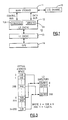
- FIG. 1 there is illustrated a block diagram of a prior art processor system 10 with a two-level cache.
- the processor CPU 14 is coupled to main storage (MS) 11 via an L1 cache 13 and L2 cache 12.
- the main storage 11 is also be coupled to an I/O device 15.
- the L2 cache includes arrays 12a and controls 12b.
- the L1 cache 13 will forward the request for the data to the L2 cache 12.
- the virtually addressed L2 cache 12 is searched for the desired data. If the data is found it is returned to the L1 cache 13 which sends it to the CPU 14. If the data does not reside in the L2 cache 12 it must be fetched from the main storage 11. Fetching the data from main storage 11 requires that the virtual address used to address the L2 12 cache be translated to a real address. The translation process typically involves one or more table look-ups before the data can be accessed from main storage.
- Fig. 2 shows the implementation of the invention on a 1 megabyte (1 MB) second level cache L2 12 that services a first level L1 cache 13 that interfaces to a processor 14 (CPU).
- the L2 cache 12 has a line size of 1 kilobyte (1 KB) and corresponding to each 1K block of data in the cache is a directory 20 entry containing among other things the most significant bits of the virtual address 21 (0:29) and the real 4 KB page addresses 23 (18:35) from which the data came from in main storage.
- the 1024 entries in directory 20 are organized in an array of 256 addresses or congruency classes by four sets (A, B, C, and D). Since the directory is addressed with bits 30 through 37 of the virtual address it is easy to determine which virtual addresses are placed or mapped into a particular row or congruency class of the directory.
- the virtual address of the first 1 KB block of the virtual address space is mapped into the first row or congruency class (class 0 or address 0).
- the virtual address of the second 1 KB block of the virtual address space is mapped into the second congruency class. And so on until 1 KB block number 255 of the virtual address space is mapped into congruency class 255.
- the mapping then wraps around with block 256 being mapped into congruency class 0. See Fig. 3.
- the L2 cache directory 20 is searched by first addressing it with bit numbers 30 through 37 of the 48 bit virtual address. The four sets for the addressed class are read and a comparison is done on a 30 bit virtual address stored for each set in the class along with the appropriate protection. bits. If a match exists then the desired data resides in the cache and a "hit" is signalled from the hit/miss logic 66. If a match cannot be made then a "miss" is signalled and the L2 cache 12 proceeds to request the data from the main storage 11.
- the L2 cache's 12 request for data from the main storage 11 requires that the virtual address used to address the L2 cache 12 be converted to a real address through an address translation algorithm.
- This algorithm first generates a request to main storage for a hash table entry followed by a request for a page table entry. The number of page frame table requests depends upon whether chaining of page table entries has occurred. Finally, a request is made to main storage 11 for the desired 1K line of data if the data exists in the main storage 11.
- a primary/secondary L2 cache directory searching method and apparatus would eliminate the request to main storage 11 for a hash table entry and page frame table entries when another 1K line from the same 4K page exists in the L2 cache 12.
- Each entry in the L2 cache 12 contains the real address of the 4K page from which it came from in the main storage 11. Therefore, if another line from the same page as the desired line could be located in the L2 cache 12 it would not be necessary to access the main storage 11 for the hash table and page frame table entries. This can be accomplished by placing entries for lines from the same 4K page of real storage in a specific relationship with respect to one another in the L2 cache directory 20.
- This relationship is provided, for example, by placing the 1K lines from the same 4K page in the sequential rows or congruency classes to be searched.
- the first 1K line of a given page is mapped into the first row 21a
- the second 1KB line of the page 0 is in second row 21b
- the third line of the page 0 is in the third row 21c
- the fourth line of the page 0 is in row 21d.
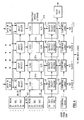
- Fig. 4 illustrates in more detail for a specific type of directory how the 1K byte lines from the same 4K page are placed in sets A of the directory.
- the bits 30-35 define a 4K byte page. There are 64 pages (0-63) in each set.
- the four 1K byte lines of a given page are simultaneously provided to output decode logic 41-44 and comparators 51-54. For example with bit numbers 30-35 all zeros the lines I/O, 2/0, 3/0 and 4/0 of page 0 are provided to the output decode 41-44 and -comparators 51-54.
- This placement of data in the directory is the same for the remaining sets (B, C and D) of the directory. From Fig.
- the virtual address bits stored in the cache will be compared against the virtual address bits (0:29) stored in the Directory Address Register (DAR) at comparators 51-54. If these two sets of bits are equal the compare out line(s) will be activated indicating the desired 1K byte line of data exists in the cache and/or another 1K line from the same 4K page of data is resident in the cache. This information will be sent to the hit/miss logic 66 shown in Fig. 2. If a "hit" occurs as to the primary class the "Hit Primary Class” line will be activated. A detailed description of the logic required to drive the "Hit Primary Class” line is shown in Fig. 6. From Fig. 6 it can be seen that if the H-it Class 0, 1, 2 or 3 lines are activated and the corresponding address bits (36 and 37) are activated the "Hit Primary Class” line will be activated.
- DAR Directory Address Register
- the "Hit Secondary Class” line will be activated in Fig. 2.
- the detailed 'logic required to activate the "Hit Secondary Class” line is shown in Fig. 6.
- the real address for the secondary line will be used to construct the address for the primary 1K line thus eliminating two or more accesses to the main storage 11 for a hash table and page frame table entries. The only access to main storage will be for the 1K line of desired data.
- the Direct Address Register (DAR) 31 and the Cache Address Register 33 (CAR) are loaded with the primary virtual address from the requesting lower level L1 cache.
- the virtual address bits (0:29) stored in the directory 20 for the four sets of the primary class and the 12 sets of the secondary class are compared at comparators 50-65 with the virtual address bits (0:29) in the DAR 31.
- the primary address in the CAR register 33 will then be updated to the secondary class address (i.e., bit numbers 36 and 37 updated in primary address). Bits 36 and 37 for the secondary class address are determined as shown in Figs. 7 and 8. The two bits 36 and 37 from the primary class will be saved in a two bit latch 68 for reuse. At time period 4 control bits associated with the CAR register 33 will cause its secondary class address to be loaded via leads 70 into the DAR 31 when the CAR 33 is granted priority. The two primary bits 36 and 37 saved in the above two bit latch will be reloaded into the CAR register 33. The CAR register 33 will now contain the virtual address of the primary class which will be used to load the data from Main Storage 11 into the L2 cache 12.
- the secondary class address in the DAR 31 will be used to address the directory 20.
- the Hit Primary Class and Hit Secondary Class lines will be inhibited.
- the appropriate real address (RA) bits (bits 18-35) from the directory will be placed in a Memory Address Register (MAR) 71.
- Bits (36-43) will be loaded from the CAR 33 into the MAR 71.
- This invention can be used in other cache configurations (associativity, line size, virtual address size).
- the invention can be used with any page size of main storage.
- the search for primary and secondary dine can be done sequentially rather than simultaneously. It is preferred to be simultaneous for improved cache performance.
Landscapes
- Engineering & Computer Science (AREA)
- Theoretical Computer Science (AREA)
- Physics & Mathematics (AREA)
- General Engineering & Computer Science (AREA)
- General Physics & Mathematics (AREA)
- Memory System Of A Hierarchy Structure (AREA)
Applications Claiming Priority (2)
| Application Number | Priority Date | Filing Date | Title |
|---|---|---|---|
| US391763 | 1982-06-24 | ||
| US07/391,763 US5077826A (en) | 1989-08-09 | 1989-08-09 | Cache performance in an information handling system employing page searching |
Publications (2)
| Publication Number | Publication Date |
|---|---|
| EP0412949A2 true EP0412949A2 (de) | 1991-02-13 |
| EP0412949A3 EP0412949A3 (en) | 1992-02-12 |
Family
ID=23547835
Family Applications (1)
| Application Number | Title | Priority Date | Filing Date |
|---|---|---|---|
| EP19900850262 Withdrawn EP0412949A3 (en) | 1989-08-09 | 1990-07-04 | Improved cache performance in an information handling system employing page searching |
Country Status (3)
| Country | Link |
|---|---|
| US (1) | US5077826A (de) |
| EP (1) | EP0412949A3 (de) |
| JP (1) | JPH0371355A (de) |
Cited By (2)
| Publication number | Priority date | Publication date | Assignee | Title |
|---|---|---|---|---|
| EP0560598A1 (de) * | 1992-03-13 | 1993-09-15 | STMicroelectronics Limited | Cache-Speicher |
| WO2000022531A1 (en) * | 1998-10-14 | 2000-04-20 | Telefonaktiebolaget Lm Ericsson (Publ) | System and method for improving memory access |
Families Citing this family (9)
| Publication number | Priority date | Publication date | Assignee | Title |
|---|---|---|---|---|
| JPH02205953A (ja) * | 1989-02-03 | 1990-08-15 | Nec Corp | アドレス変換装置 |
| US5249282A (en) * | 1990-11-21 | 1993-09-28 | Benchmarq Microelectronics, Inc. | Integrated cache memory system with primary and secondary cache memories |
| US5479630A (en) * | 1991-04-03 | 1995-12-26 | Silicon Graphics Inc. | Hybrid cache having physical-cache and virtual-cache characteristics and method for accessing same |
| US5446854A (en) * | 1993-10-20 | 1995-08-29 | Sun Microsystems, Inc. | Virtual memory computer apparatus and address translation mechanism employing hashing scheme and page frame descriptor that support multiple page sizes |
| US5721863A (en) * | 1996-01-29 | 1998-02-24 | International Business Machines Corporation | Method and structure for accessing semi-associative cache memory using multiple memories to store different components of the address |
| US5781922A (en) * | 1996-11-19 | 1998-07-14 | International Business Machines Corporation | Page boundary caches |
| US7257279B2 (en) * | 2004-09-20 | 2007-08-14 | 3M Innovative Properties Company | Systems and methods for biosensing and microresonator sensors for same |
| JP2008268386A (ja) * | 2007-04-18 | 2008-11-06 | Tokyo Electric Power Co Inc:The | 立体模型 |
| US11561906B2 (en) * | 2017-12-12 | 2023-01-24 | Advanced Micro Devices, Inc. | Rinsing cache lines from a common memory page to memory |
Family Cites Families (11)
| Publication number | Priority date | Publication date | Assignee | Title |
|---|---|---|---|---|
| US4441155A (en) * | 1981-11-23 | 1984-04-03 | International Business Machines Corporation | Page controlled cache directory addressing |
| JPS5898893A (ja) * | 1981-12-09 | 1983-06-11 | Toshiba Corp | 情報処理装置 |
| US4612612A (en) * | 1983-08-30 | 1986-09-16 | Amdahl Corporation | Virtually addressed cache |
| US4577293A (en) * | 1984-06-01 | 1986-03-18 | International Business Machines Corporation | Distributed, on-chip cache |
| US4985829A (en) * | 1984-07-31 | 1991-01-15 | Texas Instruments Incorporated | Cache hierarchy design for use in a memory management unit |
| US4991081A (en) * | 1984-10-31 | 1991-02-05 | Texas Instruments Incorporated | Cache memory addressable by both physical and virtual addresses |
| US4737909A (en) * | 1985-04-01 | 1988-04-12 | National Semiconductor Corp. | Cache memory address apparatus |
| US4785398A (en) * | 1985-12-19 | 1988-11-15 | Honeywell Bull Inc. | Virtual cache system using page level number generating CAM to access other memories for processing requests relating to a page |
| US4953073A (en) * | 1986-02-06 | 1990-08-28 | Mips Computer Systems, Inc. | Cup chip having tag comparator and address translation unit on chip and connected to off-chip cache and main memories |
| US4797814A (en) * | 1986-05-01 | 1989-01-10 | International Business Machines Corporation | Variable address mode cache |
| JPH07120312B2 (ja) * | 1987-10-07 | 1995-12-20 | 株式会社日立製作所 | バッファメモリ制御装置 |
-
1989
- 1989-08-09 US US07/391,763 patent/US5077826A/en not_active Expired - Fee Related
-
1990
- 1990-07-04 EP EP19900850262 patent/EP0412949A3/en not_active Withdrawn
- 1990-08-03 JP JP2205332A patent/JPH0371355A/ja active Granted
Cited By (3)
| Publication number | Priority date | Publication date | Assignee | Title |
|---|---|---|---|---|
| EP0560598A1 (de) * | 1992-03-13 | 1993-09-15 | STMicroelectronics Limited | Cache-Speicher |
| WO2000022531A1 (en) * | 1998-10-14 | 2000-04-20 | Telefonaktiebolaget Lm Ericsson (Publ) | System and method for improving memory access |
| US6279082B1 (en) | 1998-10-14 | 2001-08-21 | Telefonaktiebolaget Lm Ericsson (Publ) | System and method for efficient use of cache to improve access to memory of page type |
Also Published As
| Publication number | Publication date |
|---|---|
| US5077826A (en) | 1991-12-31 |
| JPH0529942B2 (de) | 1993-05-06 |
| EP0412949A3 (en) | 1992-02-12 |
| JPH0371355A (ja) | 1991-03-27 |
Similar Documents
| Publication | Publication Date | Title |
|---|---|---|
| US5628023A (en) | Virtual storage computer system having methods and apparatus for providing token-controlled access to protected pages of memory via a token-accessible view | |
| US4785398A (en) | Virtual cache system using page level number generating CAM to access other memories for processing requests relating to a page | |
| US5619671A (en) | Method and apparatus for providing token controlled access to protected pages of memory | |
| US5361340A (en) | Apparatus for maintaining consistency in a multiprocessor computer system using virtual caching | |
| US5329629A (en) | Apparatus and method for reading, writing, and refreshing memory with direct virtual or physical access | |
| US6205531B1 (en) | Method and apparatus for virtual address translation | |
| US6874077B2 (en) | Parallel distributed function translation lookaside buffer | |
| US3866183A (en) | Communications control apparatus for the use with a cache store | |
| US5060137A (en) | Explicit instructions for control of translation lookaside buffers | |
| US4241401A (en) | Virtual address translator utilizing interrupt level code | |
| US5241638A (en) | Dual cache memory | |
| US6073226A (en) | System and method for minimizing page tables in virtual memory systems | |
| JPH07200409A (ja) | 仮想アドレスを物理アドレスに変換する方法及び装置 | |
| CA2058259C (en) | Apparatus for increasing the number of hits in a translation lookaside buffer | |
| US5077826A (en) | Cache performance in an information handling system employing page searching | |
| US6009503A (en) | Cache memory indexing using virtual, primary and secondary color indexes | |
| JP2788836B2 (ja) | ディジタルコンピュータシステム | |
| EP0279189B1 (de) | Speicheranordnung | |
| EP0173909B1 (de) | LRU-Markiersteuerungsschaltung für look-aside Puffer | |
| EP0212129A2 (de) | Verfahren zur Aktualisierung der Informationen in einem Adressenübersetzungspufferspeicher | |
| US4710894A (en) | Access control system for storage having hardware area and software area | |
| EP0425771A2 (de) | Wirksamer Mechanismus zur Versorgung feinkörniger Speicherschutzbereiche | |
| JPS623354A (ja) | キヤツシユメモリ・アクセス方式 | |
| JP3068935B2 (ja) | エントリ置き換え制御方法 | |
| US6253301B1 (en) | Method and apparatus for a dedicated physically indexed copy of the data cache tag arrays |
Legal Events
| Date | Code | Title | Description |
|---|---|---|---|
| PUAI | Public reference made under article 153(3) epc to a published international application that has entered the european phase |
Free format text: ORIGINAL CODE: 0009012 |
|
| 17P | Request for examination filed |
Effective date: 19901213 |
|
| AK | Designated contracting states |
Kind code of ref document: A2 Designated state(s): DE FR GB |
|
| PUAL | Search report despatched |
Free format text: ORIGINAL CODE: 0009013 |
|
| AK | Designated contracting states |
Kind code of ref document: A3 Designated state(s): DE FR GB |
|
| 17Q | First examination report despatched |
Effective date: 19950112 |
|
| GRAG | Despatch of communication of intention to grant |
Free format text: ORIGINAL CODE: EPIDOS AGRA |
|
| STAA | Information on the status of an ep patent application or granted ep patent |
Free format text: STATUS: THE APPLICATION IS DEEMED TO BE WITHDRAWN |
|
| 18D | Application deemed to be withdrawn |
Effective date: 19970201 |