EP0413482A2 - Kontinuierliche Dünnschicht-Dynoden - Google Patents
Kontinuierliche Dünnschicht-Dynoden Download PDFInfo
- Publication number
- EP0413482A2 EP0413482A2 EP90308571A EP90308571A EP0413482A2 EP 0413482 A2 EP0413482 A2 EP 0413482A2 EP 90308571 A EP90308571 A EP 90308571A EP 90308571 A EP90308571 A EP 90308571A EP 0413482 A2 EP0413482 A2 EP 0413482A2
- Authority
- EP
- European Patent Office
- Prior art keywords
- substrate
- electron
- thin film
- emissive
- current carrying
- Prior art date
- Legal status (The legal status is an assumption and is not a legal conclusion. Google has not performed a legal analysis and makes no representation as to the accuracy of the status listed.)
- Granted
Links
Images


Classifications
-
- H—ELECTRICITY
- H01—ELECTRIC ELEMENTS
- H01J—ELECTRIC DISCHARGE TUBES OR DISCHARGE LAMPS
- H01J43/00—Secondary-emission tubes; Electron-multiplier tubes
- H01J43/04—Electron multipliers
- H01J43/06—Electrode arrangements
- H01J43/18—Electrode arrangements using essentially more than one dynode
- H01J43/24—Dynodes having potential gradient along their surfaces
- H01J43/246—Microchannel plates [MCP]
-
- H—ELECTRICITY
- H01—ELECTRIC ELEMENTS
- H01J—ELECTRIC DISCHARGE TUBES OR DISCHARGE LAMPS
- H01J49/00—Particle spectrometers or separator tubes
- H01J49/02—Details
- H01J49/025—Detectors specially adapted to particle spectrometers
-
- H—ELECTRICITY
- H01—ELECTRIC ELEMENTS
- H01J—ELECTRIC DISCHARGE TUBES OR DISCHARGE LAMPS
- H01J9/00—Apparatus or processes specially adapted for the manufacture, installation, removal, maintenance of electric discharge tubes, discharge lamps, or parts thereof; Recovery of material from discharge tubes or lamps
- H01J9/02—Manufacture of electrodes or electrode systems
- H01J9/12—Manufacture of electrodes or electrode systems of photo-emissive cathodes; of secondary-emission electrodes
-
- H—ELECTRICITY
- H01—ELECTRIC ELEMENTS
- H01J—ELECTRIC DISCHARGE TUBES OR DISCHARGE LAMPS
- H01J2201/00—Electrodes common to discharge tubes
- H01J2201/32—Secondary emission electrodes
-
- H—ELECTRICITY
- H01—ELECTRIC ELEMENTS
- H01J—ELECTRIC DISCHARGE TUBES OR DISCHARGE LAMPS
- H01J2201/00—Electrodes common to discharge tubes
- H01J2201/34—Photoemissive electrodes
- H01J2201/342—Cathodes
- H01J2201/3421—Composition of the emitting surface
- H01J2201/3423—Semiconductors, e.g. GaAs, NEA emitters
Definitions
- the invention relates to channel electron multipliers and microchannel plates.
- MCPs 20 are fabricated as areal arrays of millions of essentially independent channel electron multipliers 22 which operate simultaneously and in parallel.
- direct detection of charged particles and sufficiently energetic electromagnetic radiation can be achieved in two dimensions over large areas (up to several hundred cm2), with good resolution (channel spacing or pitch ⁇ 10 ⁇ m), at fast response times (output pulse widths ⁇ 300 ps), and with linear response over a broad range of input event levels (10 ⁇ 12-10 ⁇ 8A).
- an MCP between a suitable photocathode and fluorescent screen in an optical image tube (not shown), two-dimensional signals from the ultraviolet to the near-infrared spectral region can be intensified and displayed as a visible image.
- Typical values of ⁇ range from 30 to 80 for conventional CEMs and MCPs with channel diameters D on the scale of 1 mm and 10 ⁇ m, respectively.
- a CEM 10 is a single channel electron multiplier of macroscopic dimensions while MCP 20 is a wafer-thin array of microscopic electron multipliers with channel densities of 105-107/cm2.
- the channel wall 14 of CEM 10 or the wall 24 of the MCP 20 acts as a continuous dynode for electron multiplication and may be contrasted with the operation of photoemissive detectors using discrete dynodes (e.g., an ordinary photomultiplier tube).
- the continuous dynodes 14 and 24 must be sufficiently resistive to support a biasing electric field ( ⁇ ) 102-105 V/cm without drawing an excessive current. They must also be conductive enough such that a discharging current is available to replenish electrons emitted from the dynode 14,24 during an electron avalanche.
- a signal event 30 such as an electrically charged particle (Fig.
- Straight-channel multipliers are limited to electron gains of about 104 due to a phenomenon known as positive ion feedback. Near the output end of a channel multiplier and above some threshold gain, residual gas molecules within the channel or gasses adsorbed on the channel wall can become ionized by interaction with the electron avalanche. In contrast to the direction of travel for electrons with negative electrical charge, positive ions are accelerated toward the negatively-biased input end of the channel. Upon striking the channel wall, these ions cause the emission of electrons which are then multiplied geometrically by the process described above. Spurious and at times regenerative output pulses associated with ion feedback can thus severely degrade the signal-to-noise characteristics of the detector.
- An effective method for reducing ion feedback in channel multipliers is to curve the channel.
- Channel curvature restricts the distance that a positive ion can migrate toward the input end of a channel, and hence greatly reduces the amplitude of spurious output pulses.
- Single MCPs with straight channels typically provide electron gains of 103-104.
- Curved-channel MCPs can produce gains of 105-106 but are difficult and expensive to manufacture.
- Curved-channel CEMs can operate at gains in excess of 108.
- the near-surface region of the dynode must have an average value of ⁇ sufficiently greater than unity to support efficient multiplication of electrons impinging on a channel wall, as discussed above.
- RLSG dynodes During hydrogen reduction, other high-temperature processes including diffusion and evaporation of mobile chemical species in the lead silicate glass (e.g., alkali, alkaline earth, and lead atoms) also act to modify the chemistry and structure of RLSG dynodes. Compositional profiles through the near-surface region of glasses that are used in the manufacture of MCPs have indicated that RLSG dynodes have a two-layer structure.
- An exemplary RLSG dynode 50 shown in Fig. 3, comprises a superficial silica-rich and alkali-rich, but lead-poor dielectric emissive layer 52 about 2-20 nm in thickness (d) that produces adequate secondary emission (i.e., E P I ⁇ 30 eV) to achieve useful electron multiplication.
- a semiconductive lead-rich layer 54 Beneath this dielectric emissive layer 52 (or dynode surface), a semiconductive lead-rich layer 54 about 100-1000 nm in thickness (t) serves as an electronically conductive path for discharging the emissive layer 52.
- the GMD process also imposes important manufacturing constraints on the geometry, and hence on the performance and applications of RLSG MCPs in the following ways: channel diameters ⁇ 4 ⁇ m and channel pitches 6 ⁇ m in current practice limit temporal and spatial resolution; quasi-periodic arrays of channels within multifibre regions and gross discontinuities at adjacent multifibre boundaries greatly complicate the task of addressing or reading out individual or small blocks of channels; variations in channel diameter from area to area in an array are manifest as patterns with differential gain; and the largest size of a microchannel array is now limited to a linear dimension on the order of 10 cm.
- Our copending application (reference 90/3830/02) addresses these problems.
- the invention is directed to continuous dynodes formed by thin film processing techniques.
- a continuous dynode is disclosed in which at least one layer is formed by reacting a vapour in the presence of a substrate at a temperature and pressure sufficient to result in chemical vapour deposition kinetics dominated by interfacial processes between the vapour and the substrate.
- the surface of a substrate or surface of a thin film previously deposited on a substrate is subjected to a reactive atmosphere at a temperature and pressure sufficient to result in a reaction modifying the surface.
- a continuous dynode is formed in part by liquid phase deposition of a dynode material into the substrate from a supersaturated solution. The resulting devices exhibit conductive and emissive properties suitable for electron multiplication in CEM, MCP and MEM applications.
- current carrying (e.g. semiconductive) and dielectric thin films may be vapour deposited along the walls of capillary channels within suitable substrates to yield continuous dynodes which replicate the function of reduced lead silicate glass (RLSG) dynodes.
- Such devices may be comprised of thin film dynodes that are supported by dielectric or semiconductive substrates in the configuration of CEMs and MCPs.
- deposition of both a current carrying or semiconductive layer and an electron emissive layer would generally be necessary; however, appropriately semiconductive substrates would only require the deposition of an emissive layer.
- the dynode 60 comprises an emissive layer or film 62, a semiconductive layer or film 64 and a dielectric substrate 66.
- the dynode 60 is formed by depositing the semiconductive film such as silicon to a thickness t in the range of 10-1000 nm onto the surface 70 of the substrate 66 such as silica glass.
- a suitable dopant e.g., phosphorous
- SIPOS semi-insulating films
- deposition is achieved by a chemical vapour deposition (CVD) technique.
- CVD chemical vapour deposition
- the term CVD refers to the formation of thin films under conditions which are generally controlled by interfacial processes between gaseous reactants or reaction products and the substrate rather than by the transport of chemical species through the gas phase near the surface of the substrate.
- the emissive layer 62 may comprise a thin layer of SiO2, a native oxide about 2-5 nm in thickness d, overlying the silicon semiconductive layer 64, and be formed by exposure of the semiconductor surface 68 to ambient.
- the emissive layer 62 may be formed or grown to a thickness of 2-20 nm by oxidation or nitridation of the semiconductor surface 68 at elevated temperatures in the presence of reactive gases (e.g., O2 or NH3).
- d 2-20 nm upon the surface 68 of semiconductive layer 64 to form the basic two-layer structure of the thin film dynode 60.
- SiO2 if E P I ⁇ 40 eV and 6 ⁇ ⁇ E P /E P I , then 0.5 ⁇ ⁇ ⁇ 2.5 for 20 eV ⁇ E P ⁇ 100 eV; whereas for MgO, if E P I ⁇ 25 eV, then 0.8 ⁇ ⁇ ⁇ 4 for the same range of E P .
- semiconductive films with surfaces exhibiting negative electron affinity, and thus highly efficient secondary electron emission may also be formed by CVD methods (e.g., GaP:Cs-O, GaP:Ba-O, GaAs: Cs-O, InP:Cs-O and Si:Cs-O).
- CVD methods e.g., GaP:Cs-O, GaP:Ba-O, GaAs: Cs-O, InP:Cs-O and Si:Cs-O.
- the bias current for the dynode 72 could be carried throughout the bulk of the substrate 76. Also, as shown in the embodiment illustrated in Fig.
- the RLSG dynode 90 is comprised of a dielectric emissive layer 62 and an underlying semiconductive layer 54.
- This two-layer structure is mechanically supported by the lead silicate base glass 56 in channel geometries which are characteristic of CEMs or MCPs.
- the emissive layer 62 in contrast to prior RLSG dynodes (Fig. 3) is preferably formed by CVD of an appropriate material such as Si3N4, MgO, or the like.
- the semiconductive layer 54 may be formed by H2 reduction under conditions sufficient to promote formation of the semiconductive layer but minimize the formation of emissive layer 52, as in conventional RLSG dynodes (Fig. 3).
- Si3N4 acts as a hermetic seal to protect the underlying surfaces from environmental degradation thereby enhancing the product shelf life.
- Si3N4 and Al2O3 are also more resistant than SiO2 or SiO2-rich glasses to degradation under electron bombardment thereby extending the operational lifetime of the dynode.
- Electrodes 108 are formed on the exterior of the tube 102 and thin-film dynode 110 is formed on the interior of the tube as shown.
- the tube 102 is first subjected to a two-stage CVD process whereby the respective exterior and interior surfaces 114 and 112 are successively coated in a reactor (not shown) with a semiconductive layer 64 and emissive layer 62 which are shown in the enlargement.
- the exterior of the tube 102 is masked and stripped (e.g., by sandblasting or etching) to produce a nonconductive band 118 on the exterior wall 114.
- Metal electrodes 108 are thereafter applied by a suitable evaporation procedure.
- the semiconductive layer 64 and emissive layer 62 in the internal surface 112 functions as the continuous thin film dynode 110.
- CVD chemical vapour deposition
- suitable materials e.g. semiconductors or ceramics
- Temperature, pressure, and gaseous reactants are selected and balanced so that the physical structure and electrical and electron emissive properties of the dynodes so produced are appropriate for achieving the performance desired.
- Basic deposition reactions include pyrolysis, hydrolysis, disproportionation, oxidation, reduction, synthesis reactions and combinations of the above.
- LPCVD low pressure CVD
- LPCVD low pressure CVD
- LPCVD results in conformal thin-films usually having substantially uniform geometrical, electrical and electron emissive properties.
- the deposition reactions preferably occur heterogeneously at the substrate surface rather than homogeneously in the gas phase.
- Metal hydrides and halides as well as metal organics are common vapour precursors.
- the emissive portion of the dynodes of the present invention may be formed of SiO2, Al2O3, MgO, SnO2, BaO, Cs2O, Si3N4, Si x O y N z , C (Diamond), BN, and AlN; negative electron affinity emitters GaP:Cs-O, GaP:Ba-O, GaAs:Cs-O, InP:Cs-O, and Si:Cs-O.
- the current carrying portion of the dynodes according to the present invention may be formed of As-, B-, or P-doped Si, Ge (undoped), Si (undoped), SiO x (SIPOS), Si x N y , Al x Ga 1-x As, and SnO x .
- Precursors for such materials may be SiH4, PH3, GeH4, B2H6, AsH3, SnCl4, Ga(C2H5)3, Ga(CH3)3, Al(CH3)3, N2O, N2, and NH3.
- Tables I and II Selected representative examples of semiconductive and dielectric materials and their precursors which are of particular interest for fabrication of thin-film dynodes by CVD methods are given in Tables I and II, respectively.
- LPCVD thermally-activated CVD
- the resulting higher diffusivities of the reactant and product gasses cause the film growth rate to be controlled by kinetic processes at the gas-substrate interface (e.g., adsorption of reactants, surface migration of adatoms, chemical reaction, or desorption of reaction products) rather than by mass transport of the gasses through a stagnant boundary layer adjacent to the interface.
- T 300-1200°C
- conformal films can be heterogeneously deposited by LPCVD even over substantial contours because supply of an equal reactant flux to all locations on the substrate is not critical under surface reaction rate-limited conditions.
- Conformal coverage of films over complex topographies depends on rapid migration of adatoms prior to reaction.
- lower gas diffusivities promote mass transport-limited conditions where an equal reactant flux to all areas of the substrates is essential for film uniformity.
- LPCVD is thought to have a greater potential than APCVD for attaining the objective of depositing conformal conductive and emissive layers 64,62 with uniform thicknesses and properties within capillary substrate geometries to form thin-film dynodes for CEMs and MCPs.
- LPCVD can provide conformal films without the substrate 66 being in the line-of-sight of the vapour source, it is clearly superior to physical vapour deposition methods (e.g., evaporation and sputtering) for this application.
- Other noteworthy advantages of LPCVD include better compositional and structural control, lower deposition temperatures, fewer particulates due to homogeneous reactions, and lower processing costs.
- PCCVD photochemically-activated CVD
- the pressure may be raised to reduce gas transport and promote nonuniform deposition along the channel axis without departing from the invention.
- staged deposition may be achieved by producing one or more continuous, interconnected thin-film dynode elements, each being uniform over a substantial length.
- the deposition parameters may be held constant or varied gradually so that, respectively, a single compositionally uniform film is deposited which desirably exhibits both conductive and emissive properties, or the composition and properties of the film or films vary with thickness to achieve some desirable purpose.
- substrates for CEMs and MCPs should be comprised of materials that are readily formable into the geometries of such devices but also compatible with CVD processing methods.
- Contemplated deposition temperatures of 300-1200°C for LPCVD require a substrate to be sufficiently refractory so that it does not melt or distort during processing.
- the substrate should be chemically and mechanically suited to the overlying thin films such that deleterious interfacial reactions and stresses are avoided.
- the substrate should be made of a material with adequate chemical purity such that control over the deposition process and essential properties of the thin-film dynodes are not compromised by contamination effects.
- substrates with high thermal conductivity (k) would assist the dissipation of Joule heat.
- vapour deposition methods based on CVD can be used to fabricate continuous thin-film dynodes with electrical and electron emissive properties that are comparable to those obtained with conventional RLSG dynodes. Because of this, more efficient manufacturing procedures for CEMs and MCPs are available, including improvements in RLSG configurations. Further, it is expected that significant improvements in the performance of CEMs and MCPs made in accordance with the teachings of the present invention can be achieved by capitalizing on the ability to tailor the materials and structure of thin-film dynodes.
- the advantages which may be achievable include better multiplication statistics and operation at a lower external bias potential V B by deposition of an emissive layer 62 with higher secondary electron yield ⁇ than conventional RLSG dynodes (e.g., MgO or negative electron affinity emitters such as GaP:Cs-O). Better gain stability and longer operational lifetimes (e.g., 100 C/cm2 of extracted charge) are achievable by use of an emissive layer 62 such as Si3N4 or Al2O3which exhibits low susceptibility to outgassing or degradation by electron irradiation. Improved noise characteristics and extended dynamic range result from choice of high-purity materials for dynodes and substrates which are free of radioactive impurities, a major source of background noise.
- an emissive layer 62 with higher secondary electron yield ⁇ than conventional RLSG dynodes e.g., MgO or negative electron affinity emitters such as GaP:Cs-O.
- Thin-film processing according to the present invention includes the surface treatment of deposited or bulk semiconductor materials to achieve desirable electron emissivity.
- a bulk semiconductor 76 such as silicon may be treated in a similar manner to produce an emissive surface.
- dielectric films such as SiO2 may be formed by liquid phase deposition (LPD) to form the emissive layer 62 or the isolation layer 84 in the embodiments of Figs. 4-7.
- LPD liquid phase deposition
- SiO2 films can be deposited at 25-50°C onto the interior surfaces of macroscopic or microscopic capillary channels of CEMs or MCPs from a supersaturated aqueous solution of H2SiF6 and SiO2 with a small addition of H3BO3.
- LPD liquid phase deposition
- the substrates were first cleaned by a standard procedure and then placed inside a hot-wall, horizontal-tube, LPCVD reactor for deposition of silicon thin films.
- amorphous P-doped silicon films were formed on another set of substrates by reaction of PH3 and SiH4 in a reactant ratio of PH3/SiH4 5 x 10 ⁇ 4 under otherwise similar conditions.
- Semiconductive films 64 of thickness t ⁇ 300 nm were thus deposited on surfaces 112,114 of capillary substrates 102 (Fig. 8) at a rate of 1-10 nm/min.
- the capillary substrates were allowed to cool in the reactor and then were assembled into CEMs 100 as follows. Electrical continuity along the outer surface 114 of the capillary tubes was broken by removing the silicon deposit within a narrow band 118 around this outer surface (Fig. 8). Nichrome electrodes 108 were then vacuum-evaporated onto the ends of each tube without coating the non-conductive band between them. Each CEM was completed by attaching electrical leads to both electrodes.
- Fused quartz plates 25 x 60 x 1 mm similar to the plates 142 that are illustrated in Fig. 10, were used as substrates to form thin-film dynodes for a MEM 140.
- Amorphous P-doped silicon films with t ⁇ 300 nm and R S ⁇ 108 ⁇ /sq were formed on the planar substrates 142 using methods and conditions similar to those described in Example I for the CEMs.
- the MEM was assembled as follows. The silicon deposit was removed from one flat surface 151. A pattern of nichrome electrodes was then deposited through a mask (not shown) onto the other side of each plate 142 with the silicon deposit 148. A set of two plates 142 with closely matched R S were used as field and dynode strips to construct the MEM 140.
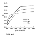
- Pulse counting measurements on the MEM 140 yielded the pulse height distribution given in Fig. 14.
- the structure of the thin-film dynodes in the above described CEMs 100 and MEM 140 of Examples I and II approximates the embodiment depicted in Fig. 4.
- the feasibility of such thin film dynodes to support practical levels of electron multiplication has clearly been established by the foregoing Examples. Further, the ability to tailor the current transfer characteristics of an electron multiplier by adjusting the current-carrying properties of a thin-film dynode has been demonstrated.
Landscapes
- Chemical & Material Sciences (AREA)
- Analytical Chemistry (AREA)
- Engineering & Computer Science (AREA)
- Manufacturing & Machinery (AREA)
- Electron Tubes For Measurement (AREA)
- Formation Of Insulating Films (AREA)
Applications Claiming Priority (2)
| Application Number | Priority Date | Filing Date | Title |
|---|---|---|---|
| US39558889A | 1989-08-18 | 1989-08-18 | |
| US395588 | 1989-08-18 |
Publications (3)
| Publication Number | Publication Date |
|---|---|
| EP0413482A2 true EP0413482A2 (de) | 1991-02-20 |
| EP0413482A3 EP0413482A3 (en) | 1991-07-10 |
| EP0413482B1 EP0413482B1 (de) | 1997-03-12 |
Family
ID=23563665
Family Applications (1)
| Application Number | Title | Priority Date | Filing Date |
|---|---|---|---|
| EP90308571A Expired - Lifetime EP0413482B1 (de) | 1989-08-18 | 1990-08-03 | Kontinuierliche Dünnschicht-Dynoden |
Country Status (4)
| Country | Link |
|---|---|
| US (2) | US5378960A (de) |
| EP (1) | EP0413482B1 (de) |
| JP (1) | JP3113902B2 (de) |
| DE (1) | DE69030145T2 (de) |
Cited By (7)
| Publication number | Priority date | Publication date | Assignee | Title |
|---|---|---|---|---|
| GB2293042A (en) * | 1994-09-03 | 1996-03-13 | Ibm | Electron multiplier, e.g. for a field emission display |
| EP0908917A3 (de) * | 1997-10-10 | 2000-03-22 | Burle Technologies, Inc. | Sekundäremissionsbechichtung für Vervielfacherröhren |
| EP1592041A2 (de) * | 2004-04-29 | 2005-11-02 | Burle Technologies, Inc. | Detektor für ein bipolares Laufzeitmassenspektrometer |
| GB2423629A (en) * | 2005-02-03 | 2006-08-30 | Bruker Daltonik Gmbh | Multichannel transport of ions into a mass spectrometer vacuum system |
| US7270813B2 (en) | 2002-10-08 | 2007-09-18 | Osteotech, Inc. | Coupling agents for orthopedic biomaterials |
| US7495211B2 (en) | 2004-12-22 | 2009-02-24 | Bruker Daltonik Gmbh | Measuring methods for ion cyclotron resonance mass spectrometers |
| EP1670030B1 (de) * | 2003-09-10 | 2017-07-19 | Hamamatsu Photonics K.K. | Elektronenröhre |
Families Citing this family (53)
| Publication number | Priority date | Publication date | Assignee | Title |
|---|---|---|---|---|
| US5440115A (en) * | 1994-04-05 | 1995-08-08 | Galileo Electro-Optics Corporation | Zener diode biased electron multiplier with stable gain characteristic |
| US5569355A (en) * | 1995-01-11 | 1996-10-29 | Center For Advanced Fiberoptic Applications | Method for fabrication of microchannel electron multipliers |
| DE19506165A1 (de) * | 1995-02-22 | 1996-05-23 | Siemens Ag | Elektronenvervielfacher und Verfahren zu dessen Herstellung |
| US6522061B1 (en) | 1995-04-04 | 2003-02-18 | Harry F. Lockwood | Field emission device with microchannel gain element |
| US5729244A (en) * | 1995-04-04 | 1998-03-17 | Lockwood; Harry F. | Field emission device with microchannel gain element |
| US5680008A (en) * | 1995-04-05 | 1997-10-21 | Advanced Technology Materials, Inc. | Compact low-noise dynodes incorporating semiconductor secondary electron emitting materials |
| US5618217A (en) * | 1995-07-25 | 1997-04-08 | Center For Advanced Fiberoptic Applications | Method for fabrication of discrete dynode electron multipliers |
| KR19980701858A (ko) * | 1995-12-06 | 1998-06-25 | 요트. 게. 아. 롤페즈 | 유리 기판 제조 방법 및 전자 디스플레이용 유리 기판 |
| US6045677A (en) * | 1996-02-28 | 2000-04-04 | Nanosciences Corporation | Microporous microchannel plates and method of manufacturing same |
| TW337592B (en) * | 1997-04-03 | 1998-08-01 | Nat Science Council | Process of depositing silicon dioxide on a group III-V semiconductor substrate by ammoniation treatment |
| AU7933398A (en) * | 1998-06-25 | 2000-01-10 | Hamamatsu Photonics K.K. | Photocathode |
| US6326654B1 (en) | 1999-02-05 | 2001-12-04 | The United States Of America As Represented By The Secretary Of The Air Force | Hybrid ultraviolet detector |
| US6396049B1 (en) * | 2000-01-31 | 2002-05-28 | Northrop Grumman Corporation | Microchannel plate having an enhanced coating |
| KR100496281B1 (ko) * | 2000-02-07 | 2005-06-17 | 삼성에스디아이 주식회사 | 2차 전자 증폭 구조체를 채용한 마이크로 채널 플레이트및 이를 이용한 전계 방출 소자 |
| US6828729B1 (en) * | 2000-03-16 | 2004-12-07 | Burle Technologies, Inc. | Bipolar time-of-flight detector, cartridge and detection method |
| US6642637B1 (en) | 2000-03-28 | 2003-11-04 | Applied Materials, Inc. | Parallel plate electron multiplier |
| JP2001351509A (ja) * | 2000-06-08 | 2001-12-21 | Hamamatsu Photonics Kk | マイクロチャネルプレート |
| US6642526B2 (en) * | 2001-06-25 | 2003-11-04 | Ionfinity Llc | Field ionizing elements and applications thereof |
| KR100403221B1 (ko) * | 2001-07-23 | 2003-10-23 | 한국수력원자력 주식회사 | 방사성 전자 방출 마이크로채널 판 |
| WO2003038086A1 (en) * | 2001-10-31 | 2003-05-08 | Ionfinity Llc | Soft ionization device and applications thereof |
| KR100873634B1 (ko) * | 2002-02-20 | 2008-12-12 | 삼성전자주식회사 | 탄소나노튜브를 포함하는 전자증폭기 및 그 제조방법 |
| US6828714B2 (en) * | 2002-05-03 | 2004-12-07 | Nova Scientific, Inc. | Electron multipliers and radiation detectors |
| US7154086B2 (en) * | 2003-03-19 | 2006-12-26 | Burle Technologies, Inc. | Conductive tube for use as a reflectron lens |
| GB0512001D0 (en) * | 2005-06-13 | 2005-07-20 | Council Cent Lab Res Councils | Electron amplifier device |
| US7408142B2 (en) | 2005-09-16 | 2008-08-05 | Arradiance, Inc. | Microchannel amplifier with tailored pore resistance |
| US20080073516A1 (en) * | 2006-03-10 | 2008-03-27 | Laprade Bruce N | Resistive glass structures used to shape electric fields in analytical instruments |
| US7855493B2 (en) * | 2008-02-27 | 2010-12-21 | Arradiance, Inc. | Microchannel plate devices with multiple emissive layers |
| US8052884B2 (en) | 2008-02-27 | 2011-11-08 | Arradiance, Inc. | Method of fabricating microchannel plate devices with multiple emissive layers |
| EP2274762B1 (de) * | 2008-04-10 | 2018-06-06 | Arradiance, LLC | Bildverstärkervorrichtung |
| US8237129B2 (en) * | 2008-06-20 | 2012-08-07 | Arradiance, Inc. | Microchannel plate devices with tunable resistive films |
| US8227965B2 (en) * | 2008-06-20 | 2012-07-24 | Arradiance, Inc. | Microchannel plate devices with tunable resistive films |
| US7759138B2 (en) * | 2008-09-20 | 2010-07-20 | Arradiance, Inc. | Silicon microchannel plate devices with smooth pores and precise dimensions |
| CA2684811C (en) * | 2009-11-06 | 2017-05-23 | Bubble Technology Industries Inc. | Microstructure photomultiplier assembly |
| US9105379B2 (en) | 2011-01-21 | 2015-08-11 | Uchicago Argonne, Llc | Tunable resistance coatings |
| US8969823B2 (en) | 2011-01-21 | 2015-03-03 | Uchicago Argonne, Llc | Microchannel plate detector and methods for their fabrication |
| US8921799B2 (en) | 2011-01-21 | 2014-12-30 | Uchicago Argonne, Llc | Tunable resistance coatings |
| JP6226865B2 (ja) * | 2012-05-18 | 2017-11-08 | 浜松ホトニクス株式会社 | マイクロチャネルプレートの製造方法 |
| JP5981820B2 (ja) * | 2012-09-25 | 2016-08-31 | 浜松ホトニクス株式会社 | マイクロチャンネルプレート、マイクロチャンネルプレートの製造方法、及びイメージインテンシファイア |
| US11326255B2 (en) * | 2013-02-07 | 2022-05-10 | Uchicago Argonne, Llc | ALD reactor for coating porous substrates |
| US9425030B2 (en) | 2013-06-06 | 2016-08-23 | Burle Technologies, Inc. | Electrostatic suppression of ion feedback in a microchannel plate photomultiplier |
| JP6407767B2 (ja) * | 2015-03-03 | 2018-10-17 | 浜松ホトニクス株式会社 | 電子増倍体の製造方法、光電子増倍管、及び光電子増倍器 |
| JP6496217B2 (ja) * | 2015-09-04 | 2019-04-03 | 浜松ホトニクス株式会社 | マイクロチャンネルプレート及び電子増倍体 |
| JP6734738B2 (ja) * | 2016-08-31 | 2020-08-05 | 浜松ホトニクス株式会社 | 電子増倍体、及び、光電子増倍管 |
| JP6738244B2 (ja) * | 2016-08-31 | 2020-08-12 | 浜松ホトニクス株式会社 | 電子増倍体の製造方法及び電子増倍体 |
| JP6983956B2 (ja) * | 2016-08-31 | 2021-12-17 | 浜松ホトニクス株式会社 | 電子増倍体 |
| JP6395906B1 (ja) * | 2017-06-30 | 2018-09-26 | 浜松ホトニクス株式会社 | 電子増倍体 |
| KR20200094130A (ko) * | 2017-10-09 | 2020-08-06 | 아답타스 솔루션즈 피티와이 엘티디 | 다이노드 전자 방출 표면 위의 오염물 부착을 억제하는 방법 및 장치 |
| JP6899868B2 (ja) | 2018-07-02 | 2021-07-07 | フォトニス・サイエンティフィック・インコーポレイテッドPhotonis Scientific, Inc. | 流れ及び1投与量の変動を減少させる方法によるアスペクト比が大きい物体への異なるコーティング |
| US11111578B1 (en) | 2020-02-13 | 2021-09-07 | Uchicago Argonne, Llc | Atomic layer deposition of fluoride thin films |
| IL310540A (en) * | 2021-08-16 | 2024-03-01 | Sionyx Llc | Microchannel plate image intensifiers and methods of producing the same |
| US12065738B2 (en) | 2021-10-22 | 2024-08-20 | Uchicago Argonne, Llc | Method of making thin films of sodium fluorides and their derivatives by ALD |
| US11901169B2 (en) | 2022-02-14 | 2024-02-13 | Uchicago Argonne, Llc | Barrier coatings |
| CN120183982B (zh) * | 2025-05-21 | 2026-02-27 | 中国建筑材料科学研究总院有限公司 | 一种梯度直径微通道板及其制备方法和应用 |
Family Cites Families (32)
| Publication number | Priority date | Publication date | Assignee | Title |
|---|---|---|---|---|
| US2841729A (en) * | 1955-09-01 | 1958-07-01 | Bendix Aviat Corp | Magnetic electron multiplier |
| US3244922A (en) * | 1962-11-05 | 1966-04-05 | Itt | Electron multiplier having undulated passage with semiconductive secondary emissive coating |
| US4073989A (en) * | 1964-01-17 | 1978-02-14 | Horizons Incorporated | Continuous channel electron beam multiplier |
| US4095132A (en) * | 1964-09-11 | 1978-06-13 | Galileo Electro-Optics Corp. | Electron multiplier |
| US3488509A (en) * | 1964-12-07 | 1970-01-06 | Bendix Corp | Particle acceleration having low electron gain |
| US3675063A (en) * | 1970-01-02 | 1972-07-04 | Stanford Research Inst | High current continuous dynode electron multiplier |
| US3911167A (en) * | 1970-05-01 | 1975-10-07 | Texas Instruments Inc | Electron multiplier and method of making same |
| US4095136A (en) * | 1971-10-28 | 1978-06-13 | Varian Associates, Inc. | Image tube employing a microchannel electron multiplier |
| USRE31847E (en) * | 1973-01-02 | 1985-03-12 | Eastman Kodak Company | Apparatus and method for producing images corresponding to patterns of high energy radiation |
| JPS5443869B2 (de) * | 1973-03-05 | 1979-12-22 | ||
| IL42668A (en) * | 1973-07-05 | 1976-02-29 | Seidman A | Channel electron multipliers |
| US4352985A (en) * | 1974-01-08 | 1982-10-05 | Martin Frederick W | Scanning ion microscope |
| US3959038A (en) * | 1975-04-30 | 1976-05-25 | The United States Of America As Represented By The Secretary Of The Army | Electron emitter and method of fabrication |
| US4015159A (en) * | 1975-09-15 | 1977-03-29 | Bell Telephone Laboratories, Incorporated | Semiconductor integrated circuit transistor detector array for channel electron multiplier |
| US4099079A (en) * | 1975-10-30 | 1978-07-04 | U.S. Philips Corporation | Secondary-emissive layers |
| JPS6013257B2 (ja) * | 1976-02-20 | 1985-04-05 | 松下電器産業株式会社 | 二次電子増倍体およびその製造方法 |
| US4051403A (en) * | 1976-08-10 | 1977-09-27 | The United States Of America As Represented By The Secretary Of The Army | Channel plate multiplier having higher secondary emission coefficient near input |
| US4236073A (en) * | 1977-05-27 | 1980-11-25 | Martin Frederick W | Scanning ion microscope |
| CA1121858A (en) * | 1978-10-13 | 1982-04-13 | Jean-Denis Carette | Electron multiplier device |
| JPS6042573B2 (ja) * | 1979-01-24 | 1985-09-24 | 浜松ホトニクス株式会社 | 二次電子増倍電極 |
| FR2507386A1 (fr) * | 1981-06-03 | 1982-12-10 | Labo Electronique Physique | Dispositif semi-conducteur, emetteur d'electrons, dont la couche active possede un gradient de dopage |
| US4454422A (en) * | 1982-01-27 | 1984-06-12 | Siemens Gammasonics, Inc. | Radiation detector assembly for generating a two-dimensional image |
| DE3332995A1 (de) * | 1983-07-14 | 1985-01-24 | Nippon Sheet Glass Co. Ltd., Osaka | Verfahren zum herstellen einer siliciumdioxidbeschichtung |
| US4577133A (en) * | 1983-10-27 | 1986-03-18 | Wilson Ronald E | Flat panel display and method of manufacture |
| DE3408848C2 (de) * | 1984-03-10 | 1987-04-16 | Kernforschungszentrum Karlsruhe Gmbh, 7500 Karlsruhe | Verfahren zur Herstellung von Vielkanalplatten |
| US4558144A (en) * | 1984-10-19 | 1985-12-10 | Corning Glass Works | Volatile metal complexes |
| FR2586508B1 (fr) * | 1985-08-23 | 1988-08-26 | Thomson Csf | Scintillateur d'ecran d'entree de tube intensificateur d'images radiologiques et procede de fabrication d'un tel scintillateur |
| US4825118A (en) * | 1985-09-06 | 1989-04-25 | Hamamatsu Photonics Kabushiki Kaisha | Electron multiplier device |
| GB2180986B (en) * | 1985-09-25 | 1989-08-23 | English Electric Valve Co Ltd | Image intensifiers |
| US4780395A (en) * | 1986-01-25 | 1988-10-25 | Kabushiki Kaisha Toshiba | Microchannel plate and a method for manufacturing the same |
| US4757229A (en) * | 1986-11-19 | 1988-07-12 | K And M Electronics, Inc. | Channel electron multiplier |
| US4800263A (en) * | 1987-02-17 | 1989-01-24 | Optron Systems, Inc. | Completely cross-talk free high spatial resolution 2D bistable light modulation |
-
1990
- 1990-08-03 DE DE69030145T patent/DE69030145T2/de not_active Expired - Fee Related
- 1990-08-03 EP EP90308571A patent/EP0413482B1/de not_active Expired - Lifetime
- 1990-08-17 JP JP02216929A patent/JP3113902B2/ja not_active Expired - Lifetime
-
1993
- 1993-07-12 US US08/089,771 patent/US5378960A/en not_active Expired - Lifetime
-
1994
- 1994-12-28 US US08/365,242 patent/US5726076A/en not_active Expired - Lifetime
Cited By (8)
| Publication number | Priority date | Publication date | Assignee | Title |
|---|---|---|---|---|
| GB2293042A (en) * | 1994-09-03 | 1996-03-13 | Ibm | Electron multiplier, e.g. for a field emission display |
| EP0908917A3 (de) * | 1997-10-10 | 2000-03-22 | Burle Technologies, Inc. | Sekundäremissionsbechichtung für Vervielfacherröhren |
| US7270813B2 (en) | 2002-10-08 | 2007-09-18 | Osteotech, Inc. | Coupling agents for orthopedic biomaterials |
| EP1670030B1 (de) * | 2003-09-10 | 2017-07-19 | Hamamatsu Photonics K.K. | Elektronenröhre |
| EP1592041A2 (de) * | 2004-04-29 | 2005-11-02 | Burle Technologies, Inc. | Detektor für ein bipolares Laufzeitmassenspektrometer |
| US7495211B2 (en) | 2004-12-22 | 2009-02-24 | Bruker Daltonik Gmbh | Measuring methods for ion cyclotron resonance mass spectrometers |
| GB2423629A (en) * | 2005-02-03 | 2006-08-30 | Bruker Daltonik Gmbh | Multichannel transport of ions into a mass spectrometer vacuum system |
| GB2423629B (en) * | 2005-02-03 | 2009-09-23 | Bruker Daltonik Gmbh | Transport of ions into a vacuum |
Also Published As
| Publication number | Publication date |
|---|---|
| JPH03116626A (ja) | 1991-05-17 |
| US5726076A (en) | 1998-03-10 |
| DE69030145T2 (de) | 1997-07-10 |
| EP0413482A3 (en) | 1991-07-10 |
| DE69030145D1 (de) | 1997-04-17 |
| US5378960A (en) | 1995-01-03 |
| EP0413482B1 (de) | 1997-03-12 |
| JP3113902B2 (ja) | 2000-12-04 |
Similar Documents
| Publication | Publication Date | Title |
|---|---|---|
| EP0413482B1 (de) | Kontinuierliche Dünnschicht-Dynoden | |
| JP6475916B2 (ja) | 調整可能な抵抗膜を有するマイクロチャネルプレートデバイス | |
| US8052884B2 (en) | Method of fabricating microchannel plate devices with multiple emissive layers | |
| US5565729A (en) | Microchannel plate technology | |
| EP0413481B1 (de) | Mikrokanal-Elektronenvervielfacher und Herstellungsverfahren | |
| US20120273689A1 (en) | Microchannel Plate Devices With Tunable Resistive Films | |
| CA1122256A (en) | Bonded cathode and electrode structure with layered insulation, and method of manufacture | |
| US7759138B2 (en) | Silicon microchannel plate devices with smooth pores and precise dimensions | |
| Beetz et al. | Silicon-micromachined microchannel plates | |
| US6384519B1 (en) | Micro-dynode integrated electron multiplier | |
| US5598056A (en) | Multilayer pillar structure for improved field emission devices | |
| US5568013A (en) | Micro-fabricated electron multipliers | |
| WO1998019341A9 (en) | Microdynode integrated electron multiplier | |
| US3900305A (en) | Method of forming conductive layer on oxide-containing surfaces | |
| Horton et al. | Characteristics and applications of advanced technology microchannel plates | |
| US20050136178A1 (en) | Method and apparatus for producing microchannel plate using corrugated mold | |
| EP0908917B1 (de) | Sekundäremissionsbechichtung für Vervielfacherröhren | |
| Winn | Large photocathode detectors for large calorimetry | |
| Tasker et al. | Thin-film amorphous silicon dynodes for electron multiplication | |
| JPH11120899A (ja) | 二次電子放出装置及びそれを用いた電子管 | |
| Winn | High gain photodetectors formed by nano/micromachining and nanofabrication |
Legal Events
| Date | Code | Title | Description |
|---|---|---|---|
| PUAI | Public reference made under article 153(3) epc to a published international application that has entered the european phase |
Free format text: ORIGINAL CODE: 0009012 |
|
| AK | Designated contracting states |
Kind code of ref document: A2 Designated state(s): DE FR GB NL |
|
| PUAL | Search report despatched |
Free format text: ORIGINAL CODE: 0009013 |
|
| AK | Designated contracting states |
Kind code of ref document: A3 Designated state(s): DE FR GB NL |
|
| 17P | Request for examination filed |
Effective date: 19920109 |
|
| 17Q | First examination report despatched |
Effective date: 19940126 |
|
| GRAG | Despatch of communication of intention to grant |
Free format text: ORIGINAL CODE: EPIDOS AGRA |
|
| GRAH | Despatch of communication of intention to grant a patent |
Free format text: ORIGINAL CODE: EPIDOS IGRA |
|
| GRAH | Despatch of communication of intention to grant a patent |
Free format text: ORIGINAL CODE: EPIDOS IGRA |
|
| GRAA | (expected) grant |
Free format text: ORIGINAL CODE: 0009210 |
|
| AK | Designated contracting states |
Kind code of ref document: B1 Designated state(s): DE FR GB NL |
|
| REF | Corresponds to: |
Ref document number: 69030145 Country of ref document: DE Date of ref document: 19970417 |
|
| ET | Fr: translation filed | ||
| PLBE | No opposition filed within time limit |
Free format text: ORIGINAL CODE: 0009261 |
|
| STAA | Information on the status of an ep patent application or granted ep patent |
Free format text: STATUS: NO OPPOSITION FILED WITHIN TIME LIMIT |
|
| PGFP | Annual fee paid to national office [announced via postgrant information from national office to epo] |
Ref country code: GB Payment date: 19980122 Year of fee payment: 8 |
|
| PGFP | Annual fee paid to national office [announced via postgrant information from national office to epo] |
Ref country code: FR Payment date: 19980128 Year of fee payment: 8 |
|
| PGFP | Annual fee paid to national office [announced via postgrant information from national office to epo] |
Ref country code: NL Payment date: 19980130 Year of fee payment: 8 |
|
| PGFP | Annual fee paid to national office [announced via postgrant information from national office to epo] |
Ref country code: DE Payment date: 19980202 Year of fee payment: 8 |
|
| 26N | No opposition filed | ||
| PG25 | Lapsed in a contracting state [announced via postgrant information from national office to epo] |
Ref country code: GB Free format text: LAPSE BECAUSE OF NON-PAYMENT OF DUE FEES Effective date: 19980803 |
|
| PG25 | Lapsed in a contracting state [announced via postgrant information from national office to epo] |
Ref country code: NL Free format text: LAPSE BECAUSE OF NON-PAYMENT OF DUE FEES Effective date: 19990301 |
|
| GBPC | Gb: european patent ceased through non-payment of renewal fee |
Effective date: 19980803 |
|
| PG25 | Lapsed in a contracting state [announced via postgrant information from national office to epo] |
Ref country code: FR Free format text: LAPSE BECAUSE OF NON-PAYMENT OF DUE FEES Effective date: 19990430 |
|
| NLV4 | Nl: lapsed or anulled due to non-payment of the annual fee |
Effective date: 19990301 |
|
| PG25 | Lapsed in a contracting state [announced via postgrant information from national office to epo] |
Ref country code: DE Free format text: LAPSE BECAUSE OF NON-PAYMENT OF DUE FEES Effective date: 19990601 |
|
| REG | Reference to a national code |
Ref country code: FR Ref legal event code: ST |