EP0413962A1 - Bilderzeugender Schirm für die Elektrophorese und Vorrichtung zur Bildwiedergabe - Google Patents
Bilderzeugender Schirm für die Elektrophorese und Vorrichtung zur Bildwiedergabe Download PDFInfo
- Publication number
- EP0413962A1 EP0413962A1 EP90113742A EP90113742A EP0413962A1 EP 0413962 A1 EP0413962 A1 EP 0413962A1 EP 90113742 A EP90113742 A EP 90113742A EP 90113742 A EP90113742 A EP 90113742A EP 0413962 A1 EP0413962 A1 EP 0413962A1
- Authority
- EP
- European Patent Office
- Prior art keywords
- emission
- pattern
- electron trapping
- trapping material
- optical energy
- Prior art date
- Legal status (The legal status is an assumption and is not a legal conclusion. Google has not performed a legal analysis and makes no representation as to the accuracy of the status listed.)
- Granted
Links
Images


Classifications
-
- G—PHYSICS
- G11—INFORMATION STORAGE
- G11B—INFORMATION STORAGE BASED ON RELATIVE MOVEMENT BETWEEN RECORD CARRIER AND TRANSDUCER
- G11B7/00—Recording or reproducing by optical means, e.g. recording using a thermal beam of optical radiation by modifying optical properties or the physical structure, reproducing using an optical beam at lower power by sensing optical properties; Record carriers therefor
- G11B7/004—Recording, reproducing or erasing methods; Read, write or erase circuits therefor
- G11B7/0045—Recording
- G11B7/00453—Recording involving spectral or photochemical hole burning
-
- C—CHEMISTRY; METALLURGY
- C09—DYES; PAINTS; POLISHES; NATURAL RESINS; ADHESIVES; COMPOSITIONS NOT OTHERWISE PROVIDED FOR; APPLICATIONS OF MATERIALS NOT OTHERWISE PROVIDED FOR
- C09K—MATERIALS FOR MISCELLANEOUS APPLICATIONS, NOT PROVIDED FOR ELSEWHERE
- C09K11/00—Luminescent materials, e.g. electroluminescent or chemiluminescent
- C09K11/08—Luminescent materials, e.g. electroluminescent or chemiluminescent containing inorganic luminescent materials
- C09K11/77—Luminescent materials, e.g. electroluminescent or chemiluminescent containing inorganic luminescent materials containing rare earth metals
- C09K11/7766—Luminescent materials, e.g. electroluminescent or chemiluminescent containing inorganic luminescent materials containing rare earth metals containing two or more rare earth metals
- C09K11/7767—Chalcogenides
- C09K11/7768—Chalcogenides with alkaline earth metals
-
- C—CHEMISTRY; METALLURGY
- C09—DYES; PAINTS; POLISHES; NATURAL RESINS; ADHESIVES; COMPOSITIONS NOT OTHERWISE PROVIDED FOR; APPLICATIONS OF MATERIALS NOT OTHERWISE PROVIDED FOR
- C09K—MATERIALS FOR MISCELLANEOUS APPLICATIONS, NOT PROVIDED FOR ELSEWHERE
- C09K11/00—Luminescent materials, e.g. electroluminescent or chemiluminescent
- C09K11/08—Luminescent materials, e.g. electroluminescent or chemiluminescent containing inorganic luminescent materials
- C09K11/77—Luminescent materials, e.g. electroluminescent or chemiluminescent containing inorganic luminescent materials containing rare earth metals
- C09K11/7783—Luminescent materials, e.g. electroluminescent or chemiluminescent containing inorganic luminescent materials containing rare earth metals containing two or more rare earth metals one of which being europium
- C09K11/7784—Chalcogenides
- C09K11/7786—Chalcogenides with alkaline earth metals
-
- C—CHEMISTRY; METALLURGY
- C09—DYES; PAINTS; POLISHES; NATURAL RESINS; ADHESIVES; COMPOSITIONS NOT OTHERWISE PROVIDED FOR; APPLICATIONS OF MATERIALS NOT OTHERWISE PROVIDED FOR
- C09K—MATERIALS FOR MISCELLANEOUS APPLICATIONS, NOT PROVIDED FOR ELSEWHERE
- C09K11/00—Luminescent materials, e.g. electroluminescent or chemiluminescent
- C09K11/08—Luminescent materials, e.g. electroluminescent or chemiluminescent containing inorganic luminescent materials
- C09K11/88—Luminescent materials, e.g. electroluminescent or chemiluminescent containing inorganic luminescent materials containing selenium, tellurium or unspecified chalcogen elements
- C09K11/881—Chalcogenides
- C09K11/886—Chalcogenides with rare earth metals
-
- G—PHYSICS
- G01—MEASURING; TESTING
- G01N—INVESTIGATING OR ANALYSING MATERIALS BY DETERMINING THEIR CHEMICAL OR PHYSICAL PROPERTIES
- G01N27/00—Investigating or analysing materials by the use of electric, electrochemical, or magnetic means
- G01N27/26—Investigating or analysing materials by the use of electric, electrochemical, or magnetic means by investigating electrochemical variables; by using electrolysis or electrophoresis
- G01N27/416—Systems
- G01N27/447—Systems using electrophoresis
- G01N27/44704—Details; Accessories
- G01N27/44717—Arrangements for investigating the separated zones, e.g. localising zones
- G01N27/44721—Arrangements for investigating the separated zones, e.g. localising zones by optical means
-
- G—PHYSICS
- G11—INFORMATION STORAGE
- G11B—INFORMATION STORAGE BASED ON RELATIVE MOVEMENT BETWEEN RECORD CARRIER AND TRANSDUCER
- G11B7/00—Recording or reproducing by optical means, e.g. recording using a thermal beam of optical radiation by modifying optical properties or the physical structure, reproducing using an optical beam at lower power by sensing optical properties; Record carriers therefor
- G11B7/24—Record carriers characterised by shape, structure or physical properties, or by the selection of the material
- G11B7/26—Apparatus or processes specially adapted for the manufacture of record carriers
-
- G—PHYSICS
- G11—INFORMATION STORAGE
- G11C—STATIC STORES
- G11C13/00—Digital stores characterised by the use of storage elements not covered by groups G11C11/00, G11C23/00, or G11C25/00
- G11C13/04—Digital stores characterised by the use of storage elements not covered by groups G11C11/00, G11C23/00, or G11C25/00 using optical elements ; using other beam accessed elements, e.g. electron or ion beam
Definitions
- Patent No. 4,842,960 entitled HIGH EFFICIENCY PHOTOLUMINESCENT MATERIAL FOR OPTICAL UPCONVERSION
- Patent No. 4,855,603 entitled PHOTOLUMINESCENT MATERIALS FOR RADIOGRAPHY
- Patent No. 4,879,186 entitled PHOTOLUMINESCENT MATERIALS FOR OUTPUTTING REDDISH-ORANGE LIGHT AND A PROCESS FOR MAKING THE SAME.
- the present invention relates generally to an imaging screen for electrophoresis applications and, more particularly, to an imaging screen for detecting and recording the impingement of beta particles or visible light emitted from electrophoresis gels.
- DNA deoxyribonucleic acid
- electrophoresis In order to sequence deoxyribonucleic acid (DNA), it is necessary to chemically treat and label DNA fragments prior to performing electrophoresis. Specifically terminated fragments of the DNA are placed in wells in a gel and an electric field applied, resulting in the motion along well-defined lanes in the gel. Depending on the length of the fragments and the time for performing the electrophoresis, they will travel more or less far along the lanes. The result of the electrophoresis operation is a pattern of bands of DNA fragments.
- the fragments have been labelled with a beta particle emitter, it is possible to obtain a two-dimensional map of the pattern by placing X-ray film in relatively intimate contact to the gel.
- the X-ray film is somewhat sensitive to the beta particle radiation, and generally after long exposure will record the pattern.
- such a procedure typically requires a time period on the order of days for the film to register a sufficient number of emitted, beta particles to provide an accurate representation of the pattern of bands.
- beta emitters are typically employed for tagging DNA fragments - i.e., 32P, 35S, 14C, and 3H.
- the beta particles end point energies are 1.71 MeV, 168 kev, 156 keV, and 18.6 keV, respectively.
- the electron ranges vary greatly, with 32P having the longest range, and 3H having the shortest range.
- Betascope 603 Blot Analyzer a device which senses the beta emissions from the gels.
- That device can perform an analysis of the emitted beta particles in a number of hours.
- the Betascope device and similar such devices, cannot readily detect the shorter range and lower energy beta particles.
- its spatial resolution is poor.
- Fuji has developed a BaFBr imaging screen system which can work with 32P, 35S, and 14C, but is at least 1-2 orders of magnitude slower then the Betascope Blot Analyzer in processing the information contained in the radioactively labelled DNA, RNA or protein carrying electrophoresis gel.
- the present invention achieves the above-described objectives by providing an imaging screen coated with a light stimulable storage phosphor appropriately doped for optimal sensitivity to ionizing radiation or visible light.
- the phosphor-coated screen is placed adjacent to the electrophoresis gel, so that the phosphor is charged with energy corresponding to the flux and pattern of the emission from the gel.
- Light of a first wavelength is then applied to the phosphor to stimulate the phosphor to release the stored energy in the form of light of a second wavelength.
- the light released from the phosphor is then detected and converted to electrical signals representative of the flux and pattern of the emission from the electrophoresis gel.
- the storage phosphor is preferably a strontium sulfide or calcium sulfide based material doped with samarium and a cerium compound for optimum detection of the beta particle emission from a radioactively labelled biological fragment, or doped with samarium and a europium compound in place of or in addition to a cerium compound for optimum detection of the visible light emission from a dye-tagged or chemiluminescent labelled biological fragment.
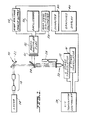
- a detection system 10 for use with an imaging screen 12, fabricated as will be described later herein.
- Screen 12 has been placed on an electrophoresis gel containing radioactively labelled, dye-tagged, or chemiluminescent labelled DNA, RNA or other protein fragments for exposure.
- the beta particles or visible light emitted by the labelled or tagged fragments impinge upon the surface of the imaging screen which is coated with an electron trapping material as described later.
- a laser 14 is utilized to scan the surface of the imaging screen by impinging a laser beam onto the electron trapping material in a row-by-row and column-by-column manner.
- the imaging screen in mounted on an x-y stepping stage 16 for that purpose.
- Laser 14 is preferably a 50 milliwatt Nd:Yag laser with an output having a wavelength centered about 1064 nm. Alternatively, a laser diode, with an output centered about 860 nm may be used in the present invention.
- laser 14 reads out the information stored in the electron trapping material. When it is desired to "erase” the impingement pattern stored in the electron trapping material, broad area infrared light produced by a filtered light source can be employed for the erasure.
- the output of laser 14 is controlled by a constant current power supply (not shown).
- the output from laser 14 is collimated by collimating optics 18 and then reflected by a IR mirror 22 through a cold mirror 24 and into a 20x microscope objective 20.
- a micrometer 26 is used to adjust the image of the laser beam down to less than a 20 micron spot on imaging screen 12.
- imaging screen 12 is mounted on ax-y stepping stage 16, such as that available from Aerotech, for serial scan-readout.
- An x-y translator controller 28 under command of a microcomputer 30, moves the x-y stepping stage 16 so that the trapped electron population is scanned by laser 14 in a pixel-by-pixel manner.
- the release of trapped electrons in the electron trapping material results in the emission of visible light, which travels back up through microscope objective 20 and is deflected by cold mirror 24 through a short pass filter 31 and into a visible light detector 32, preferably a photomultiplier tube such as Hamamatsu Model R268.
- visible light detector 32 can be a solid state image capture array, such as a CID or CCD, e.g., a Fairchild CID 2250 camera chip.
- CID or CCD e.g., a Fairchild CID 2250 camera chip.
- the entire surface of imaging screen 12 is illuminated with infrared light for read out; i.e. scanning is not necessary.
- infrared illumination is provided by an infrared flash 42.
- the infrared light passes through a cold mirror 44 and onto the imaging screen 12.
- Imaging screen 12 may be mounted in the film holder 46 of a camera back 48.
- the visible light emitted from the electron trapping material is reflected off cold mirror 44 and passes through an optical filter 50 and a lens 52 before entering a CID camera 54.
- Optical filter 50 is of the type that transmits visible light and blocks infrared light.
- Lens 52 is a 55mm f2.8 lens which focuses an image of imaging screen 12 onto CID camera 54.
- a light-tight enclosure 56 prevents external light from entering the optical portion of the system.
- the system of Fig. 2 is controlled by a microcomputer 56.
- microcomputer 56 controls CID camera 54 via a camera interface 58.
- Each frame of video information corresponding to the image received by CID camera 54 is collected by a frame grabber 60 (under control of microcomputer 56) and displayed on a gray scale video monitor 62.
- Frame grabber 60 also generates a signal for triggering infrared flash 42.
- Digital communication between microcomputer 56, camera interface 58 and frame grabber 62 occurs over a computer bus 64.
- a photomultiplier is used the visible light detector as shown in Fig. 1, it is powered by a high voltage power supply 34, and the output of the photomultiplier (an electrical signal proportional to the detected visible light input) is fed to an oscilloscope 36 (for visual display) and to a high speed digitizing voltmeter 38 (for A/D conversion). The digital output of digitizing voltmeter 38 is fed into microcomputer 30 for processing and conversion into an image which is displayed on graphics display
- the above-described system and its components are merely the preferred embodiment of the invention.
- many other types of infrared light sources, scanning systems and visible light detectors may be utilized to stimulate the charged electron trapping material in imaging screen 12 and to detect the visible light emitted therefrom.
- the preferred embodiment described above is capable of resolving a "pixel" size of 200 micrometers or smaller on the surface of imaging screen 12.
- the electron trapping material utilized in the present invention is a novel photoluminescent material which can be "charged” by the radiation or visible light to be measured; upon such energetic exposure, electrons in the material are raised to a higher energy state where they are “trapped” and stay indefinitely.
- low energy photons such as infrared
- the stored electrons are released from their traps, and, upon falling to a lower energy level, emit visible light which can be detected and measured.
- Fig. 3 shows the principles of operation of the electron trapping material used in the present invention.
- the basic crystalline photoluminescent material used has a valence band G full of electrons at a ground state.
- the material is subjected to radiation or visible light which functions to energize certain electrons in the valence band G.
- An electron shown on the left is originally in a valence band G and is subjected to charging radiation or visible light.
- the electron absorbs a beta particle or photon raising its energy level to a communication band E where communication takes place with other energized electrons resulting in transitions.
- the electron may drop back to a trapping level T or back to the valence band G depending upon the composition of the material and available trapping sites.
- the electron if in the trapping level T, will remain isolated from other electrons and trapped until sufficient additional energy is provided to the electron to raise its energy back up to the communication band E where it may interact with other electrons and undergo recombination causing it to move back to the valence band G and output a photon of visible light in the process.
- the number of trapping sites, the depth of the traps and the probability of transitions occuring in the communication band are all dependent upon the composition of the photoluminescent material used.
- the electron trapping material is formed of a strontium sulfide and/or calcium sulfide base combined with samarium metal or a samarium compound as a first dopant and either a europium compound or a cerium compound, or both, as a second dopant.
- Lithium fluoride is preferably added as a flux to provide fusibility, and barium sulfate can be used to improve the brightness of light output from the material.
- a cerium compound is used as a second dopant to provide an electron trapping material with improved sensitivity to beta particles.
- Examples of such electron trapping materials are disclosed in U.S. Patent No. 4,822,520, U.S. Patent No. 4,855,603, and U.S. Patent No. 4,812,660, the disclosures of which are herein incorporated by reference.
- the electron trapping materials of the first two patents emit blue-green light, while the material of the third patent emits a yellow-green light.
- a europium compound as the second dopant to provide an electron trapping material with a brighter output.
- Examples of europium doped electron trapping materials are disclosed in U.S. Patent No. 4,839,092, U.S. Patent No. 4,842,960 and U.S. Patent No. 4,879,186, the disclosures of which are herein incorporated by reference.
- the electron trapping materials of the first two patents emit orange light, while the material of the third patent emits a reddish-orange light.
- cerium and europium doped electron trapping materials described in the above-identified patents have electron traps on the order of approximately 1.0 eV.
- a thick or thin film of the electron trapping material may be applied to a substrate (e.g. vitreous quartz) to form the detector screen of the present invention.
- a substrate e.g. vitreous quartz
- the advantage of the thick film version (having a thickness on the order of hundreds of microns) is that all incoming flux, e.g. beta particles, is absorbed by the material and stored as energy in the form of trapped electrons.
- the advantage of the thin film version (having a thickness on the order of microns) is that very low energy beta particles such as from 3H can be detected with a higher signal to noise ratio.
- the electron trapping material is fused at a high temperature, ground, either attached or reheated at a lower temperature and then mixed with a binder and dispersed onto the substrate.
- the thin film version can be used where the flux emitted from the electrophoresis gel is of very low energy.
- the thin film version is prepared by physical vapor deposition of the fused material directly onto the substrate.
- Fig. 4 shows a cross-sectional view of an imaging screen 12 in which a film of electron trapping material 70 is disposed upon a substrate 72.
- a film of electron trapping material 70 is disposed upon a substrate 72.
- Any of a number of known materials having suitable properties may be used for the substrate 72.
- substrates that may be useful are: sapphire, alumina, other ceramics, quartz, fiber optic faceplates, other glasses, metals such as aluminum, various organic polymers, and polycarbonates.
- the material 70 establishes a planar surface 74 on substrate 72.
- An optional transparent coating 76 may encapsulate the material 70 and substrate 72.
Landscapes
- Chemical & Material Sciences (AREA)
- Life Sciences & Earth Sciences (AREA)
- Health & Medical Sciences (AREA)
- Engineering & Computer Science (AREA)
- Molecular Biology (AREA)
- Physics & Mathematics (AREA)
- Inorganic Chemistry (AREA)
- Materials Engineering (AREA)
- Organic Chemistry (AREA)
- Biochemistry (AREA)
- Electrochemistry (AREA)
- Analytical Chemistry (AREA)
- Chemical Kinetics & Catalysis (AREA)
- General Health & Medical Sciences (AREA)
- General Physics & Mathematics (AREA)
- Immunology (AREA)
- Pathology (AREA)
- Spectroscopy & Molecular Physics (AREA)
- Biophysics (AREA)
- Manufacturing & Machinery (AREA)
- Investigating, Analyzing Materials By Fluorescence Or Luminescence (AREA)
- Investigating Or Analysing Biological Materials (AREA)
- Luminescent Compositions (AREA)
- Measurement Of Radiation (AREA)
- Electroluminescent Light Sources (AREA)
- Optical Record Carriers And Manufacture Thereof (AREA)
Applications Claiming Priority (3)
| Application Number | Priority Date | Filing Date | Title |
|---|---|---|---|
| US07/184,263 US4915982A (en) | 1985-10-10 | 1988-04-21 | Method of making thin film photoluminescent articles |
| US07/383,534 US5028793A (en) | 1985-10-10 | 1989-07-24 | Imaging screen for electrophoresis applications |
| US383534 | 1989-07-24 |
Publications (2)
| Publication Number | Publication Date |
|---|---|
| EP0413962A1 true EP0413962A1 (de) | 1991-02-27 |
| EP0413962B1 EP0413962B1 (de) | 1996-12-27 |
Family
ID=36685797
Family Applications (2)
| Application Number | Title | Priority Date | Filing Date |
|---|---|---|---|
| EP89106286A Expired - Lifetime EP0338368B1 (de) | 1988-04-21 | 1989-04-10 | Photolumineszente Dünnschicht-Gegenstände und Methode zur Herstellung derselben |
| EP90113742A Expired - Lifetime EP0413962B1 (de) | 1988-04-21 | 1990-07-18 | Bilderzeugender Schirm für die Elektrophorese und Vorrichtung zur Bildwiedergabe |
Family Applications Before (1)
| Application Number | Title | Priority Date | Filing Date |
|---|---|---|---|
| EP89106286A Expired - Lifetime EP0338368B1 (de) | 1988-04-21 | 1989-04-10 | Photolumineszente Dünnschicht-Gegenstände und Methode zur Herstellung derselben |
Country Status (4)
| Country | Link |
|---|---|
| EP (2) | EP0338368B1 (de) |
| JP (2) | JPH0236296A (de) |
| AT (2) | ATE95549T1 (de) |
| DE (2) | DE68909658T2 (de) |
Cited By (1)
| Publication number | Priority date | Publication date | Assignee | Title |
|---|---|---|---|---|
| DE19509438A1 (de) * | 1994-03-18 | 1995-09-28 | Bio Rad Laboratories | Schutzüberzug für einen Leuchtstoff-Abbildungsschirm |
Families Citing this family (8)
| Publication number | Priority date | Publication date | Assignee | Title |
|---|---|---|---|---|
| JP2631759B2 (ja) * | 1990-06-04 | 1997-07-16 | 日本電信電話株式会社 | 赤外可視変換蛍光体 |
| US5532199A (en) * | 1992-06-19 | 1996-07-02 | Mitsubishi Rayon Co., Ltd. | Carrier-supported catalyst for the synthesis of unsaturated aldehydes and unsaturated carboxylic acids and process for preparing the same |
| HK1040413A1 (en) * | 1998-11-27 | 2002-06-07 | Nittetsu Mining Co., Ltd. | Fluorescent or phosphorescent composition |
| US6572095B1 (en) | 1999-09-03 | 2003-06-03 | Fuji Photo Film Co., Ltd. | Method of and system for conveying sheet to be scanned |
| US6162490A (en) * | 1999-09-07 | 2000-12-19 | Iomega Corporation | Method for applying an emissive material to a substrate |
| GB0208481D0 (en) * | 2002-04-12 | 2002-05-22 | Btg Int Ltd | Photonic phosphors and devices |
| JP2006314923A (ja) | 2005-05-12 | 2006-11-24 | Nippon Kayaku Co Ltd | メタクリル酸製造用触媒の製造方法 |
| JP5570142B2 (ja) | 2009-05-26 | 2014-08-13 | 日本化薬株式会社 | メタクリル酸製造触媒の製造方法およびメタクリル酸の製造方法 |
Citations (3)
| Publication number | Priority date | Publication date | Assignee | Title |
|---|---|---|---|---|
| EP0126218A2 (de) * | 1983-02-24 | 1984-11-28 | Fuji Photo Film Co., Ltd. | Anregbare Phosphorschicht mit einer hydrophilen Schutzschicht |
| EP0159523A1 (de) * | 1984-03-15 | 1985-10-30 | Fuji Photo Film Co., Ltd. | Verfahren zur Autoradiographie |
| US4839092A (en) * | 1985-10-10 | 1989-06-13 | Quantex Corporation | Photoluminescent materials for outputting orange light |
Family Cites Families (6)
| Publication number | Priority date | Publication date | Assignee | Title |
|---|---|---|---|---|
| US2521124A (en) * | 1946-08-09 | 1950-09-05 | Neville F Miller | Infrared strontium sulfide phosphors |
| JPS4948835A (de) * | 1972-09-14 | 1974-05-11 | ||
| EP0180602B1 (de) * | 1984-04-24 | 1989-03-01 | Alternative Energy Research Centre, Inc. | Infrarotempfindliches phosphor und dessen herstellung |
| JPH06100679B2 (ja) * | 1985-08-26 | 1994-12-12 | コニカ株式会社 | 放射線画像変換パネルの製造方法 |
| US4755324A (en) * | 1985-11-15 | 1988-07-05 | Quantex Corporation | Thermoluminescent material |
| JPH0654360B2 (ja) * | 1987-07-13 | 1994-07-20 | コニカ株式会社 | 放射線画像変換パネルの製造方法 |
-
1989
- 1989-04-10 AT AT89106286T patent/ATE95549T1/de not_active IP Right Cessation
- 1989-04-10 EP EP89106286A patent/EP0338368B1/de not_active Expired - Lifetime
- 1989-04-10 DE DE89106286T patent/DE68909658T2/de not_active Expired - Fee Related
- 1989-04-21 JP JP1103289A patent/JPH0236296A/ja active Pending
-
1990
- 1990-07-18 AT AT90113742T patent/ATE146894T1/de active
- 1990-07-18 DE DE69029492T patent/DE69029492T2/de not_active Expired - Fee Related
- 1990-07-18 EP EP90113742A patent/EP0413962B1/de not_active Expired - Lifetime
- 1990-07-19 JP JP19185390A patent/JP3297874B2/ja not_active Expired - Fee Related
Patent Citations (3)
| Publication number | Priority date | Publication date | Assignee | Title |
|---|---|---|---|---|
| EP0126218A2 (de) * | 1983-02-24 | 1984-11-28 | Fuji Photo Film Co., Ltd. | Anregbare Phosphorschicht mit einer hydrophilen Schutzschicht |
| EP0159523A1 (de) * | 1984-03-15 | 1985-10-30 | Fuji Photo Film Co., Ltd. | Verfahren zur Autoradiographie |
| US4839092A (en) * | 1985-10-10 | 1989-06-13 | Quantex Corporation | Photoluminescent materials for outputting orange light |
Cited By (1)
| Publication number | Priority date | Publication date | Assignee | Title |
|---|---|---|---|---|
| DE19509438A1 (de) * | 1994-03-18 | 1995-09-28 | Bio Rad Laboratories | Schutzüberzug für einen Leuchtstoff-Abbildungsschirm |
Also Published As
| Publication number | Publication date |
|---|---|
| JPH03205550A (ja) | 1991-09-09 |
| DE69029492T2 (de) | 1997-04-10 |
| EP0338368A1 (de) | 1989-10-25 |
| ATE95549T1 (de) | 1993-10-15 |
| JPH0236296A (ja) | 1990-02-06 |
| EP0413962B1 (de) | 1996-12-27 |
| DE68909658D1 (de) | 1993-11-11 |
| EP0338368B1 (de) | 1993-10-06 |
| DE68909658T2 (de) | 1994-02-10 |
| JP3297874B2 (ja) | 2002-07-02 |
| ATE146894T1 (de) | 1997-01-15 |
| DE69029492D1 (de) | 1997-02-06 |
Similar Documents
| Publication | Publication Date | Title |
|---|---|---|
| US5028793A (en) | Imaging screen for electrophoresis applications | |
| US4889990A (en) | Method and apparatus for recording and reproducing electron microscope image | |
| DE69724523T2 (de) | Bildlesegerät | |
| US4665312A (en) | Signal detecting method in autoradiography | |
| US4651220A (en) | Method of recording and reproducing images produced by an electron microscope | |
| JPH09504107A (ja) | 改良された結像方法および装置 | |
| JPH1021373A (ja) | 画像解析装置 | |
| US5030834A (en) | Fiber optic dosimeter system using electron trapping materials | |
| EP0413962B1 (de) | Bilderzeugender Schirm für die Elektrophorese und Vorrichtung zur Bildwiedergabe | |
| US4933558A (en) | X-ray sensitive area detection device | |
| KR100721754B1 (ko) | 광학적으로 투명한 형광체를 사용한 고 해상도 이미징시스템 및 그 방법 | |
| US5124558A (en) | Imaging system for mamography employing electron trapping materials | |
| GB2246197A (en) | Detection and imaging in biochemical assays using phosphorescent screens | |
| US5796113A (en) | Methods and apparatus for recording and reading-out an ionization radiation image | |
| US5672514A (en) | Chemiluminescent detecting method and apparatus | |
| US6507426B2 (en) | Scanner apparatus | |
| US4694171A (en) | Electron microscope image focusing using instantaneous emission of stimulable phosphor sheet | |
| JP3474765B2 (ja) | 画像記録・読み取りシステム | |
| EP0181507B1 (de) | Vorrichtung zur Aufzeichnung eines Bildes mittels eines Elektronenmikroskops | |
| US6343142B1 (en) | Image analyzing apparatus | |
| EP0178672B1 (de) | Elektronenmikroskop | |
| WO2000010033A1 (en) | Methods and apparatus for recording and reading-out an image formed by ionizing radiation | |
| US4801801A (en) | Transmission-type electron microscope | |
| Sutherland | Electronic imaging systems for quantitative electrophoresis of DNA | |
| EP0677823A1 (de) | Vorrichtung zur Bildanalyse |
Legal Events
| Date | Code | Title | Description |
|---|---|---|---|
| PUAI | Public reference made under article 153(3) epc to a published international application that has entered the european phase |
Free format text: ORIGINAL CODE: 0009012 |
|
| AK | Designated contracting states |
Kind code of ref document: A1 Designated state(s): AT BE CH DE DK ES FR GB GR IT LI LU NL SE |
|
| 17P | Request for examination filed |
Effective date: 19910613 |
|
| 17Q | First examination report despatched |
Effective date: 19931108 |
|
| GRAG | Despatch of communication of intention to grant |
Free format text: ORIGINAL CODE: EPIDOS AGRA |
|
| GRAH | Despatch of communication of intention to grant a patent |
Free format text: ORIGINAL CODE: EPIDOS IGRA |
|
| GRAH | Despatch of communication of intention to grant a patent |
Free format text: ORIGINAL CODE: EPIDOS IGRA |
|
| GRAA | (expected) grant |
Free format text: ORIGINAL CODE: 0009210 |
|
| AK | Designated contracting states |
Kind code of ref document: B1 Designated state(s): AT BE CH DE DK ES FR GB GR IT LI LU NL SE |
|
| PG25 | Lapsed in a contracting state [announced via postgrant information from national office to epo] |
Ref country code: GR Free format text: LAPSE BECAUSE OF FAILURE TO SUBMIT A TRANSLATION OF THE DESCRIPTION OR TO PAY THE FEE WITHIN THE PRESCRIBED TIME-LIMIT Effective date: 19961227 Ref country code: ES Free format text: THE PATENT HAS BEEN ANNULLED BY A DECISION OF A NATIONAL AUTHORITY Effective date: 19961227 Ref country code: DK Effective date: 19961227 Ref country code: NL Free format text: LAPSE BECAUSE OF FAILURE TO SUBMIT A TRANSLATION OF THE DESCRIPTION OR TO PAY THE FEE WITHIN THE PRESCRIBED TIME-LIMIT Effective date: 19961227 Ref country code: BE Effective date: 19961227 Ref country code: AT Effective date: 19961227 |
|
| REF | Corresponds to: |
Ref document number: 146894 Country of ref document: AT Date of ref document: 19970115 Kind code of ref document: T |
|
| REG | Reference to a national code |
Ref country code: CH Ref legal event code: NV Representative=s name: DIETLIN & CIE S.A. |
|
| REF | Corresponds to: |
Ref document number: 69029492 Country of ref document: DE Date of ref document: 19970206 |
|
| ITF | It: translation for a ep patent filed | ||
| PG25 | Lapsed in a contracting state [announced via postgrant information from national office to epo] |
Ref country code: SE Effective date: 19970327 |
|
| ET | Fr: translation filed | ||
| NLV1 | Nl: lapsed or annulled due to failure to fulfill the requirements of art. 29p and 29m of the patents act | ||
| PG25 | Lapsed in a contracting state [announced via postgrant information from national office to epo] |
Ref country code: LU Free format text: LAPSE BECAUSE OF NON-PAYMENT OF DUE FEES Effective date: 19970731 |
|
| PLBE | No opposition filed within time limit |
Free format text: ORIGINAL CODE: 0009261 |
|
| STAA | Information on the status of an ep patent application or granted ep patent |
Free format text: STATUS: NO OPPOSITION FILED WITHIN TIME LIMIT |
|
| 26N | No opposition filed | ||
| REG | Reference to a national code |
Ref country code: CH Ref legal event code: PUE Owner name: QUANTEX CORPORATION TRANSFER- INSTITUTE FOR RADIOL |
|
| REG | Reference to a national code |
Ref country code: GB Ref legal event code: 732E |
|
| REG | Reference to a national code |
Ref country code: GB Ref legal event code: IF02 |
|
| PGFP | Annual fee paid to national office [announced via postgrant information from national office to epo] |
Ref country code: GB Payment date: 20050713 Year of fee payment: 16 |
|
| PGFP | Annual fee paid to national office [announced via postgrant information from national office to epo] |
Ref country code: FR Payment date: 20050718 Year of fee payment: 16 |
|
| PGFP | Annual fee paid to national office [announced via postgrant information from national office to epo] |
Ref country code: CH Payment date: 20050721 Year of fee payment: 16 |
|
| PGFP | Annual fee paid to national office [announced via postgrant information from national office to epo] |
Ref country code: DE Payment date: 20050831 Year of fee payment: 16 |
|
| PG25 | Lapsed in a contracting state [announced via postgrant information from national office to epo] |
Ref country code: GB Free format text: LAPSE BECAUSE OF NON-PAYMENT OF DUE FEES Effective date: 20060718 |
|
| PG25 | Lapsed in a contracting state [announced via postgrant information from national office to epo] |
Ref country code: CH Free format text: LAPSE BECAUSE OF NON-PAYMENT OF DUE FEES Effective date: 20060731 Ref country code: LI Free format text: LAPSE BECAUSE OF NON-PAYMENT OF DUE FEES Effective date: 20060731 |
|
| PGFP | Annual fee paid to national office [announced via postgrant information from national office to epo] |
Ref country code: IT Payment date: 20060731 Year of fee payment: 17 |
|
| PG25 | Lapsed in a contracting state [announced via postgrant information from national office to epo] |
Ref country code: DE Free format text: LAPSE BECAUSE OF NON-PAYMENT OF DUE FEES Effective date: 20070201 |
|
| REG | Reference to a national code |
Ref country code: CH Ref legal event code: PL |
|
| GBPC | Gb: european patent ceased through non-payment of renewal fee |
Effective date: 20060718 |
|
| REG | Reference to a national code |
Ref country code: FR Ref legal event code: ST Effective date: 20070330 |
|
| PG25 | Lapsed in a contracting state [announced via postgrant information from national office to epo] |
Ref country code: FR Free format text: LAPSE BECAUSE OF NON-PAYMENT OF DUE FEES Effective date: 20060731 |
|
| PG25 | Lapsed in a contracting state [announced via postgrant information from national office to epo] |
Ref country code: IT Free format text: LAPSE BECAUSE OF NON-PAYMENT OF DUE FEES Effective date: 20070718 |