EP0414317A2 - Dispositif d'onduleur - Google Patents
Dispositif d'onduleur Download PDFInfo
- Publication number
- EP0414317A2 EP0414317A2 EP90202233A EP90202233A EP0414317A2 EP 0414317 A2 EP0414317 A2 EP 0414317A2 EP 90202233 A EP90202233 A EP 90202233A EP 90202233 A EP90202233 A EP 90202233A EP 0414317 A2 EP0414317 A2 EP 0414317A2
- Authority
- EP
- European Patent Office
- Prior art keywords
- pulse
- resonant circuit
- current
- circuit current
- blocking
- Prior art date
- Legal status (The legal status is an assumption and is not a legal conclusion. Google has not performed a legal analysis and makes no representation as to the accuracy of the status listed.)
- Withdrawn
Links
Images
Classifications
-
- H—ELECTRICITY
- H02—GENERATION; CONVERSION OR DISTRIBUTION OF ELECTRIC POWER
- H02M—APPARATUS FOR CONVERSION BETWEEN AC AND AC, BETWEEN AC AND DC, OR BETWEEN DC AND DC, AND FOR USE WITH MAINS OR SIMILAR POWER SUPPLY SYSTEMS; CONVERSION OF DC OR AC INPUT POWER INTO SURGE OUTPUT POWER; CONTROL OR REGULATION THEREOF
- H02M7/00—Conversion of AC power input into DC power output; Conversion of DC power input into AC power output
- H02M7/42—Conversion of DC power input into AC power output without possibility of reversal
- H02M7/44—Conversion of DC power input into AC power output without possibility of reversal by static converters
- H02M7/48—Conversion of DC power input into AC power output without possibility of reversal by static converters using discharge tubes with control electrode or semiconductor devices with control electrode
- H02M7/505—Conversion of DC power input into AC power output without possibility of reversal by static converters using discharge tubes with control electrode or semiconductor devices with control electrode using devices of a thyratron or thyristor type requiring extinguishing means
- H02M7/515—Conversion of DC power input into AC power output without possibility of reversal by static converters using discharge tubes with control electrode or semiconductor devices with control electrode using devices of a thyratron or thyristor type requiring extinguishing means using semiconductor devices only
- H02M7/523—Conversion of DC power input into AC power output without possibility of reversal by static converters using discharge tubes with control electrode or semiconductor devices with control electrode using devices of a thyratron or thyristor type requiring extinguishing means using semiconductor devices only with LC-resonance circuit in the main circuit
- H02M7/5233—Conversion of DC power input into AC power output without possibility of reversal by static converters using discharge tubes with control electrode or semiconductor devices with control electrode using devices of a thyratron or thyristor type requiring extinguishing means using semiconductor devices only with LC-resonance circuit in the main circuit the commutation elements being in a push-pull arrangement
- H02M7/5236—Conversion of DC power input into AC power output without possibility of reversal by static converters using discharge tubes with control electrode or semiconductor devices with control electrode using devices of a thyratron or thyristor type requiring extinguishing means using semiconductor devices only with LC-resonance circuit in the main circuit the commutation elements being in a push-pull arrangement in a series push-pull arrangement
-
- H—ELECTRICITY
- H05—ELECTRIC TECHNIQUES NOT OTHERWISE PROVIDED FOR
- H05G—X-RAY TECHNIQUE
- H05G1/00—X-ray apparatus involving X-ray tubes; Circuits therefor
- H05G1/08—Electrical details
- H05G1/10—Power supply arrangements for feeding the X-ray tube
- H05G1/20—Power supply arrangements for feeding the X-ray tube with high-frequency AC; with pulse trains
Definitions
- the invention relates to an inverter arrangement, in particular for an X-ray generator, with a series oscillating circuit and at least two electronic switches through which a half oscillation of the oscillating circuit current flows and which are switched in push-pull manner and via which the series oscillating circuit can be coupled to a DC voltage source.
- Such inverters are known (DE-OS 3046 413; DE-OS 30 46 767 and DE-OS 32 18 535).
- the electronic switches are each conductive during one half-oscillation, and the electrical power that can be generated by such an inverter is greater the closer the half-oscillations follow one another, which flow through the electronic switches in push-pull.
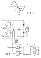
- the electronic switches are formed by thyristors, which are connected in the forward direction to the DC voltage source and each of which has a diode connected in anti-parallel. With such electronic switches, it is not possible to let the semi-oscillations flow one after the other through the push-pull switches, as can be seen in FIG. 1, which shows the time course of the resonant circuit current in the known inverter arrangement. It is assumed that a thyristor is conductive during the one positive half-oscillation. After the current has passed through zero, the diode connected in parallel with the thyristor initially takes over the ring-back current and the ignited thyristor loses its current Conductivity. As a result of the active power delivered to the consumer, the negative half-oscillation of the return oscillation current (indicated partly by dashed lines in FIG. 1) has a smaller amplitude than the positive half-oscillation.
- the push-pull controlled thyristor may only be fired if the so-called free time (tq), which is required for the removal of the charge carriers, has elapsed after the zero current has passed through the previously conductive thyristor.
- tq free time
- the ignition pulse can be generated with the aid of a delay circuit which is started by the current zero crossing.
- a comparator circuit is generally provided, the input of which is supplied with a value proportional to the instantaneous resonant circuit current and which responds as soon as the resonant circuit current has dropped below a value i s .
- This value i s must be large enough to prevent interference signals superimposed on the measurement signal from starting the delay circuit and thus possibly triggering the premature generation of the ignition pulses. Between the extinction of the one thyristor, at least a period of time must elapse that corresponds to the sum of the release time and the time within which the ringing current reaches the value i s after the current zero crossing. In the case of a particularly large load or a particularly large output of active power, it may even happen that the oscillation current does not reach the value i s , so that the ignition pulse starting the next half oscillation cannot be generated. This results in voltage or current drops in the load.
- the object of the present invention is to design an inverter of the type mentioned at the outset in such a way that the period within which the resonant circuit current passes from one electronic switch to the other can be shortened, so that the power which can be output is increased.
- GTO thyristors serve as electronic switches, which are connected by a pulse generator arrangement which generates a blocking pulse in the region of the zero crossing of the resonant circuit current and by means of which an ignition pulse for the subsequently conducting GTO thyristor after a defined delay time can be generated after the blocking pulse takes effect.
- GTO Gate Turn Off
- the invention takes advantage of the fact that in an inverter of the type mentioned at the outset, the current flowing through the electronic switching elements tends towards a zero crossing in a sinusoidal manner. In the area of the zero crossing of the resonant circuit current, however, the current-carrying GTO thyristor can operate with a relatively low-power lock impulses are blocked. A weak pulse generator is sufficient for this. As such, a GTO thyristor no longer conducts after the current through it has passed zero. However, the blocking pulse accelerates the charge carrier breakdown in the GTO thyristor and thus considerably shortens the release time. The ignition pulse for the next GTO thyristor can then follow the blocking pulse at the shortest possible time interval, so that there is hardly any gap between the two half-oscillations.
- the blocking pulse does not have to start exactly at the zero crossing of the resonant circuit current; it can also be a little earlier (up to 2% of the period), i.e. in the area of the zero crossing.
- the blocking pulses are delivered even further before the zero crossing by a relatively high-resistance pulse generator, they are practically short-circuited by the then very low-resistance gate-cathode path of the GTO thyristor. This only changes when the mentioned route becomes high-resistance. Although the blocking pulse starts relatively early in this case, it only becomes effective in the area of the zero crossing.
- a simpler embodiment of the invention provides that a measuring device for the resonant circuit current is provided, which is coupled to a comparator circuit which responds when the resonant circuit current falls below a reference value, and that the pulse generator arrangement is controlled by the comparator circuit in such a way that the blocking pulse is generated with a defined delay after falling below the reference value. It is therefore not necessary to measure the conductivity of the gate-cathode path of the GTO thyristors, but only the resonant circuit current, which must be measured anyway for control purposes.
- the time course of the active oscillation current half-wave - unlike the course of the return oscillation current - is largely independent of the load on the inverter.
- the timing of the blocking pulse and, subsequently, the timing of the ignition pulse for the other GTO thyristor - in each case based on the zero crossing of the resonant circuit current - do not depend on the load.
- a DC voltage is supplied to the inverter shown in FIG. 2, which can be generated from an AC voltage, for example by rectification (not shown in more detail).
- the series connection of two capacitors 1 and 2 of the same size is connected to the DC voltage, and the series connection of two electronic switches is connected in parallel.
- Each switch consists of a GTO thyristor 3 or 4 and a diode 5 or 6 connected antiparallel to it.
- connection points of the switches 3, 5 and 4,6 on the one hand and the capacitors 1,2 on the other hand are connected to one another via a bridge arm which comprises the series connection of the primary windings of a current transformer 7 for measuring the actual value of the resonant circuit current and a heating transformer 8, to the secondary winding of which the filament of an X-ray tube 9 is connected.
- the heating transformer is designed for the separation of the potentials on its primary side (almost earth potential) and its secondary side (negative high-voltage potential) and therefore has a relatively large leakage inductance, which together with the capacitors 1 and 2 has a series resonance circuit with a series resonance frequency of e.g. 15 kHz forms.
- a series resonance frequency e.g. 15 kHz forms.
- an oscillating circuit current flows through the capacitors 1 and 2, the primary winding 8 and the GTO thyristor 4, and in the other half oscillation a current flows through the GTO thyristor 3, the primary winding 8 and the capacitors 1 and 2.
- a resistor 10 is connected to the secondary winding of the current transformer 7.
- the voltage across this resistor is proportional to the instantaneous value of the current through the primary winding 8.
- the controller 11 compares the setpoint I o of the heating current with the effective value of the measured current (to generate this effective value from the instantaneous value at the resistor 10, an RMS module (not shown in more detail) must be available to generate the effective value be) and provides an output signal that depends on the difference between these values.
- the window comparator 12 responds as soon as the instantaneous value of the current has dropped below a value i s .
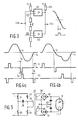
- the structure of this window comparator is shown in Fig. 3.
- the comparator comprises two amplifiers 121 and 122 with a high-resistance output, to which the voltage across the resistor 10 is supplied.
- the non-inverting inputs of the amplifiers 121 and 122 are connected to the tap of a voltage divider 123 connected between ground and the positive supply voltage V + or to the signal input of the comparator.
- the inverting inputs of the amplifiers 121 and 122 are connected to the signal input and the tap of a further voltage divider 124 connected between ground and the negative supply voltage V.
- the outputs of the two amplifiers 121, 122 are connected to one another and to the positive supply voltage V + via a resistor 125. These outputs also form the output of the window comparator.
- amplifier 121 receives a current (amplifier 122 is blocked) so that the common output has a low potential. If the voltage at the common input falls below the voltage at the tap of the potentiometer 123 (in this case the resonant circuit current has dropped below the value i s ), then the amplifier 121 also no longer delivers current. Only after the common input voltage has fallen below a negative value that corresponds to the voltage at the tap of the potentiometer 124, the amplifier 122 supplies a current. The window comparator thus delivers a positive pulse at each zero crossing of the resonant circuit current (in both directions), the leading edge of which is used to generate a blocking pulse.
- the controller 11 and the window comparator 12 control a trigger circuit 13 which, similar to the trigger circuits for thyristors and others.
- the blocking pulses begin after a defined delay time after the leading edge of the pulses supplied by the window comparator 12.
- the trigger circuit has two outputs, which are coupled via pulse transmitters 14 and 15 to the gate-cathode sections of the GTO thyristors 3 and 4, respectively.
- the first (positive) half oscillation of the resonant circuit current Mes is initiated by an ignition pulse for the associated GTO thyristor (eg 3) (voltage u 1) after the other GTO thyristor (4) has been blocked.
- the firing pulse must last at least as long that the resonant circuit current has exceeded the value of the latching current before the firing pulse ends. After the half oscillation has passed its maximum (e.g.
- the window comparator delivers a positive pulse, which within the trigger circuit causes a blocking pulse to be generated which has the opposite polarity to the previous ignition pulse , and whose leading edge is offset from the leading edge of the pulse supplied by the window comparator 12 by a defined delay time t d .
- t d 0.6 microseconds at the specified value i s is a favorable value which results from the delay times of the trigger circuit 13 and the pulse transmitter 14, 15 - that is to say without an additional delay element.
- the blocking pulse is timed so that it does not terminate the half-oscillation prematurely, but on the other hand the charge carriers are removed from the blocked GTO thyristor as soon as possible after the zero crossing of the resonant circuit current.
- the GTO thyristor 4 After blocking the thyristor 3, the GTO thyristor 4 is ignited (with u2). A period must elapse between the leading edges of the blocking pulse for the GTO thyristor 3 and the ignition pulse for the GTO thyristor 4, which corresponds at least to the greatest possible release time t q . With a suitable adaptation between the threshold values i s , t d and t q it can be achieved that the subsequent negative half-oscillation together with the previous positive half-oscillation results in an almost sinusoidal current curve.
- a blocking pulse for the GTO thyristor 4 follows, followed by an ignition pulse for the GTO thyristor 3 again with the delay time mentioned.
- the blocking pulses can be made so wide that they overlap with the ignition pulses, as long as it is ensured that the required delay (t q ) exists between the blocking pulse for one GTO thyristor and the ignition pulse for the other GTO thyristor.
- FIGS. 4a and 4b show that the blocking pulses are always generated - with a delay - regardless of the output power, when the amount of the current drops below the value i s .
- an ignition pulse can be generated for the other GTO thyristor (as in FIG. 4a), but this pulse can also be generated later, as in FIG. 4b.
- the inverter comprises two switching branches connected in parallel to the supply voltage terminals + and -, each of which consists of the series connection of two electronic switching elements 21 and 22 or 23 and 24.
- Each of these electronic switching elements consists of a GTO thyristor and an anti-parallel diode.
- the series connection of a capacitor 25 and the primary winding 26 of a high-voltage transformer 27 is connected between the connection points of the switching elements 21 and 22 on the one hand and the switching elements 23 and 24 on the other hand. This has a relatively large leakage inductance which, together with the capacitor 25, forms a series resonance circuit.
- the high-voltage transformer 27 has two secondary windings 28 and 29, respectively, which feed a rectifier 30 and 31, respectively, for generating a positive or negative high voltage, which is smoothed by capacitors 32 and 33 and which is supplied to the anode or the cathode of the X-ray tube 9.
- the switching elements 21 and 24 located in the bridge diagonal are each supplied with the same pulse voltage, if one disregards the required potential offset.
- the resonant circuit current flows through elements 25, 26, i.e. via switches 21 and 24, and in the other half oscillation, via switches 22 and 23.
- the series resonant inverter delivers its maximum power when the GTO thyristors in the electronic Switches are blocked shortly before reaching zero crossing and after the shortened release time the GTO thyristors located in the respective other current path are ignited.
Landscapes
- Engineering & Computer Science (AREA)
- Power Engineering (AREA)
- X-Ray Techniques (AREA)
- Inverter Devices (AREA)
Applications Claiming Priority (2)
| Application Number | Priority Date | Filing Date | Title |
|---|---|---|---|
| DE3927888A DE3927888A1 (de) | 1989-08-24 | 1989-08-24 | Wechselrichteranordnung |
| DE3927888 | 1989-08-24 |
Publications (2)
| Publication Number | Publication Date |
|---|---|
| EP0414317A2 true EP0414317A2 (fr) | 1991-02-27 |
| EP0414317A3 EP0414317A3 (en) | 1991-05-22 |
Family
ID=6387727
Family Applications (1)
| Application Number | Title | Priority Date | Filing Date |
|---|---|---|---|
| EP19900202233 Withdrawn EP0414317A3 (en) | 1989-08-24 | 1990-08-20 | Inverter device |
Country Status (4)
| Country | Link |
|---|---|
| US (1) | US5121317A (fr) |
| EP (1) | EP0414317A3 (fr) |
| JP (1) | JPH03110797A (fr) |
| DE (1) | DE3927888A1 (fr) |
Cited By (2)
| Publication number | Priority date | Publication date | Assignee | Title |
|---|---|---|---|---|
| EP0448165A3 (en) * | 1990-03-21 | 1992-01-22 | Philips Patentverwaltung Gmbh | Series resonant inverter, especially for an x-ray generator |
| WO2006092411A1 (fr) * | 2005-03-01 | 2006-09-08 | Basf Aktiengesellschaft | 5,6-dialkyl-7-amino-azolopyrimidines, leurs procedes de production, leur utilisation pour lutter contre des champignons nuisibles, et agents les contenant |
Families Citing this family (22)
| Publication number | Priority date | Publication date | Assignee | Title |
|---|---|---|---|---|
| SE500507C2 (sv) * | 1991-10-03 | 1994-07-04 | Alfa Laval Agri Int | Sätt att mäta utspänningen på ett elstängsel och elsträngselapparat för genomförande av sättet |
| DE69413856T2 (de) * | 1993-01-20 | 1999-05-12 | Koninklijke Philips Electronics N.V., Eindhoven | Röntgeneinrichtung |
| DE4334592C1 (de) * | 1993-10-11 | 1994-07-21 | Siemens Ag | Hochfrequenz-Generator |
| FR2758019B1 (fr) * | 1996-12-30 | 1999-01-22 | Alsthom Cge Alcatel | Convertisseur de puissance a commande amelioree des commutateurs principaux |
| DE19961541A1 (de) * | 1999-12-20 | 2001-07-19 | Magnet Motor Gmbh | Hochspannungswandler |
| US7295232B2 (en) | 2003-01-15 | 2007-11-13 | Canon Kabushiki Kaisha | Camera and program |
| JP4181923B2 (ja) | 2003-05-29 | 2008-11-19 | キヤノン株式会社 | 撮像装置および撮像装置の制御方法 |
| JP4136793B2 (ja) | 2003-05-29 | 2008-08-20 | キヤノン株式会社 | 撮像装置および撮像装置の制御方法 |
| JP4164424B2 (ja) * | 2003-08-29 | 2008-10-15 | キヤノン株式会社 | 撮像装置及び方法 |
| JP2006050457A (ja) | 2004-08-06 | 2006-02-16 | Canon Inc | 撮像装置 |
| EP1856122A2 (fr) * | 2005-03-02 | 2007-11-21 | Basf Aktiengesellschaft | 7-amino-azolopyrimidine 2-substituee, son procede de fabrication et son utilisation pour lutter contre les champignons nuisibles, et agents renfermant ce compose |
| BRPI0608712A2 (pt) * | 2005-03-18 | 2010-12-07 | Basf Ag | processo para a preparação de composto, e, uso do composto |
| EP2013963B1 (fr) * | 2006-04-25 | 2012-08-01 | Philips Intellectual Property & Standards GmbH | Dispositif de commande d'un convertisseur de puissance pour la détermination du point de commutation |
| CN101583613A (zh) * | 2007-01-11 | 2009-11-18 | 巴斯夫欧洲公司 | 生产芳基取代的稠合嘧啶的方法 |
| JP2009017078A (ja) * | 2007-07-03 | 2009-01-22 | Fujifilm Corp | ディジタル・スチル・カメラおよびその動作制御方法 |
| IT1393717B1 (it) * | 2009-03-31 | 2012-05-08 | Meta System Spa | Dispositivo e metodo per la conversione di corrente continua in corrente alternata |
| US9129414B2 (en) | 2011-10-14 | 2015-09-08 | Morpho, Inc. | Image compositing apparatus, image compositing method, image compositing program, and recording medium |
| JP6372182B2 (ja) * | 2014-06-17 | 2018-08-15 | 富士通株式会社 | 信号変換回路および電源装置 |
| CN110178445B (zh) | 2017-01-23 | 2022-10-21 | 昕诺飞控股有限公司 | 用于确定可调光脉冲led灯串的健康状态的系统和方法 |
| US11103207B1 (en) * | 2017-12-28 | 2021-08-31 | Radiation Monitorng Devices, Inc. | Double-pulsed X-ray source and applications |
| US11751316B2 (en) * | 2019-11-05 | 2023-09-05 | Gulmay Limited | Power transfer and monitoring devices for X-ray tubes |
| JP7577572B2 (ja) * | 2021-03-03 | 2024-11-05 | 富士フイルム株式会社 | 放射線管及び放射線源 |
Family Cites Families (14)
| Publication number | Priority date | Publication date | Assignee | Title |
|---|---|---|---|---|
| DE3046413A1 (de) * | 1980-12-10 | 1982-07-29 | Philips Patentverwaltung Gmbh, 2000 Hamburg | "roentgendiagnostikgenerator" |
| DE3046767A1 (de) * | 1980-12-12 | 1982-07-15 | Philips Patentverwaltung Gmbh, 2000 Hamburg | Roentgengenerator mit zwei wechselrichtern zur speisung der beiden statorwicklungen eines drehanoden-antriebsmotors |
| DE3218535A1 (de) * | 1982-05-17 | 1983-11-17 | Philips Patentverwaltung | Hochspannungserzeuger, insbesondere zur speisung einer roentgenroehre |
| US4460949A (en) * | 1982-09-30 | 1984-07-17 | General Electric Company | High frequency parallel resonant dc-dc converter |
| JPS6070698A (ja) * | 1983-09-27 | 1985-04-22 | Toshiba Corp | X線管フイラメント加熱装置 |
| US4653082A (en) * | 1984-01-18 | 1987-03-24 | Kabushiki Kaisha Toshiba | High voltage generating device for X-ray apparatus |
| JPS6116498A (ja) * | 1984-07-03 | 1986-01-24 | Toshiba Corp | X線高電圧発生装置 |
| DE3579556D1 (de) * | 1984-11-09 | 1990-10-11 | Leybold Ag | Wechselrichter mit einer last, die eine wechselrichter-ausgangsspannung bestimmter kurvenform und frequenz erzwingt. |
| JPS61161698A (ja) * | 1985-01-09 | 1986-07-22 | Hitachi Medical Corp | インバ−タ式x線装置 |
| US4587604A (en) * | 1985-02-06 | 1986-05-06 | Reliance Electric Company | Power supply employing low power and high power series resonant converters |
| DE3612524A1 (de) * | 1985-04-15 | 1986-10-23 | Hitachi Medical Corp., Tokio/Tokyo | Energieversorgungsvorrichtung mit wechselrichterstufe |
| FR2597285B1 (fr) * | 1986-04-11 | 1988-06-17 | Thomson Cgr | Dispositif d'alimentation en courant d'un filament de tube radiogene |
| JPH01144361A (ja) * | 1987-11-30 | 1989-06-06 | Toshiba Corp | 電力供給装置 |
| US4959558A (en) * | 1988-03-31 | 1990-09-25 | U.S. Philips Corporation | Circuit arrangement for detecting cross-over by an alternating voltage of a fixed reference voltage level |
-
1989
- 1989-08-24 DE DE3927888A patent/DE3927888A1/de not_active Withdrawn
-
1990
- 1990-08-13 US US07/566,738 patent/US5121317A/en not_active Expired - Fee Related
- 1990-08-20 EP EP19900202233 patent/EP0414317A3/de not_active Withdrawn
- 1990-08-21 JP JP2219902A patent/JPH03110797A/ja active Pending
Cited By (2)
| Publication number | Priority date | Publication date | Assignee | Title |
|---|---|---|---|---|
| EP0448165A3 (en) * | 1990-03-21 | 1992-01-22 | Philips Patentverwaltung Gmbh | Series resonant inverter, especially for an x-ray generator |
| WO2006092411A1 (fr) * | 2005-03-01 | 2006-09-08 | Basf Aktiengesellschaft | 5,6-dialkyl-7-amino-azolopyrimidines, leurs procedes de production, leur utilisation pour lutter contre des champignons nuisibles, et agents les contenant |
Also Published As
| Publication number | Publication date |
|---|---|
| US5121317A (en) | 1992-06-09 |
| DE3927888A1 (de) | 1991-02-28 |
| EP0414317A3 (en) | 1991-05-22 |
| JPH03110797A (ja) | 1991-05-10 |
Similar Documents
| Publication | Publication Date | Title |
|---|---|---|
| DE3927888A1 (de) | Wechselrichteranordnung | |
| DE3587792T2 (de) | Elektronisches Vorschaltgerät für Leuchtstofflampen. | |
| DE3316722C2 (de) | Netzgerät zum Treiben von Spulen | |
| DE3042525A1 (de) | Induktionserwaermungs-kochvorrichtung mit einer einrichtung zum ermitteln einer zu geringen last | |
| DE60011416T2 (de) | Einen wechselrichter einschliessende leistungsversorgungseinheit | |
| DE2824326C2 (fr) | ||
| DE2627545A1 (de) | Gesteuertes kapazitives filter fuer wirkleistungsverbraucher | |
| DE60111625T2 (de) | Leistungswandler mit einer steuerschaltung | |
| EP0019813B1 (fr) | Commutateur électronique marche-arrêt à effleurement | |
| DE2001580B2 (de) | Kurzschlußbeseitigungseinrichtung für Stromversorgungsschaltungen | |
| EP0241736B1 (fr) | Dispositif d'amorçage d'un circuit à thyristors | |
| DE3413207C2 (fr) | ||
| DE2527106C3 (de) | Induktionsheizgerät | |
| DE3508289C1 (de) | Wechselrichter zur Speisung eines Verbrauchers mit einer induktiven Komponente | |
| EP0448165A2 (fr) | Onduleur série résonnant, notamment pour un générateur de rayons X | |
| DE2041263C3 (de) | Ablenkschaltung mit steuerbaren Halbleiterschaltern für einen Fernsehempfänger | |
| DE3632508C2 (fr) | ||
| DE1563930A1 (de) | Wechselrichter | |
| DE3338464A1 (de) | Hochfrequenz-helligkeitssteuerung fuer leuchtstofflampen | |
| DE3136676C2 (de) | Steuerschaltung für eine elektromagnetische Kochvorrichtung | |
| DE1613620A1 (de) | Vorrichtung zum Steuern eines Wechselrichters | |
| DE2753915A1 (de) | Schaltungsanordnung mit einem hochspannungsleistungstransistor | |
| DE2130902C3 (de) | ZeilenaHenkschaltung für Kathodenstrahlröhren | |
| AT390532B (de) | Pulsbreiten moduliertes wechselstrom-leistungsstellglied | |
| DE2319987A1 (de) | Wechselrichter |
Legal Events
| Date | Code | Title | Description |
|---|---|---|---|
| PUAI | Public reference made under article 153(3) epc to a published international application that has entered the european phase |
Free format text: ORIGINAL CODE: 0009012 |
|
| AK | Designated contracting states |
Kind code of ref document: A2 Designated state(s): DE FR GB |
|
| PUAL | Search report despatched |
Free format text: ORIGINAL CODE: 0009013 |
|
| AK | Designated contracting states |
Kind code of ref document: A3 Designated state(s): DE FR GB |
|
| 16A | New documents despatched to applicant after publication of the search report | ||
| 17P | Request for examination filed |
Effective date: 19911118 |
|
| 17Q | First examination report despatched |
Effective date: 19930608 |
|
| STAA | Information on the status of an ep patent application or granted ep patent |
Free format text: STATUS: THE APPLICATION IS DEEMED TO BE WITHDRAWN |
|
| 18D | Application deemed to be withdrawn |
Effective date: 19931019 |