EP0414362B1 - Procédé pour la formation des traces conductives sur un substrat - Google Patents
Procédé pour la formation des traces conductives sur un substrat Download PDFInfo
- Publication number
- EP0414362B1 EP0414362B1 EP19900307547 EP90307547A EP0414362B1 EP 0414362 B1 EP0414362 B1 EP 0414362B1 EP 19900307547 EP19900307547 EP 19900307547 EP 90307547 A EP90307547 A EP 90307547A EP 0414362 B1 EP0414362 B1 EP 0414362B1
- Authority
- EP
- European Patent Office
- Prior art keywords
- substrate
- ink
- film
- metal layer
- pattern
- Prior art date
- Legal status (The legal status is an assumption and is not a legal conclusion. Google has not performed a legal analysis and makes no representation as to the accuracy of the status listed.)
- Expired - Lifetime
Links
Images
Classifications
-
- B—PERFORMING OPERATIONS; TRANSPORTING
- B32—LAYERED PRODUCTS
- B32B—LAYERED PRODUCTS, i.e. PRODUCTS BUILT-UP OF STRATA OF FLAT OR NON-FLAT, e.g. CELLULAR OR HONEYCOMB, FORM
- B32B38/00—Ancillary operations in connection with laminating processes
- B32B38/10—Removing layers, or parts of layers, mechanically or chemically
-
- B—PERFORMING OPERATIONS; TRANSPORTING
- B32—LAYERED PRODUCTS
- B32B—LAYERED PRODUCTS, i.e. PRODUCTS BUILT-UP OF STRATA OF FLAT OR NON-FLAT, e.g. CELLULAR OR HONEYCOMB, FORM
- B32B37/00—Methods or apparatus for laminating, e.g. by curing or by ultrasonic bonding
- B32B37/12—Methods or apparatus for laminating, e.g. by curing or by ultrasonic bonding characterised by using adhesives
- B32B37/1284—Application of adhesive
- B32B37/1292—Application of adhesive selectively, e.g. in stripes, in patterns
-
- H—ELECTRICITY
- H05—ELECTRIC TECHNIQUES NOT OTHERWISE PROVIDED FOR
- H05K—PRINTED CIRCUITS; CASINGS OR CONSTRUCTIONAL DETAILS OF ELECTRIC APPARATUS; MANUFACTURE OF ASSEMBLAGES OF ELECTRICAL COMPONENTS
- H05K3/00—Apparatus or processes for manufacturing printed circuits
- H05K3/02—Apparatus or processes for manufacturing printed circuits in which the conductive material is applied to the surface of the insulating support and is thereafter removed from such areas of the surface which are not intended for current conducting or shielding
- H05K3/04—Apparatus or processes for manufacturing printed circuits in which the conductive material is applied to the surface of the insulating support and is thereafter removed from such areas of the surface which are not intended for current conducting or shielding the conductive material being removed mechanically, e.g. by punching
- H05K3/046—Apparatus or processes for manufacturing printed circuits in which the conductive material is applied to the surface of the insulating support and is thereafter removed from such areas of the surface which are not intended for current conducting or shielding the conductive material being removed mechanically, e.g. by punching by selective transfer or selective detachment of a conductive layer
-
- H—ELECTRICITY
- H05—ELECTRIC TECHNIQUES NOT OTHERWISE PROVIDED FOR
- H05K—PRINTED CIRCUITS; CASINGS OR CONSTRUCTIONAL DETAILS OF ELECTRIC APPARATUS; MANUFACTURE OF ASSEMBLAGES OF ELECTRICAL COMPONENTS
- H05K2203/00—Indexing scheme relating to apparatus or processes for manufacturing printed circuits covered by H05K3/00
- H05K2203/01—Tools for processing; Objects used during processing
- H05K2203/0104—Tools for processing; Objects used during processing for patterning or coating
- H05K2203/013—Inkjet printing, e.g. for printing insulating material or resist
-
- H—ELECTRICITY
- H05—ELECTRIC TECHNIQUES NOT OTHERWISE PROVIDED FOR
- H05K—PRINTED CIRCUITS; CASINGS OR CONSTRUCTIONAL DETAILS OF ELECTRIC APPARATUS; MANUFACTURE OF ASSEMBLAGES OF ELECTRICAL COMPONENTS
- H05K2203/00—Indexing scheme relating to apparatus or processes for manufacturing printed circuits covered by H05K3/00
- H05K2203/01—Tools for processing; Objects used during processing
- H05K2203/0147—Carriers and holders
- H05K2203/0156—Temporary polymeric carrier or foil, e.g. for processing or transferring
-
- H—ELECTRICITY
- H05—ELECTRIC TECHNIQUES NOT OTHERWISE PROVIDED FOR
- H05K—PRINTED CIRCUITS; CASINGS OR CONSTRUCTIONAL DETAILS OF ELECTRIC APPARATUS; MANUFACTURE OF ASSEMBLAGES OF ELECTRICAL COMPONENTS
- H05K2203/00—Indexing scheme relating to apparatus or processes for manufacturing printed circuits covered by H05K3/00
- H05K2203/05—Patterning and lithography; Masks; Details of resist
- H05K2203/0502—Patterning and lithography
- H05K2203/0522—Using an adhesive pattern
-
- H—ELECTRICITY
- H05—ELECTRIC TECHNIQUES NOT OTHERWISE PROVIDED FOR
- H05K—PRINTED CIRCUITS; CASINGS OR CONSTRUCTIONAL DETAILS OF ELECTRIC APPARATUS; MANUFACTURE OF ASSEMBLAGES OF ELECTRICAL COMPONENTS
- H05K2203/00—Indexing scheme relating to apparatus or processes for manufacturing printed circuits covered by H05K3/00
- H05K2203/05—Patterning and lithography; Masks; Details of resist
- H05K2203/0502—Patterning and lithography
- H05K2203/0528—Patterning during transfer, i.e. without preformed pattern, e.g. by using a die, a programmed tool or a laser
-
- H—ELECTRICITY
- H05—ELECTRIC TECHNIQUES NOT OTHERWISE PROVIDED FOR
- H05K—PRINTED CIRCUITS; CASINGS OR CONSTRUCTIONAL DETAILS OF ELECTRIC APPARATUS; MANUFACTURE OF ASSEMBLAGES OF ELECTRICAL COMPONENTS
- H05K2203/00—Indexing scheme relating to apparatus or processes for manufacturing printed circuits covered by H05K3/00
- H05K2203/15—Position of the PCB during processing
- H05K2203/1545—Continuous processing, i.e. involving rolls moving a band-like or solid carrier along a continuous production path
Definitions
- the present invention generally relates to the formation of electrical traces on a substrate, and more particularly to the formation of electrical traces using an ink jet system to apply a circuit pattern, followed by the application of a thin film metal layer to the pattern.
- U.S. Patent No. 4,668,533 to Miller involves a printed circuit production method which uses an ink containing a conductive metal or metal-containing activator.
- EP-A-0003364 discloses a printed circuit production method using an adhesive ink on which a metallic powder is applied.
- the ink is delivered using an ink jet system, followed by the application of a secondary metal layer using an electroless metal plating solution.
- Other methods of circuit fabrication involve the use of screen printing techniques which are well known in the art.
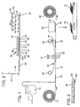
- Fig. 1 is a schematic representation of the process steps, materials, and components used to produce conductive traces on a substrate in accordance with the invention.
- Fig. 2 is a cross sectional view of a flexible film sheet having a metal layer thereon used in connection with the invention.
- Fig. 3 is an enlarged schematic representation showing the formation of a conductive trace pattern on a substrate using an adhesive-based ink composition.
- the present invention involves an improved method for producing conductive circuit traces in a highly efficient and economical manner.
- an ink composition is first used to form a selected circuit pattern on a substrate.
- a substrate 12 is illustrated.
- a wide variety of substrates known in the art may be used, including thin-film polyester, ABS (acrylonitrile-butadiene-styrene) plastic, PC (polycarbonate) plastic, PVC (polyvinyl chloride) plastic, and PC/ABS (50:50) blends.
- Other substrates may be used, and the invention shall not be limited to those listed above.
- a thermal ink jet printing system is used.
- Typical thermal ink jet systems include an ink reservoir in fluid communication with an orifice plate and resistor assembly. These types of systems are known in the art, and described in the Hewlett-Packard Journal , May 1985, Vol. 36, No. 5.
- exemplary ink jet systems with which the invention may be used are illustrated in U.S.
- Patents 4,500,895; 4,794,409; 4,791,438; 4,677,447; and 4,490,728 shall not be limited to any particular type of ink jet system, and may be implemented using a wide variety of systems known in the art, including those listed above.
- the ink jet printing apparatus 14 is designed to dispense ink in a selected circuit pattern 20 on the substrate 12 (Figs. 1 and 3.)
- the geometry of the circuit pattern 20 may be varied as desired, depending on the ultimate use for which the circuit is intended.
- the printing apparatus 14 is supplied with a specially formulated ink composition designed to adhere to the substrate 12 in a rapid and secure manner.
- a preferred adhesive usable in the invention is a product manufactured by the "Loctite Corporation of Cleveland, Ohio under the name “Loctite 408.” This material consists of a cyanoacrylate-based compound.
- Another adhesive which may be used is manufactured by Emhart Australia Pty. Ltd. of Victoria, Australia under the name “Bostik Super Bond.”
- the present invention shall not be limited to the specific adhesives described above, and other adhesives known in the art may be used accordingly.
- the adhesive is combined with one or more solvents.
- solvents include ethylene glycol phenyl ether, gamma-butyrolactone, methyl ethyl ketone, water, and mixtures thereof. But other solvents known in the art may be used.
- the solvents may be mixed in a variety of experimentally determined combinations, depending on the substrate/adhesive involved, as well as type of ink jet delivery system being used.
- the film 30 is preferably provided in a roll 32, and is more specifically illustrated in Fig. 2.
- a metal layer 40 Detachably secured to the backing layer 36 by an adhesive (not shown) is a metal layer 40 which is about 2.0 mil thick.
- the metal layer 40 may be manufactured from a wide variety of metals and alloys including but not limited to gold, copper, silver, aluminum and mixtures thereof.
- the film 30 and technical details relative thereto are specifically described in U. S. Patent 3,519,512. Also, the film 30 is commercially available from Omnicrom Systems Limited, U.K.
- the film 30 is urged downward against the pattern 20, with various portions 42 of the metal layer 40 contacting the pattern 20, as illustrated in Fig. 3. In a preferred embodiment, this step is accomplished simultaneously with the application of heat and pressure to the film 30 and pattern 20.
- An infra-red lamp, oven, or other conventional heating apparatus 41 is used to heat the film 30 to a temperature of about 20 - 250 degrees C, with a sub-range of about 50 - 70 degrees C being preferred.
- the temperature and pressure levels described above enable the adhesive in the ink to securely engage and affix the portions 42 of the metal layer 40 to the substrate 12.
- the unaffixed portions 44 of the metal layer 40 surrounding the portions 42 shown in Fig. 3 remain detached from the substrate 12.
- the film 30 is withdrawn from the substrate 12.
- the portions 42 of the metal layer 40 contacting the pattern 20 tear away from the metal layer 40 and remain adhered to the substrate 12, thus forming a metal trace pattern 50 on the substrate 12.
- the pattern 50 has a configuration identical with that of the initial pattern 20.
- the unaffixed portions 44 of the metal layer 40 remain attached to the backing layer 36 of the film 30.
- the remaining film 30 is wound onto a residue roll 55.
- the substrate 12 with the completed trace pattern 50 thereon is then cut as desired using a cutter 60 known in the art to produce individual circuit units 70 suitable for use in a wide variety of applications.
- any residual substrate 12 is preferably fed onto a collection roll 80, as illustrated in Fig. 1.
- the present invention represents a highly efficient method for applying metal trace patterns to a substrate. It is especially suitable for use in high-speed, mass production manufacturing facilities.
- the use of an ink jet system to apply an initial pattern to the substrate enables the pattern to be applied in a highly precise and controlled manner.
Landscapes
- Engineering & Computer Science (AREA)
- Manufacturing & Machinery (AREA)
- Microelectronics & Electronic Packaging (AREA)
- Mechanical Engineering (AREA)
- Manufacturing Of Printed Wiring (AREA)
Claims (8)
- Procédé d'application de traces conductrices (50) sur un substrat (12) comprenant :
la fourniture d'un substrat (12) ;
l'application d'une encre en provenance d'un système de jet d'encre sur ledit substrat (12) selon un motif (20), ladite encre comprenant un adhésif en son sein ;
le placement d'un feuille de film métallisé (30) comprenant une couche de support (36) et une couche de métal (40) qui lui est fixée de façon détachable contre ledit substrat (12) de manière à permettre à au moins une partie (42) de ladite couche de métal (40) d'entrer en contact avec ladite encre et de lui adhérer ; et
l'enlèvement dudit film (30) dudit substrat (12), ladite partie (42) de ladite couche de métal (40) qui est en contact avec ladite encre continuant à lui adhérer, certaines parties non en adhérence (44) de ladite couche de métal (40) étant ôtées dudit film (30), ladite partie (42) de ladite couche de métal (40) continuant à adhérer à ladite encre en formant un agencement de traces conductrices (50) identique audit motif (20) formé à partir de ladite encre. - Procédé selon la revendication 1, dans lequel ladite application de ladite encre sur ledit substrat (12) comprend les étapes de :
application de ladite encre à un appareil d'impression à jet d'encre thermique (14) ; et
activation dudit appareil (14) afin de délivrer ladite encre sur ledit substrat (12). - Procédé selon la revendication 1 ou 2, dans lequel ledit substrat (12) comprend un matériau choisi parmi le groupe qui comprend du polyester, du plastique d'acrylonitrile-butadiène-styrène, du plastique de chlorure de polyvinyle, du plastique de polycarbonate et des mélanges de ceux-ci.
- Procédé selon l'une quelconque des revendications 1 à 3, dans lequel ladite encre comprend environ entre 5 à 40% d'adhésif par unité de poids.
- Procédé selon l'une quelconque des revendications précédentes, dans lequel ladite couche de métal (40) comprend un métal choisi parmi le groupe qui comprend l'argent, l'or, le cuivre, l'aluminium et des mélanges de ceux-ci.
- Procédé selon l'une quelconque des revendications précédentes, dans lequel ledit placement dudit film (30) contre ledit substrat (12) comprend en outre l'étape de chauffage dudit film (30) à une température comprise entre environ 20° C et environ 250° C.
- Procédé selon la revendication 6, dans lequel ledit film (30) est poussé contre ledit substrat (12) selon une pression d'environ 30 à 50 N/cm² (3 à 5 atmosphères).
- Procédé selon l'une quelconque des revendications précédentes, dans lequel environ 3 à 20 secondes peuvent s'écouler entre ledit placement dudit film (30) contre ledit substrat (12) et ledit enlèvement dudit film (30) dudit substrat (12).
Applications Claiming Priority (2)
| Application Number | Priority Date | Filing Date | Title |
|---|---|---|---|
| US39707089A | 1989-08-22 | 1989-08-22 | |
| US397070 | 1989-08-22 |
Publications (3)
| Publication Number | Publication Date |
|---|---|
| EP0414362A2 EP0414362A2 (fr) | 1991-02-27 |
| EP0414362A3 EP0414362A3 (en) | 1991-07-17 |
| EP0414362B1 true EP0414362B1 (fr) | 1993-04-14 |
Family
ID=23569726
Family Applications (1)
| Application Number | Title | Priority Date | Filing Date |
|---|---|---|---|
| EP19900307547 Expired - Lifetime EP0414362B1 (fr) | 1989-08-22 | 1990-07-10 | Procédé pour la formation des traces conductives sur un substrat |
Country Status (5)
| Country | Link |
|---|---|
| EP (1) | EP0414362B1 (fr) |
| JP (1) | JPH0389593A (fr) |
| CA (1) | CA2014649A1 (fr) |
| DE (1) | DE69001338T2 (fr) |
| SG (1) | SG3395G (fr) |
Families Citing this family (20)
| Publication number | Priority date | Publication date | Assignee | Title |
|---|---|---|---|---|
| GB9120444D0 (en) * | 1991-09-25 | 1991-11-06 | Markem Syst Ltd | Printing apparatus and process |
| GB9408490D0 (en) * | 1994-04-27 | 1994-06-22 | Zafar Abu | Automatic foil transfer machine |
| US5800724A (en) * | 1996-02-14 | 1998-09-01 | Fort James Corporation | Patterned metal foil laminate and method for making same |
| JP3838600B2 (ja) | 1998-01-07 | 2006-10-25 | 富士写真フイルム株式会社 | 画像形成方法及び画像形成装置 |
| JP2005501761A (ja) * | 2001-09-05 | 2005-01-20 | エーピーアイ・フォイルズ・リミテッド | 金型を用いない箔押し |
| DE102005011568A1 (de) | 2004-04-13 | 2005-11-17 | Man Roland Druckmaschinen Ag | Produktionsverfahren für eine Prägeeinrichtung in einer Bogendruckmaschine |
| ES2332230T3 (es) | 2004-04-13 | 2010-01-29 | Manroland Ag | Base de apoyo para dispositivo de estampacion. |
| DE102004019412A1 (de) * | 2004-04-19 | 2005-11-03 | Man Roland Druckmaschinen Ag | Verfahren zum Drucken elektrischer und/oder elektronischer Strukturen und Folie zur Verwendung in einem solchen Verfahren |
| US8206543B2 (en) * | 2005-05-23 | 2012-06-26 | Ward Kraft | Method of manufacturing pattern coated web configurations for use in producing shaped prime labels |
| DE102005029640A1 (de) | 2005-06-25 | 2006-12-28 | Eforma | Verfahren und Vorrichtung zum Herstellen eines beliebigen Musters aus einer metallischen oder metallisierten Schicht auf einem Substrat |
| AU2006327567B2 (en) * | 2005-12-01 | 2012-12-20 | Arrow Coated Products Ltd. | Method of producing a high security film and high security film produced by the said method |
| TW200833187A (en) * | 2006-11-06 | 2008-08-01 | Basf Ag | Method for producing structured electrically conductive surfaces |
| US20080131590A1 (en) * | 2006-12-04 | 2008-06-05 | Illinois Tool Works Inc. | Method for printing electrically conductive circuits |
| DE102008033718B4 (de) | 2008-07-14 | 2021-07-29 | Bundesdruckerei Gmbh | Sicherheitsdokument mit einem Lichtleiter |
| EP2765614A1 (fr) * | 2013-02-12 | 2014-08-13 | Nederlandse Organisatie voor toegepast -natuurwetenschappelijk onderzoek TNO | Appareil rouleau à rouleau et procédé de fabrication d'un produit comprenant un substrat cible pourvu d'au moins un composant en forme de feuille |
| WO2017207829A1 (fr) * | 2016-06-01 | 2017-12-07 | DI PIETRO, Fabian Alejandro | Procédé d'obtention d'une feuille de pvc avec un aspect métallisé discontinu, feuille résultante et ses utilisations |
| EP3373712B1 (fr) | 2017-03-09 | 2023-03-29 | MGI Digital Technology | Procédé de dépôt de traces conductrices |
| US11240916B2 (en) | 2017-05-31 | 2022-02-01 | Cryovac, Llc | Electronic device, method and apparatus for producing an electronic device, and composition therefor |
| CN110217033B (zh) * | 2018-03-01 | 2021-11-26 | 东莞市图创智能制造有限公司 | 数码烫金方法及设备 |
| PL3537855T3 (pl) | 2018-03-08 | 2023-08-21 | MGI Digital Technology | Sposób wytwarzania niestandardowych bezczipowych urządzeń do identyfikacji radiowej („rfid”) |
Family Cites Families (3)
| Publication number | Priority date | Publication date | Assignee | Title |
|---|---|---|---|---|
| FR1420044A (fr) * | 1963-12-26 | 1965-12-03 | Matsushita Electric Industrial Co Ltd | Procédé de fabrication des circuits imprimés |
| US4234626A (en) * | 1978-02-01 | 1980-11-18 | E. I. Du Pont De Nemours And Company | Producing printed circuits by conjoining metal powder images |
| US4668533A (en) * | 1985-05-10 | 1987-05-26 | E. I. Du Pont De Nemours And Company | Ink jet printing of printed circuit boards |
-
1990
- 1990-04-17 CA CA 2014649 patent/CA2014649A1/fr not_active Abandoned
- 1990-07-10 EP EP19900307547 patent/EP0414362B1/fr not_active Expired - Lifetime
- 1990-07-10 DE DE1990601338 patent/DE69001338T2/de not_active Expired - Fee Related
- 1990-08-21 JP JP21988090A patent/JPH0389593A/ja active Pending
-
1995
- 1995-01-10 SG SG3395A patent/SG3395G/en unknown
Also Published As
| Publication number | Publication date |
|---|---|
| CA2014649A1 (fr) | 1991-02-22 |
| SG3395G (en) | 1995-06-16 |
| EP0414362A2 (fr) | 1991-02-27 |
| JPH0389593A (ja) | 1991-04-15 |
| EP0414362A3 (en) | 1991-07-17 |
| DE69001338D1 (de) | 1993-05-19 |
| DE69001338T2 (de) | 1993-11-18 |
Similar Documents
| Publication | Publication Date | Title |
|---|---|---|
| EP0414362A2 (fr) | Procédé pour la formation des traces conductives sur un substrat | |
| US5114744A (en) | Method for applying a conductive trace pattern to a substrate | |
| EP0414363B1 (fr) | Procédé d'application d'un patron de traces conductrices sur un substrat | |
| US5882722A (en) | Electrical conductors formed from mixtures of metal powders and metallo-organic decompositions compounds | |
| US4221925A (en) | Printed circuit board | |
| US5721007A (en) | Process for low density additive flexible circuits and harnesses | |
| EP0117258B1 (fr) | Procédés pour réaliser des couches métalliques adhérentes à des supports en matière synthétique | |
| JPS6140316A (ja) | 直接はんだ付け可能な導電性組成物 | |
| CA2305696A1 (fr) | Fabrication d'objets metalliques minces | |
| JP5843992B1 (ja) | 無電解めっき用転写フィルム用触媒組成物及び無電解めっき用転写フィルム | |
| JP2012210715A (ja) | 金属箔の転写方法 | |
| EP0834898A3 (fr) | Panneau de blindage électromagnétique et son procédé de fabrication | |
| JPS5848988A (ja) | 印刷配線板の製造方法 | |
| EP0148601A2 (fr) | Laminage par transfert de motifs électriquement conducteurs | |
| US6981318B2 (en) | Printed circuit board manufacturing method | |
| US20070295448A1 (en) | System for forming leaf laminates | |
| US3218214A (en) | Thermoplastic shrink inhibitor | |
| JP6612419B1 (ja) | 無電解めっき用真空転写フィルム | |
| US3998677A (en) | Technique for using solder etch resist in generation of patterns on printed wiring boards | |
| GB2047971A (en) | Printed circuit fabrication | |
| KR20010070561A (ko) | 입체문양용 용해 열전사지 및 그 제조방법 | |
| JPS63284886A (ja) | 金属パタ−ン形成方法 | |
| JPS62122295A (ja) | 高導電性電気回路及びその製造方法 | |
| JPS5815952B2 (ja) | 接着剤被覆積層板の製造法 | |
| JPS63282280A (ja) | パタ−ン形成方法 |
Legal Events
| Date | Code | Title | Description |
|---|---|---|---|
| PUAI | Public reference made under article 153(3) epc to a published international application that has entered the european phase |
Free format text: ORIGINAL CODE: 0009012 |
|
| AK | Designated contracting states |
Kind code of ref document: A2 Designated state(s): DE FR GB IT |
|
| PUAL | Search report despatched |
Free format text: ORIGINAL CODE: 0009013 |
|
| AK | Designated contracting states |
Kind code of ref document: A3 Designated state(s): DE FR GB IT |
|
| 17P | Request for examination filed |
Effective date: 19911223 |
|
| 17Q | First examination report despatched |
Effective date: 19920612 |
|
| GRAA | (expected) grant |
Free format text: ORIGINAL CODE: 0009210 |
|
| AK | Designated contracting states |
Kind code of ref document: B1 Designated state(s): DE FR GB IT |
|
| REF | Corresponds to: |
Ref document number: 69001338 Country of ref document: DE Date of ref document: 19930519 |
|
| ET | Fr: translation filed | ||
| ITF | It: translation for a ep patent filed | ||
| PLBE | No opposition filed within time limit |
Free format text: ORIGINAL CODE: 0009261 |
|
| STAA | Information on the status of an ep patent application or granted ep patent |
Free format text: STATUS: NO OPPOSITION FILED WITHIN TIME LIMIT |
|
| 26N | No opposition filed | ||
| REG | Reference to a national code |
Ref country code: GB Ref legal event code: 732E |
|
| REG | Reference to a national code |
Ref country code: FR Ref legal event code: TP |
|
| REG | Reference to a national code |
Ref country code: GB Ref legal event code: IF02 |
|
| PGFP | Annual fee paid to national office [announced via postgrant information from national office to epo] |
Ref country code: GB Payment date: 20050706 Year of fee payment: 16 |
|
| PGFP | Annual fee paid to national office [announced via postgrant information from national office to epo] |
Ref country code: FR Payment date: 20050718 Year of fee payment: 16 |
|
| PGFP | Annual fee paid to national office [announced via postgrant information from national office to epo] |
Ref country code: DE Payment date: 20050831 Year of fee payment: 16 |
|
| PG25 | Lapsed in a contracting state [announced via postgrant information from national office to epo] |
Ref country code: GB Free format text: LAPSE BECAUSE OF NON-PAYMENT OF DUE FEES Effective date: 20060710 |
|
| PGFP | Annual fee paid to national office [announced via postgrant information from national office to epo] |
Ref country code: IT Payment date: 20060731 Year of fee payment: 17 |
|
| PG25 | Lapsed in a contracting state [announced via postgrant information from national office to epo] |
Ref country code: DE Free format text: LAPSE BECAUSE OF NON-PAYMENT OF DUE FEES Effective date: 20070201 |
|
| GBPC | Gb: european patent ceased through non-payment of renewal fee |
Effective date: 20060710 |
|
| REG | Reference to a national code |
Ref country code: FR Ref legal event code: ST Effective date: 20070330 |
|
| PG25 | Lapsed in a contracting state [announced via postgrant information from national office to epo] |
Ref country code: FR Free format text: LAPSE BECAUSE OF NON-PAYMENT OF DUE FEES Effective date: 20060731 |
|
| PG25 | Lapsed in a contracting state [announced via postgrant information from national office to epo] |
Ref country code: IT Free format text: LAPSE BECAUSE OF NON-PAYMENT OF DUE FEES Effective date: 20070710 |