EP0414647A2 - Verfahren zum Herstellen eines Leitergitters - Google Patents
Verfahren zum Herstellen eines Leitergitters Download PDFInfo
- Publication number
- EP0414647A2 EP0414647A2 EP90830313A EP90830313A EP0414647A2 EP 0414647 A2 EP0414647 A2 EP 0414647A2 EP 90830313 A EP90830313 A EP 90830313A EP 90830313 A EP90830313 A EP 90830313A EP 0414647 A2 EP0414647 A2 EP 0414647A2
- Authority
- EP
- European Patent Office
- Prior art keywords
- pins
- bending
- punch
- die
- metal frame
- Prior art date
- Legal status (The legal status is an assumption and is not a legal conclusion. Google has not performed a legal analysis and makes no representation as to the accuracy of the status listed.)
- Withdrawn
Links
Images
Classifications
-
- H—ELECTRICITY
- H10—SEMICONDUCTOR DEVICES; ELECTRIC SOLID-STATE DEVICES NOT OTHERWISE PROVIDED FOR
- H10W—GENERIC PACKAGES, INTERCONNECTIONS, CONNECTORS OR OTHER CONSTRUCTIONAL DETAILS OF DEVICES COVERED BY CLASS H10
- H10W70/00—Package substrates; Interposers; Redistribution layers [RDL]
- H10W70/40—Leadframes
- H10W70/421—Shapes or dispositions
- H10W70/424—Cross-sectional shapes
-
- H—ELECTRICITY
- H10—SEMICONDUCTOR DEVICES; ELECTRIC SOLID-STATE DEVICES NOT OTHERWISE PROVIDED FOR
- H10W—GENERIC PACKAGES, INTERCONNECTIONS, CONNECTORS OR OTHER CONSTRUCTIONAL DETAILS OF DEVICES COVERED BY CLASS H10
- H10W70/00—Package substrates; Interposers; Redistribution layers [RDL]
- H10W70/01—Manufacture or treatment
- H10W70/04—Manufacture or treatment of leadframes
- H10W70/048—Mechanical treatments, e.g. punching, cutting, deforming or cold welding
-
- Y—GENERAL TAGGING OF NEW TECHNOLOGICAL DEVELOPMENTS; GENERAL TAGGING OF CROSS-SECTIONAL TECHNOLOGIES SPANNING OVER SEVERAL SECTIONS OF THE IPC; TECHNICAL SUBJECTS COVERED BY FORMER USPC CROSS-REFERENCE ART COLLECTIONS [XRACs] AND DIGESTS
- Y10—TECHNICAL SUBJECTS COVERED BY FORMER USPC
- Y10T—TECHNICAL SUBJECTS COVERED BY FORMER US CLASSIFICATION
- Y10T29/00—Metal working
- Y10T29/49—Method of mechanical manufacture
- Y10T29/49002—Electrical device making
- Y10T29/49117—Conductor or circuit manufacturing
- Y10T29/49204—Contact or terminal manufacturing
- Y10T29/49208—Contact or terminal manufacturing by assembling plural parts
- Y10T29/49218—Contact or terminal manufacturing by assembling plural parts with deforming
-
- Y—GENERAL TAGGING OF NEW TECHNOLOGICAL DEVELOPMENTS; GENERAL TAGGING OF CROSS-SECTIONAL TECHNOLOGIES SPANNING OVER SEVERAL SECTIONS OF THE IPC; TECHNICAL SUBJECTS COVERED BY FORMER USPC CROSS-REFERENCE ART COLLECTIONS [XRACs] AND DIGESTS
- Y10—TECHNICAL SUBJECTS COVERED BY FORMER USPC
- Y10T—TECHNICAL SUBJECTS COVERED BY FORMER US CLASSIFICATION
- Y10T29/00—Metal working
- Y10T29/51—Plural diverse manufacturing apparatus including means for metal shaping or assembling
- Y10T29/5193—Electrical connector or terminal
Definitions
- the present invention relates to the fabrication of Single-In-Line semiconductor devices, especially in a molded plastic package.
- SIL Single-In-Line
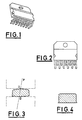
- the defect which may be easily observed in Fig. 2 is induced by the fact that the cross section of the various pins which are patterned by die stamping a strip of copper or nickel plated copper sheet from which the assembly metal frame of the semiconductor device is made, may present abutment lines of the bending punch and of the contrasting punch which are offset among each other. This is shown in Fig. 3 by joining these abutment lines with an imaginary secant plane identified by the dash-point line T.
- the bending punch abuts on the highest point U of the cross section while the contrasting punch exerts its restraining action on the point V (at least at the beginning of the bending).
- This offset between the pressure points creates a torque which induces a torsion on the pin which in turn determines the assumption of a slight lateral slanting thereof. This causes an effect such as the one depicted in Fig. 2 on the finished article.
- the bending punches of the pins upon completion of the assembly will act on pin surfaces which are essentially parallel to each other and the bending will no longer induce a torsion and a consequent lateral slanting as it occurs with unstriken pins having a cross section so as resulting from the die stamping, as schematically shown in Fig. 3.
- plastic deformation induced by the press striking step in the selected outer region of the die stamped metal frame should not exceed a certain limit in order to avoid to excessively work-harden the metal which must later be bent.
Landscapes
- Bending Of Plates, Rods, And Pipes (AREA)
Applications Claiming Priority (2)
| Application Number | Priority Date | Filing Date | Title |
|---|---|---|---|
| IT8363189 | 1989-07-18 | ||
| IT8983631A IT1235832B (it) | 1989-07-18 | 1989-07-18 | Coniatura dei telai tranciati per ripristinare il parallelismo delle superfici dei piedini in vista della loro piegatura definitiva in contenitori single in line. |
Publications (2)
| Publication Number | Publication Date |
|---|---|
| EP0414647A2 true EP0414647A2 (de) | 1991-02-27 |
| EP0414647A3 EP0414647A3 (en) | 1991-06-05 |
Family
ID=11323411
Family Applications (1)
| Application Number | Title | Priority Date | Filing Date |
|---|---|---|---|
| EP19900830313 Withdrawn EP0414647A3 (en) | 1989-07-18 | 1990-07-06 | Method for the fabrication of a lead frame |
Country Status (3)
| Country | Link |
|---|---|
| US (1) | US5075941A (de) |
| EP (1) | EP0414647A3 (de) |
| IT (1) | IT1235832B (de) |
Cited By (6)
| Publication number | Priority date | Publication date | Assignee | Title |
|---|---|---|---|---|
| GB2417221A (en) * | 2004-08-20 | 2006-02-22 | Glenn Brazier | A device for re-positioning the legs of semi conductors whilst they are still in their packaging |
| CN104190817A (zh) * | 2014-09-02 | 2014-12-10 | 中江县凯讯电子有限公司 | 一种网络变压器引脚弯折设备 |
| CN104190820A (zh) * | 2014-09-02 | 2014-12-10 | 中江县凯讯电子有限公司 | 便于控制变形量的网络变压器引脚弯折机构 |
| CN104190816A (zh) * | 2014-09-02 | 2014-12-10 | 中江县凯讯电子有限公司 | 弯折量便于控制的引脚弯折机构 |
| CN104190819A (zh) * | 2014-09-02 | 2014-12-10 | 中江县凯讯电子有限公司 | 网络变压器加工装置 |
| CN104209427A (zh) * | 2014-09-02 | 2014-12-17 | 中江县凯讯电子有限公司 | 一种引脚弯折设备 |
Families Citing this family (3)
| Publication number | Priority date | Publication date | Assignee | Title |
|---|---|---|---|---|
| JP2837064B2 (ja) * | 1993-05-25 | 1998-12-14 | ローム株式会社 | ボンディングパッド面の圧印加工方法 |
| CN104190818B (zh) * | 2014-09-02 | 2016-03-02 | 中江县凯讯电子有限公司 | 用于引脚宽度弯折且弯折量便于控制的机构 |
| WO2021012575A1 (zh) * | 2019-07-19 | 2021-01-28 | 苏州光越微纳科技有限公司 | 一种用于电子元件的折弯模具 |
Family Cites Families (6)
| Publication number | Priority date | Publication date | Assignee | Title |
|---|---|---|---|---|
| FR1084037A (fr) * | 1952-09-27 | 1955-01-14 | Philips Nv | Procédé de suppression des bavures des pièces découpées |
| US4205548A (en) * | 1978-07-03 | 1980-06-03 | Plessey, Inc. | Stamping tools |
| US4553420A (en) * | 1983-09-30 | 1985-11-19 | Asm Fico Tooling, B.V. | Method and apparatus for touch-free lead bending |
| JPS60235110A (ja) * | 1984-05-07 | 1985-11-21 | Minolta Camera Co Ltd | 焦点検出装置の温度補償装置 |
| JPS62275525A (ja) * | 1986-05-21 | 1987-11-30 | Hitachi Ltd | リ−ドフレ−ム曲げ型 |
| JPS63129652A (ja) * | 1986-11-20 | 1988-06-02 | Toshiba Corp | 半導体装置 |
-
1989
- 1989-07-18 IT IT8983631A patent/IT1235832B/it active
-
1990
- 1990-07-06 EP EP19900830313 patent/EP0414647A3/en not_active Withdrawn
- 1990-07-17 US US07/553,331 patent/US5075941A/en not_active Expired - Lifetime
Cited By (10)
| Publication number | Priority date | Publication date | Assignee | Title |
|---|---|---|---|---|
| GB2417221A (en) * | 2004-08-20 | 2006-02-22 | Glenn Brazier | A device for re-positioning the legs of semi conductors whilst they are still in their packaging |
| CN104190817A (zh) * | 2014-09-02 | 2014-12-10 | 中江县凯讯电子有限公司 | 一种网络变压器引脚弯折设备 |
| CN104190820A (zh) * | 2014-09-02 | 2014-12-10 | 中江县凯讯电子有限公司 | 便于控制变形量的网络变压器引脚弯折机构 |
| CN104190816A (zh) * | 2014-09-02 | 2014-12-10 | 中江县凯讯电子有限公司 | 弯折量便于控制的引脚弯折机构 |
| CN104190819A (zh) * | 2014-09-02 | 2014-12-10 | 中江县凯讯电子有限公司 | 网络变压器加工装置 |
| CN104209427A (zh) * | 2014-09-02 | 2014-12-17 | 中江县凯讯电子有限公司 | 一种引脚弯折设备 |
| CN104209427B (zh) * | 2014-09-02 | 2016-03-02 | 中江县凯讯电子有限公司 | 一种引脚弯折设备 |
| CN104190819B (zh) * | 2014-09-02 | 2016-03-02 | 中江县凯讯电子有限公司 | 网络变压器加工装置 |
| CN104190816B (zh) * | 2014-09-02 | 2016-03-02 | 中江县凯讯电子有限公司 | 弯折量便于控制的引脚弯折机构 |
| CN104190820B (zh) * | 2014-09-02 | 2016-03-02 | 中江县凯讯电子有限公司 | 便于控制变形量的网络变压器引脚弯折机构 |
Also Published As
| Publication number | Publication date |
|---|---|
| IT1235832B (it) | 1992-11-03 |
| EP0414647A3 (en) | 1991-06-05 |
| IT8983631A0 (it) | 1989-07-18 |
| US5075941A (en) | 1991-12-31 |
Similar Documents
| Publication | Publication Date | Title |
|---|---|---|
| US5075941A (en) | Press striking of die stamped metal frames for single-in-line packages for re-establishing planarity and parallellism of the opposite faces of the patterned pins to be eventually bent | |
| US5696029A (en) | Process for manufacturing a lead frame | |
| US5495780A (en) | Method for sharpening an IC lead-frame punch | |
| US5521430A (en) | Semiconductor apparatus and its manufacturing method | |
| JP4903205B2 (ja) | フリップチップ・パッケージングされた半導体デバイス及び半導体ダイをパッケージングする方法 | |
| JP2752558B2 (ja) | 電子部品の製造方法 | |
| JP2617218B2 (ja) | 半導体部品の製造方法及びその製造方法に使用するリードフレーム | |
| US5293064A (en) | Lead frame and method of manufacturing a semiconductor device | |
| JPH08148623A (ja) | 半導体装置 | |
| JP2752556B2 (ja) | 電子部品の製造方法 | |
| US6928850B2 (en) | Method and tooling for z-axis offset of lead frames | |
| JPH0730042A (ja) | 半導体装置用リードフレーム、それを用いた半導体装置及びその製造方法 | |
| JP3744756B2 (ja) | リードフレームの製造方法 | |
| JPH05190748A (ja) | 電子部品の実装パッケージ製造方法 | |
| JPH05144988A (ja) | 半導体装置の製造方法並びに半導体製造装置及びリードフレーム | |
| JP2555989B2 (ja) | 樹脂封止型半導体装置およびリードフレーム | |
| JPH0325418Y2 (de) | ||
| JP4073198B2 (ja) | 半導体装置及び半導体装置の製造方法 | |
| JP2708343B2 (ja) | 半導体装置の製造方法およびリードフレーム | |
| JPH04229642A (ja) | 電子部品の製造方法及びその製造に使用するリードフレームの構造 | |
| JPH03152965A (ja) | リードフレーム及び半導体装置の製造方法 | |
| JPH0430186B2 (de) | ||
| JPH07176671A (ja) | リードフレームおよびその製造方法 | |
| JPH0744249B2 (ja) | 電子部品のリード加工方法 | |
| KR200160429Y1 (ko) | 리드프레임 패드 챔퍼용 금형 |
Legal Events
| Date | Code | Title | Description |
|---|---|---|---|
| PUAI | Public reference made under article 153(3) epc to a published international application that has entered the european phase |
Free format text: ORIGINAL CODE: 0009012 |
|
| AK | Designated contracting states |
Kind code of ref document: A2 Designated state(s): DE FR GB NL SE |
|
| PUAL | Search report despatched |
Free format text: ORIGINAL CODE: 0009013 |
|
| AK | Designated contracting states |
Kind code of ref document: A3 Designated state(s): DE FR GB NL SE |
|
| 17P | Request for examination filed |
Effective date: 19911021 |
|
| 17Q | First examination report despatched |
Effective date: 19930507 |
|
| RAP3 | Party data changed (applicant data changed or rights of an application transferred) |
Owner name: STMICROELECTRONICS S.R.L. |
|
| APAD | Appeal reference recorded |
Free format text: ORIGINAL CODE: EPIDOS REFNE |
|
| APCB | Communication from the board of appeal sent |
Free format text: ORIGINAL CODE: EPIDOS OBAPE |
|
| APCB | Communication from the board of appeal sent |
Free format text: ORIGINAL CODE: EPIDOS OBAPE |
|
| APAB | Appeal dossier modified |
Free format text: ORIGINAL CODE: EPIDOS NOAPE |
|
| GRAG | Despatch of communication of intention to grant |
Free format text: ORIGINAL CODE: EPIDOS AGRA |
|
| GRAG | Despatch of communication of intention to grant |
Free format text: ORIGINAL CODE: EPIDOS AGRA |
|
| GRAH | Despatch of communication of intention to grant a patent |
Free format text: ORIGINAL CODE: EPIDOS IGRA |
|
| STAA | Information on the status of an ep patent application or granted ep patent |
Free format text: STATUS: THE APPLICATION HAS BEEN WITHDRAWN |
|
| 18W | Application withdrawn |
Withdrawal date: 20010714 |
|
| APAF | Appeal reference modified |
Free format text: ORIGINAL CODE: EPIDOSCREFNE |