EP0415751A1 - Condensateur à couche mince et son procédé de fabrication - Google Patents
Condensateur à couche mince et son procédé de fabrication Download PDFInfo
- Publication number
- EP0415751A1 EP0415751A1 EP90309478A EP90309478A EP0415751A1 EP 0415751 A1 EP0415751 A1 EP 0415751A1 EP 90309478 A EP90309478 A EP 90309478A EP 90309478 A EP90309478 A EP 90309478A EP 0415751 A1 EP0415751 A1 EP 0415751A1
- Authority
- EP
- European Patent Office
- Prior art keywords
- film
- oxide
- silicide
- electrode layer
- silicon
- Prior art date
- Legal status (The legal status is an assumption and is not a legal conclusion. Google has not performed a legal analysis and makes no representation as to the accuracy of the status listed.)
- Granted
Links
Images


Classifications
-
- H—ELECTRICITY
- H10—SEMICONDUCTOR DEVICES; ELECTRIC SOLID-STATE DEVICES NOT OTHERWISE PROVIDED FOR
- H10B—ELECTRONIC MEMORY DEVICES
- H10B53/00—Ferroelectric RAM [FeRAM] devices comprising ferroelectric memory capacitors
-
- H—ELECTRICITY
- H10—SEMICONDUCTOR DEVICES; ELECTRIC SOLID-STATE DEVICES NOT OTHERWISE PROVIDED FOR
- H10D—INORGANIC ELECTRIC SEMICONDUCTOR DEVICES
- H10D1/00—Resistors, capacitors or inductors
- H10D1/60—Capacitors
- H10D1/68—Capacitors having no potential barriers
-
- Y—GENERAL TAGGING OF NEW TECHNOLOGICAL DEVELOPMENTS; GENERAL TAGGING OF CROSS-SECTIONAL TECHNOLOGIES SPANNING OVER SEVERAL SECTIONS OF THE IPC; TECHNICAL SUBJECTS COVERED BY FORMER USPC CROSS-REFERENCE ART COLLECTIONS [XRACs] AND DIGESTS
- Y10—TECHNICAL SUBJECTS COVERED BY FORMER USPC
- Y10T—TECHNICAL SUBJECTS COVERED BY FORMER US CLASSIFICATION
- Y10T29/00—Metal working
- Y10T29/43—Electric condenser making
- Y10T29/435—Solid dielectric type
Definitions
- the present invention relates to a thin film capacitor and a manufacturing method thereof, and more particularly to a thin film capacitor used for ICs and LSIs and a manufacturing method thereof.
- the electronic circuits are being miniaturized to an increasing degree as a result of advances in the integrated circuit technologies, and the miniaturization of capacitors that are indispensable in the integrated circuits as circuit elements for various kinds of electronic circuits is also becoming especially significant.
- the miniaturization of thin film capacitors is being delayed in the midst of a rapid progress in the miniaturization of the active elements, which is becoming a substantial factor as an obstruction for a further enhancement in the integration.
- the reason for this is that the dielectric thin films are limited to those materials such as SiO2, Si3N4 and the like that have dielectric constant of less than 10. Therefore, it is becoming necessary to develop dielectric thin films having a large dielectric constant as a means of the miniaturization of thin film capacitors.
- BaTiO3, SrTiO3 and PbZrO3 which are perovskite type oxides and an ilmenite type oxide LiNbO3 that are represented by the chemical formula ABO3, or oxides belonging to ferroelectric materials such as Bi4Ti3O12, have dielectric constant of larger than 100 and reaching even to 10000 in the form of a single crystal or a ceramic as the above-mentioned single composition and the mutual solid solution composition, and these oxides are being used widely for ceramic capacitors.
- To make these materials into thin films is extremely effective for the miniaturization of the above-mentioned thin film capacitors, and it has been studied since fairly long time ago.
- Dielectric thin films such as the above-mentioned BaTiO3, that have been formed in the past require high temperatures at the time of thin film formation in order to obtain high dielectric constants, being formed without exception on a lower electrode of a high-melting point noble metal such as platinum and palladium.
- a high-melting point noble metal such as platinum and palladium.
- the electrode material used extensively for the present day highly integrated circuits is polycrystalline silicon or a low resistance silicon layer with impurities doped to a high concentration in a portion of the silicon substrate itself.
- silicon electrodes the fine processing technologies have been established and have already been used extensively. Therefore, if a thin film with satisfactory high dielectric constant can be prepared on a silicon electrode, it becomes possible to apply the technology to capacitors for integrated circuits.
- a means of further employing a platinum or palladium electrode between the high dielectric constant material film and the silicon electrode also in the case of using a silicon electrode as the lower electrode The structure for this case is shown in Fig. 1.
- Reference numeral 11 is a silicon substrate
- 12 is a low-resistance silicon electrode layer doped with a high concentration impurity such as phosphorus or arsenic
- 13 is an insulating layer of such material as SiO2
- 14 is a platinum electrode layer
- 15 is a dielectric layer
- 16 is an upper electrode layer of such material as aluminum
- 17 is a lead-out wiring for the lower electrode.
- the formation of the high dielectric constant material film represented by BaTiO3 and SrTiO3 has to be done at high temperatures as mentioned above. Accordingly, with the means shown in Fig. 1, the platinum layer 14 reacts with the silicon electrode 12 forming platinum silicide, and further, there is formed an SiO2 layer on its interface with the dielectric layer 15, and as a result, the effective dielectric constant is markedly reduced analogous to the case of the silicon electrode described in the above.
- a thin film capacitor which comprises a silicon electrode, a first electrode layer formed on the silicon electrode, and consisting essentially of a member selected from the group consisting of titanium, titanium silicide, titanium nitride, tantalum, molybdenum, tungsten, tantalum silicide, molybdenum silicide, tungsten silicide, alloys thereof and compounds thereof, a second electrode layer consisting essentially of a high-melting point noble metal formed on the first electrode layer, a dielectric layer consisting essentially of an oxide ferroelectric material formed on the second electrode layer and a third electrode layer formed on the dielectric layer.
- a manufacturing method of a thin film capacitor that includes the steps of forming on a silicon electrode a first electrode layer consisting essentially of a member selected from the group consisting of titanium, titanium silicide, titanium nitride, tantalum, molybdenum, tungsten, tantalum silicide, molybdenum silicide, tungsten silicide, alloys thereof and compounds thereof, forming a second electrode layer consisting essentially of a high-melting point noble metal on the first electrode layer, forming a dielectric layer consisting essentially of an oxide ferroelectric material on the second electrode layer and forming a third electrode layer on the dielectric layer.
- a thin film capacitor which comprises a silicon electrode, a first electrode layer formed on the silicon electrode, the first electrode layer being formed essentially of a member selected from the group of rhenium oxide, osmium oxide, rhodium oxide, iridium oxide and compounds thereof, a second electrode layer consisting essentially of a high-melting point noble metal formed on the first electrode layer, a dielectric layer consisting essentially of an oxide ferroelectric material formed on the second electrode layer and a third electrode layer formed on the dielectric layer.
- a manufacturing method of a thin film capacitor that includes the steps of forming on a silicon electrode a first electrode layer consisting essentially of a member selected from the group of rhenium oxide, osmium oxide, rhodium oxide, iridium oxide and compounds thereof, forming a second electrode layer consisting essentially of a high-melting point noble metal on the first electrode layer, forming a dielectric layer consisting essentially of an oxide ferroelectric material on the second electrode layer and forming a third electrode layer on the dielectric layer.
- a method of manufacturing a thin film capacitor that includes the steps of forming on a silicon electrode a first electrode layer consisting essentially of a member selected from the group of rhenium silicide, osmium silicide, rhodium silicide, iridium silicide and compounds thereof, oxidizing the first electrode layer at 400 to 700°C, forming a second electrode layer consisting essentially of a high-melting point noble metal on the oxidized first electrode layer, forming a dielectric layer consisting essentially of an oxide ferroelectric material on the second electrode layer and forming a third electrode layer on the dielectric layer.
- a polycrystalline silicon layer or a silicon single crystal layer or a substrate doped with an impurity may be preferably employed.
- platinum, palladium, rhodium or alloys thereof may be preferably used therefor.
- a perovskite type oxide, an ilmenite type oxide or Bi4Ti3O12 may be preferably employed.
- the perovskite type oxides BaTiO3, SrTiO3, PbTiO3, PbZrO3 and the solid solutions thereof may be preferably used and as the ilmenite type oxides, LiNbO3, LiTaO3 and the solid solution thereof may be preferably used.
- the third electrode preferable use is made of aluminum.
- 21 is a silicon substrate
- 22 is a low resistance silicon electrode layer doped with impurities to a high concentration
- 24 is an intermediate layer having a thickness from 500 ⁇ to 1500 ⁇ and consisting of a material selected from the group of titanium, titanium silicide and titanium nitride or a laminated layer thereof, is a platinum electrode layer
- 26 is a dielectric layer
- 27 is an upper electrode layer made of aluminum or the like
- 28 is a lower electrode lead-out layer made of aluminum or the like.
- the BaTiO3 film is prepared by a high frequency magnetron sputtering that uses a target with stoichiometric composition.
- the film is formed in a mixed gas of argon and oxygen under a pressure of 1 x 10 ⁇ 2 Torr and a substrate temperature of 400 to 500°C.
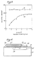
- the curve 31 shows the measured values for a sample with the configuration as shown in Fig. 2.
- the effective dielectric constant is seen to have a constant value of about 240 which is independent of the thickness of the BaTiO3 film, showing that there are not formed layers of low dielectric constant at the interface. This characteristic is seen to be obtained for either case of using titanium, titanium silicide and titanium nitride as the intermediate layer 24.
- the same characteristic is also observed when a laminated intermediate layer titanium/titanium silicide, for example, is used.
- the intermediate layer can be formed by a magnetron sputtering method by selecting either one from titanium, titanium silicide and titanium nitride as the target and adjusting the atmosphere appropriately.
- the curve 32 in Fig. 3 shows the result of measurement on a sample with the configuration shown in Fig. 1 for the purpose of comparison. In this case the effective dielectric constant goes down with the reduction in the thickness of the BaTiO3 film, indicating clearly that there are generated layers of low dielectric constant at the interface.
- FIG. 4 Another embodiment of the present invention is shown in Fig. 4.
- Reference numerals 21 to 28 are the same as in Fig. 2 and 29 is a low resistance polycrystalline silicon layer.
- the present embodiment uses flat layers of electrodes and dielectric material and is realized by forming a low resistance polycrystalline silicon layer 29 in a contact opening part formed in the insulating layer 23, then forming an intermediate layer 24 and a platinum layer 25.
- a low resistance layer 52 is formed by doping phosphorus to a high concentration in a part of the surface of single crystal silicon 51, and, a silicon oxide film 53 is formed on top of it as an interlayer insulating film.
- a couple of contact holes are formed in parts of the silicon oxide film 53 for leading out the lower electrode through the low resistance layer 52, one of the contact holes is filled with a polycrystalline silicon film 54 while the other contact hole is filled with an aluminum film 55. Accordingly, the aluminum film 55 will serve as a terminal of the lower electrode.
- the lower electrode film 54 not only fills the contact hole but also part of it may be formed on the silicon oxide film 53.
- a BaTiO3 film 56 is formed on the lower electrode film 54, and an aluminum film 57 is formed on top of it as an upper electrode.
- a multilayered film of platinum and titanium of the conductive layer for the present embodiment are prepared by a dc magnetron sputtering in an argon atmosphere under a pressure of 4 x 10 ⁇ 3 Torr and a substrate temperature of 100°C to the thicknesses of 3000 and 500 ⁇ , respectively.
- the BaTiO3 film 56 with thickness of 5000 ⁇ is prepared by a high frequency magnetron sputtering using a powder target of stoichiometric composition.
- the film is formed in a mixed gas of argon and oxygen under a pressure of 1 x 10 ⁇ 2 Torr and a substrate temperature of 600°C.
- An aluminum film of 5000 ⁇ is formed as the upper electrode by a dc sputtering.
- the effective area of the present capacitor is 250 ⁇ m2.
- the differences in the characteristics of the BaTiO3 film for the case of using the multilayered film of platinum and titanium of the present embodiment and the case of using only a platinum film which is a high melting point noble metal as the conductive layer, and the case of forming no conductive layer are shown in Figs. 6(a), 6(b) and 6(c), respectively.
- the dielectric constant of the BaTiO3 film is reduced markedly with the decrease in the thickness of the dielectric film for the cases of using the platinum film and the polycrystalline film.
- the fall of the dielectric constant in the case of the polycrystalline silicon film is caused by the formation of a layer of low dielectric constant due to oxidation of silicon at the interface between the dielectric film and the electrode as has been reported in the past.
- the drop in the dielectric constant in the case of the platinum film is due to the formation of the silicide compound of platinum. Namely, silicon reacts with platinum during the formation of the dielectric film at 600°C, and reaches the uppermost surface while forming the silicide compound. It is considered that silicon that reached the uppermost surface is oxidized to form a layer of low dielectric constant similar to the case of the polycrystalline silicon film. It is confirmed by X-ray diffraction that silicidation of platinum occurred after the formation of the dielectric film.
- the materials used for the present embodiment are summarized in Table 1.
- Table 1 1 Alloy Film Mo 20at% - Ti 80at%, 500 ⁇ 2 Alloy Film W 20at% - Mo 80at%, 500 ⁇ 3 Alloy Film Ta 50at% - Ti 50at%, 500 ⁇ 4 Alloy Film TaSi 50at% - TiSi 50at%, 500 ⁇ 5 Multilayered Film Mo(300 ⁇ )/Ti(200 ⁇ ) 6 Multilayered Film W(300 ⁇ )/Mo(200 ⁇ ) 7 Multilayered Film Ta(300 ⁇ )/Ti(200 ⁇ ) 8 Multilayered Film TaSi(300 ⁇ )/TiSi(200 ⁇ )
- the dielectric constant of the BaTiO3 film maintained its intrinsic value without having dependence on the film thickness, and was possible to prevent the formation at the interface of a layer with low dielectric constant, analogous to the third embodiment. Moreover, it was confirmed by X-ray diffraction that silicidation of platinum of the second layer dose not occur.
- the materials used in the present embodiment are listed in Table 2.
- Table 2 1 Alloy Film Pt 85at% - Rh 15at%, 1500 ⁇ 2 Alloy Film Pt 80at% - Pd 20at%, 1500 ⁇ 3 Alloy Film Pd 90at% - Rh 10at%, 1500 ⁇ 4 Multilayered Film Pt(1000 ⁇ )/Rh(500 ⁇ ) 5 Multilayered Film Pt(1000 ⁇ )/Pd(500 ⁇ ) 6 Multilayered Film Pd(1000 ⁇ )/Rh(500 ⁇ )
- a low resistance layer 72 with highly doped phosphorus is formed in a part of the surface of single crystal silicon 71, and a silicon oxide film 73 is formed on top of it as an interlayer insulating film.
- Two contact holes for leading out the lower electrode through the low resistance layer are formed in parts of the silicon oxide film 73, one of the contact holes is filled with a polycrystalline silicon film 74 while the other contact hole is filled with an aluminum film 75. Accordingly, the aluminum film 75 will be served as the terminal of the lower electrode.
- the lower electrode film 74 fills the contact hole, and a part of it may be formed on the silicon oxide film 73.
- a first layer 76 and a second layer 77 of a conductive layer are formed, a BaTiO3 film 78 is formed on it, and an aluminum film 79 is further formed on top of it as an upper electrode.
- the first layer 76 of rhenium oxide and the second layer of platinum of the conductive layer are formed sequentially by a dc magnetron sputtering method using an ReO3 and a Pt targets, respectively.
- the film formation is carried out in an atmosphere of argon gas under a pressure of 4 x 10 ⁇ 3 Torr and a substrate temperature of 100°C, with the thicknesses of both of platinum and rhenium oxide set at 1500 ⁇ .
- the BaTiO3 film 78 is prepared by a high frequency magnetron sputtering to a thickness of 3000 ⁇ using a powder target of stoichiometric composition in a mixed gas of argon and oxygen under a pressure of 1 x 10 ⁇ 2 Torr and a substrate temperature of 600°C.
- the upper electrode is formed as an aluminum film with thickness of 5000 ⁇ by a dc sputtering method.
- the effective area of the present capacitor is 250 ⁇ m2.
- the dielectric constant of the dielectric film for the case of using the platinum film and the polycrystalline silicon film is reduced markedly with a decrease in the film thickness.
- the drop of the dielectric constant for the case the polycrystalline silicon film is due to the formation of an oxide layer of silicon at the interface of the dielectric film and the electrode or the formation of a layer of low dielectric constant in the initial period of growth of a dielectric film, as has been reported in the past.
- the platinum film of Fig. 8(b) it is confirmed by X-ray diffraction after the formation of the dielectric film that silicidation of platinum occurred. This means that silicon reacted with platinum during the formation of the dielectric film at 600°C, and reached the uppermost surface while forming a silicide compound.
- the effect of the present invention will not be diminished even when an adhesive layer made of titanium or the like is inserted between platinum and rhenium oxide in order to enhance the adhesion of platinum and rhenium oxide as is generally done. Moreover, similar result is obtained by using a high-melting point noble metal palladium or rhodium in place of platinum.
- the dependence of the dielectric constant of the BaTiO3 film on the film thickness is investigated by using rhenium silicide for the first layer of the conductive layer in the thin film capacitor of the sixth embodiment.
- an intrinsic value of about 220 which is independent of the film thickness is obtained as the dielectric constant of the BaTiO3 film, analogous to the case of the sixth embodiment.
- silicidation of platinum occurred, differing from the case of rhenium oxide. From this fact it is considered that rhenium silicide does not at least have an effect of suppressing the diffusion of silicon as is the case for rhenium oxide so that silicon can reach the uppermost surface of the electrode, but the quality of the dielectric film formed thereon is different from that of the film formed on the platinum film in Embodiment 6.
- a dielectric constant of about 220 which is independent of the film thickness is obtained for the BaTiO3 film, and the formation of a layer with low dielectric constant at the interface is prevented, also in the present embodiment. Moreover, it is confirmed by X-ray diffraction that silicidation of the alloy or the multilayared film of high-melting point noble metals of the second layer did not occur.
- the rhenium silicide film is oxidized by subjecting the film to a heat treatment in an atmosphere of oxygen gas at 500°C, then a platinum, BaTiO3 and aluminum films are formed similar to the sixth embodiment.
- the sheet resistance of the rhenium silicide film depends on the oxidation temperature which is about 10 ⁇ /square for the range of 400 to 600°C but it begins to increase from 630°C and it increases markedly to more than 100 ⁇ /square for oxidation at high temperatures above 700°C. Since a lower electrode resistance is preferred for a thin film, capacitor, the temperature for the oxidation treatment of the rhenium silicide film is desirable to be in the range of 400 to 700°C.
- the rhenium-silicon oxide film formed in the present embodiment has a better adhesion to the silicon electrode than the rhenium oxide film formed in sixth embodiment.
- an oxide film consisting of rhenium-silicon of thickness of 1500 ⁇ is formed on the silicon substrate in the same way as in the present embodiment, and a 2 ⁇ m-thick BaTiO3 film is formed on top of it by sputtering, there occurred no peeling of the film.
- a result similar to the above is obtained when a rhenium film and osmium, rhodium or iridium or a silicide film of one of these metals is used in place of the rhenium silicide film of the present embodiment. That is, it is possible to form a BaTiO3 film which has a dielectric constant of about 220 and is independent of the film thickness, and yet has an improved adhesion between these oxide films and the silicon electrode.
Landscapes
- Semiconductor Integrated Circuits (AREA)
- Fixed Capacitors And Capacitor Manufacturing Machines (AREA)
- Semiconductor Memories (AREA)
Applications Claiming Priority (6)
| Application Number | Priority Date | Filing Date | Title |
|---|---|---|---|
| JP226031/89 | 1989-08-30 | ||
| JP1226031A JPH0644601B2 (ja) | 1989-08-30 | 1989-08-30 | 薄膜コンデンサおよびその製造方法 |
| JP23848489A JPH0687491B2 (ja) | 1989-09-14 | 1989-09-14 | 薄膜コンデンサ |
| JP238484/89 | 1989-09-14 | ||
| JP2051010A JPH0712074B2 (ja) | 1990-03-01 | 1990-03-01 | 薄膜コンデンサ及びその製造方法 |
| JP51010/90 | 1990-03-01 |
Publications (2)
| Publication Number | Publication Date |
|---|---|
| EP0415751A1 true EP0415751A1 (fr) | 1991-03-06 |
| EP0415751B1 EP0415751B1 (fr) | 1995-03-15 |
Family
ID=27294164
Family Applications (1)
| Application Number | Title | Priority Date | Filing Date |
|---|---|---|---|
| EP90309478A Expired - Lifetime EP0415751B1 (fr) | 1989-08-30 | 1990-08-30 | Condensateur à couche mince et son procédé de fabrication |
Country Status (3)
| Country | Link |
|---|---|
| US (1) | US5053917A (fr) |
| EP (1) | EP0415751B1 (fr) |
| DE (1) | DE69017802T2 (fr) |
Cited By (29)
| Publication number | Priority date | Publication date | Assignee | Title |
|---|---|---|---|---|
| EP0478799A4 (en) * | 1990-04-24 | 1992-10-21 | Seiko Epson Corporation | Semiconductor device having ferroelectric material and method of producing the same |
| EP0494309A4 (en) * | 1990-06-01 | 1992-10-28 | Seiko Epson Corporation | Method of manufacturing semiconductor device |
| EP0493621A4 (en) * | 1990-07-24 | 1992-10-28 | Seiko Epson Corporation | Semiconductor device |
| EP0514149A1 (fr) * | 1991-05-16 | 1992-11-19 | Nec Corporation | Condensateur à couches minces |
| EP0518117A1 (fr) * | 1991-06-13 | 1992-12-16 | Ramtron International Corporation | Couches d'électrodes conductrices pour condensateurs ferroélectriques dans circuits intégrés et méthode |
| WO1993012542A1 (fr) * | 1991-12-13 | 1993-06-24 | Symetrix Corporation | Materiaux presentant une surstructure stratifiee |
| EP0567878A1 (fr) * | 1992-04-29 | 1993-11-03 | Ramtron International Corporation | Usage de palladium comme couche d'acrochage et comme électrode dans les dispositifs de mémoire ferroélectriques |
| EP0575194A1 (fr) * | 1992-06-18 | 1993-12-22 | Matsushita Electronics Corporation | Dispositif à semiconducteur avec capaciteur |
| EP0540994B1 (fr) * | 1991-11-06 | 1995-03-15 | Ramtron International Corporation | Structure d'un condensateur métal/diélectrique/semi-conducteur à haute constante diélectrique pour servir comme condensateur de stockage dans des dispositifs de mémoire |
| US5423285A (en) * | 1991-02-25 | 1995-06-13 | Olympus Optical Co., Ltd. | Process for fabricating materials for ferroelectric, high dielectric constant, and integrated circuit applications |
| US5438023A (en) * | 1994-03-11 | 1995-08-01 | Ramtron International Corporation | Passivation method and structure for a ferroelectric integrated circuit using hard ceramic materials or the like |
| US5466629A (en) * | 1992-07-23 | 1995-11-14 | Symetrix Corporation | Process for fabricating ferroelectric integrated circuit |
| US5466964A (en) * | 1992-09-07 | 1995-11-14 | Nec Corporation | Semiconductor device capable of increasing reliability |
| US5468679A (en) * | 1991-02-25 | 1995-11-21 | Symetrix Corporation | Process for fabricating materials for ferroelectric, high dielectric constant, and integrated circuit applications |
| US5491102A (en) * | 1992-04-13 | 1996-02-13 | Ceram Incorporated | Method of forming multilayered electrodes for ferroelectric devices consisting of conductive layers and interlayers formed by chemical reaction |
| US5519234A (en) * | 1991-02-25 | 1996-05-21 | Symetrix Corporation | Ferroelectric dielectric memory cell can switch at least giga cycles and has low fatigue - has high dielectric constant and low leakage current |
| US5539613A (en) * | 1992-06-08 | 1996-07-23 | Nec Corporation | Compact semiconductor device including a thin film capacitor of high reliability |
| US5608246A (en) * | 1994-02-10 | 1997-03-04 | Ramtron International Corporation | Integration of high value capacitor with ferroelectric memory |
| US5688565A (en) * | 1988-12-27 | 1997-11-18 | Symetrix Corporation | Misted deposition method of fabricating layered superlattice materials |
| EP0739030A3 (fr) * | 1995-04-19 | 1998-07-08 | Nec Corporation | Condensateur à film mince à haute densité d'intégration comportant une couche à constante diélectrique élevée |
| EP0875938A1 (fr) * | 1997-04-28 | 1998-11-04 | Sony Corporation | Matériau d'électrode, sa méthode de fabrication, condensateurs ferroélectriques, et mémoire |
| WO2000013216A1 (fr) * | 1998-08-27 | 2000-03-09 | Micron Technology, Inc. | Condensateurs a couches de platine rugueuses, procedes de fabrication de ces couches et procedes relatifs a la fabrication de condensateurs |
| US6056994A (en) * | 1988-12-27 | 2000-05-02 | Symetrix Corporation | Liquid deposition methods of fabricating layered superlattice materials |
| EP0720213B1 (fr) * | 1994-12-28 | 2002-03-13 | Matsushita Electric Industrial Co., Ltd. | Condensateur pour circuit intégré et son procédé de fabrication |
| US6376259B1 (en) | 2001-03-21 | 2002-04-23 | Ramtron International Corporation | Method for manufacturing a ferroelectric memory cell including co-annealing |
| US6447838B1 (en) | 1993-12-10 | 2002-09-10 | Symetrix Corporation | Integrated circuit capacitors with barrier layer and process for making the same |
| US6492673B1 (en) | 2001-05-22 | 2002-12-10 | Ramtron International Corporation | Charge pump or other charge storage capacitor including PZT layer for combined use as encapsulation layer and dielectric layer of ferroelectric capacitor and a method for manufacturing the same |
| US7060615B2 (en) | 1998-08-27 | 2006-06-13 | Micron Technology, Inc. | Methods of forming roughened layers of platinum |
| WO2007126488A3 (fr) * | 2006-04-20 | 2008-01-31 | Advanced Micro Devices Inc | Procédé de fabrication d'un composant semi-conducteur comprenant un condensateur à capacité élevée par unité d'aire |
Families Citing this family (79)
| Publication number | Priority date | Publication date | Assignee | Title |
|---|---|---|---|---|
| JP3123073B2 (ja) * | 1990-11-08 | 2001-01-09 | 日本電気株式会社 | 半導体記憶装置の製造方法 |
| US5273927A (en) * | 1990-12-03 | 1993-12-28 | Micron Technology, Inc. | Method of making a ferroelectric capacitor and forming local interconnect |
| US5164808A (en) * | 1991-08-09 | 1992-11-17 | Radiant Technologies | Platinum electrode structure for use in conjunction with ferroelectric materials |
| US5406447A (en) * | 1992-01-06 | 1995-04-11 | Nec Corporation | Capacitor used in an integrated circuit and comprising opposing electrodes having barrier metal films in contact with a dielectric film |
| JP3351856B2 (ja) * | 1992-04-20 | 2002-12-03 | テキサス インスツルメンツ インコーポレイテツド | 構造体およびコンデンサの製造方法 |
| US5187638A (en) * | 1992-07-27 | 1993-02-16 | Micron Technology, Inc. | Barrier layers for ferroelectric and pzt dielectric on silicon |
| US5372859A (en) * | 1992-10-20 | 1994-12-13 | The United States Of America As Represented By The Administrator Of The National Aeronautics And Space Administration | Enhanced fatigue and retention in ferroelectric thin film memory capacitors by post-top electrode anneal treatment |
| KR960005681B1 (ko) * | 1992-11-07 | 1996-04-30 | 금성일렉트론주식회사 | 반도체 메모리 장치의 캐패시터 제조방법 |
| US5348894A (en) * | 1993-01-27 | 1994-09-20 | Texas Instruments Incorporated | Method of forming electrical connections to high dielectric constant materials |
| USH1543H (en) * | 1993-02-01 | 1996-06-04 | The United States Of America As Represented By The Secretary Of The Army | Ferroelectric/silicide/silicon multilayer and method of making the multilayer |
| US5335138A (en) * | 1993-02-12 | 1994-08-02 | Micron Semiconductor, Inc. | High dielectric constant capacitor and method of manufacture |
| JP3159561B2 (ja) * | 1993-03-29 | 2001-04-23 | ローム株式会社 | 結晶性薄膜用電極 |
| US5471364A (en) * | 1993-03-31 | 1995-11-28 | Texas Instruments Incorporated | Electrode interface for high-dielectric-constant materials |
| DE69404189T2 (de) | 1993-03-31 | 1998-01-08 | Texas Instruments Inc | Leicht donatoren-dotierte Elektroden für Materialien mit hoher dielektrischer Konstante |
| US5478772A (en) * | 1993-04-02 | 1995-12-26 | Micron Technology, Inc. | Method for forming a storage cell capacitor compatible with high dielectric constant materials |
| US6531730B2 (en) * | 1993-08-10 | 2003-03-11 | Micron Technology, Inc. | Capacitor compatible with high dielectric constant materials having a low contact resistance layer and the method for forming same |
| US5381302A (en) * | 1993-04-02 | 1995-01-10 | Micron Semiconductor, Inc. | Capacitor compatible with high dielectric constant materials having a low contact resistance layer and the method for forming same |
| US5392189A (en) | 1993-04-02 | 1995-02-21 | Micron Semiconductor, Inc. | Capacitor compatible with high dielectric constant materials having two independent insulative layers and the method for forming same |
| US6791131B1 (en) * | 1993-04-02 | 2004-09-14 | Micron Technology, Inc. | Method for forming a storage cell capacitor compatible with high dielectric constant materials |
| US6030847A (en) * | 1993-04-02 | 2000-02-29 | Micron Technology, Inc. | Method for forming a storage cell capacitor compatible with high dielectric constant materials |
| US5479316A (en) * | 1993-08-24 | 1995-12-26 | Analog Devices, Inc. | Integrated circuit metal-oxide-metal capacitor and method of making same |
| US5645976A (en) * | 1993-10-14 | 1997-07-08 | Matsushita Electronics Corporation | Capacitor apparatus and method of manufacture of same |
| US6052271A (en) * | 1994-01-13 | 2000-04-18 | Rohm Co., Ltd. | Ferroelectric capacitor including an iridium oxide layer in the lower electrode |
| US5909043A (en) * | 1994-06-02 | 1999-06-01 | Texas Instruments Incorporated | Sacrificial oxygen sources to prevent reduction of oxygen containing materials |
| US5566045A (en) * | 1994-08-01 | 1996-10-15 | Texas Instruments, Inc. | High-dielectric-constant material electrodes comprising thin platinum layers |
| US5554564A (en) * | 1994-08-01 | 1996-09-10 | Texas Instruments Incorporated | Pre-oxidizing high-dielectric-constant material electrodes |
| US5622893A (en) * | 1994-08-01 | 1997-04-22 | Texas Instruments Incorporated | Method of forming conductive noble-metal-insulator-alloy barrier layer for high-dielectric-constant material electrodes |
| US5489548A (en) * | 1994-08-01 | 1996-02-06 | Texas Instruments Incorporated | Method of forming high-dielectric-constant material electrodes comprising sidewall spacers |
| US5589284A (en) * | 1994-08-01 | 1996-12-31 | Texas Instruments Incorporated | Electrodes comprising conductive perovskite-seed layers for perovskite dielectrics |
| US5504041A (en) * | 1994-08-01 | 1996-04-02 | Texas Instruments Incorporated | Conductive exotic-nitride barrier layer for high-dielectric-constant materials |
| US5585300A (en) * | 1994-08-01 | 1996-12-17 | Texas Instruments Incorporated | Method of making conductive amorphous-nitride barrier layer for high-dielectric-constant material electrodes |
| US5668040A (en) * | 1995-03-20 | 1997-09-16 | Lg Semicon Co., Ltd. | Method for forming a semiconductor device electrode which also serves as a diffusion barrier |
| KR0141160B1 (ko) * | 1995-03-22 | 1998-06-01 | 김광호 | 강유전체 메모리 장치 및 그 제조방법 |
| JP3683972B2 (ja) * | 1995-03-22 | 2005-08-17 | 三菱電機株式会社 | 半導体装置 |
| US5874364A (en) * | 1995-03-27 | 1999-02-23 | Fujitsu Limited | Thin film deposition method, capacitor device and method for fabricating the same, and semiconductor device and method for fabricating the same |
| JPH11511293A (ja) * | 1995-06-07 | 1999-09-28 | サイメトリックス コーポレイション | 基板および配線層を備え、基板と配線層との間にバッファ層を有する集積回路 |
| US5793076A (en) * | 1995-09-21 | 1998-08-11 | Micron Technology, Inc. | Scalable high dielectric constant capacitor |
| JP3188179B2 (ja) * | 1995-09-26 | 2001-07-16 | シャープ株式会社 | 強誘電体薄膜素子の製造方法及び強誘電体メモリ素子の製造方法 |
| US5631804A (en) | 1995-11-13 | 1997-05-20 | Micron Technology, Inc. | Contact fill capacitor having a sidewall that connects the upper and lower surfaces of the dielectric and partially surrounds an insulating layer |
| US5801916A (en) * | 1995-11-13 | 1998-09-01 | Micron Technology, Inc. | Pre-patterned contact fill capacitor for dielectric etch protection |
| US5838605A (en) * | 1996-03-20 | 1998-11-17 | Ramtron International Corporation | Iridium oxide local interconnect |
| JP3452763B2 (ja) * | 1996-12-06 | 2003-09-29 | シャープ株式会社 | 半導体記憶装置および半導体記憶装置の製造方法 |
| US6841439B1 (en) * | 1997-07-24 | 2005-01-11 | Texas Instruments Incorporated | High permittivity silicate gate dielectric |
| US7115461B2 (en) * | 1997-07-24 | 2006-10-03 | Texas Instruments Incorporated | High permittivity silicate gate dielectric |
| JP3484324B2 (ja) | 1997-07-29 | 2004-01-06 | シャープ株式会社 | 半導体メモリ素子 |
| US5910880A (en) | 1997-08-20 | 1999-06-08 | Micron Technology, Inc. | Semiconductor circuit components and capacitors |
| US6048763A (en) | 1997-08-21 | 2000-04-11 | Micron Technology, Inc. | Integrated capacitor bottom electrode with etch stop layer |
| US5920763A (en) * | 1997-08-21 | 1999-07-06 | Micron Technology, Inc. | Method and apparatus for improving the structural integrity of stacked capacitors |
| US6200874B1 (en) | 1997-08-22 | 2001-03-13 | Micron Technology, Inc. | Methods for use in forming a capacitor |
| JP3319994B2 (ja) * | 1997-09-29 | 2002-09-03 | シャープ株式会社 | 半導体記憶素子 |
| US6462931B1 (en) * | 1997-10-23 | 2002-10-08 | Texas Instruments Incorporated | High-dielectric constant capacitor and memory |
| JPH11195711A (ja) * | 1997-10-27 | 1999-07-21 | Seiko Epson Corp | 半導体装置およびその製造方法 |
| JPH11195753A (ja) * | 1997-10-27 | 1999-07-21 | Seiko Epson Corp | 半導体装置およびその製造方法 |
| JP3165093B2 (ja) | 1997-11-13 | 2001-05-14 | 松下電子工業株式会社 | 半導体装置およびその製造方法 |
| US6143617A (en) | 1998-02-23 | 2000-11-07 | Taiwan Semiconductor Manufacturing Company | Composite capacitor electrode for a DRAM cell |
| US6191443B1 (en) | 1998-02-28 | 2001-02-20 | Micron Technology, Inc. | Capacitors, methods of forming capacitors, and DRAM memory cells |
| US6162744A (en) * | 1998-02-28 | 2000-12-19 | Micron Technology, Inc. | Method of forming capacitors having high-K oxygen containing capacitor dielectric layers, method of processing high-K oxygen containing dielectric layers, method of forming a DRAM cell having having high-K oxygen containing capacitor dielectric layers |
| US6730559B2 (en) | 1998-04-10 | 2004-05-04 | Micron Technology, Inc. | Capacitors and methods of forming capacitors |
| US6156638A (en) | 1998-04-10 | 2000-12-05 | Micron Technology, Inc. | Integrated circuitry and method of restricting diffusion from one material to another |
| US6232174B1 (en) * | 1998-04-22 | 2001-05-15 | Sharp Kabushiki Kaisha | Methods for fabricating a semiconductor memory device including flattening of a capacitor dielectric film |
| US6165834A (en) * | 1998-05-07 | 2000-12-26 | Micron Technology, Inc. | Method of forming capacitors, method of processing dielectric layers, method of forming a DRAM cell |
| US6255186B1 (en) | 1998-05-21 | 2001-07-03 | Micron Technology, Inc. | Methods of forming integrated circuitry and capacitors having a capacitor electrode having a base and a pair of walls projecting upwardly therefrom |
| JP2000077620A (ja) * | 1998-08-31 | 2000-03-14 | Nec Corp | Dram及びその製造方法 |
| US6124164A (en) * | 1998-09-17 | 2000-09-26 | Micron Technology, Inc. | Method of making integrated capacitor incorporating high K dielectric |
| US6433993B1 (en) * | 1998-11-23 | 2002-08-13 | Microcoating Technologies, Inc. | Formation of thin film capacitors |
| JP3175721B2 (ja) * | 1999-02-05 | 2001-06-11 | 日本電気株式会社 | 半導体装置の製造方法 |
| US6421223B2 (en) | 1999-03-01 | 2002-07-16 | Micron Technology, Inc. | Thin film structure that may be used with an adhesion layer |
| US6297527B1 (en) | 1999-05-12 | 2001-10-02 | Micron Technology, Inc. | Multilayer electrode for ferroelectric and high dielectric constant capacitors |
| US6720096B1 (en) * | 1999-11-17 | 2004-04-13 | Sanyo Electric Co., Ltd. | Dielectric element |
| US6780704B1 (en) * | 1999-12-03 | 2004-08-24 | Asm International Nv | Conformal thin films over textured capacitor electrodes |
| US7005695B1 (en) | 2000-02-23 | 2006-02-28 | Micron Technology, Inc. | Integrated circuitry including a capacitor with an amorphous and a crystalline high K capacitor dielectric region |
| US6500724B1 (en) | 2000-08-21 | 2002-12-31 | Motorola, Inc. | Method of making semiconductor device having passive elements including forming capacitor electrode and resistor from same layer of material |
| US6613641B1 (en) | 2001-01-17 | 2003-09-02 | International Business Machines Corporation | Production of metal insulator metal (MIM) structures using anodizing process |
| US6459562B1 (en) * | 2001-05-22 | 2002-10-01 | Conexant Systems, Inc. | High density metal insulator metal capacitors |
| JP2004031728A (ja) * | 2002-06-27 | 2004-01-29 | Matsushita Electric Ind Co Ltd | 記憶装置 |
| JP4365568B2 (ja) * | 2002-09-06 | 2009-11-18 | 独立行政法人産業技術総合研究所 | ドーピング方法およびそれを用いた半導体素子 |
| FR2849267B1 (fr) * | 2002-12-20 | 2005-03-25 | St Microelectronics Sa | Fabrication d'un condensateur a capacite elevee |
| US20220013288A1 (en) * | 2018-11-13 | 2022-01-13 | Jonathan E. Spanier | Nanocrystalline high-k low-leakage thin films |
| CN110010701B (zh) * | 2019-06-04 | 2019-09-17 | 成都京东方光电科技有限公司 | 薄膜晶体管和制作方法、阵列基板、显示面板、显示装置 |
Citations (1)
| Publication number | Priority date | Publication date | Assignee | Title |
|---|---|---|---|---|
| EP0157428A2 (fr) * | 1984-04-05 | 1985-10-09 | Nec Corporation | Dispositif de mémoire semi-conductrice d'une structure à faible bruit |
Family Cites Families (2)
| Publication number | Priority date | Publication date | Assignee | Title |
|---|---|---|---|---|
| JPS63312613A (ja) * | 1987-06-15 | 1988-12-21 | Nec Corp | 単板コンデンサ− |
| US4982309A (en) * | 1989-07-17 | 1991-01-01 | National Semiconductor Corporation | Electrodes for electrical ceramic oxide devices |
-
1990
- 1990-08-30 EP EP90309478A patent/EP0415751B1/fr not_active Expired - Lifetime
- 1990-08-30 US US07/574,778 patent/US5053917A/en not_active Expired - Lifetime
- 1990-08-30 DE DE69017802T patent/DE69017802T2/de not_active Expired - Fee Related
Patent Citations (1)
| Publication number | Priority date | Publication date | Assignee | Title |
|---|---|---|---|---|
| EP0157428A2 (fr) * | 1984-04-05 | 1985-10-09 | Nec Corporation | Dispositif de mémoire semi-conductrice d'une structure à faible bruit |
Non-Patent Citations (1)
| Title |
|---|
| IBM TECHNICAL DISCLOSURE BULLETIN. vol. 23, no. 3, August 1980, NEW YORK US page 1058 J.K.Howard: "Dual Dielectric Capacitor" * |
Cited By (47)
| Publication number | Priority date | Publication date | Assignee | Title |
|---|---|---|---|---|
| US6056994A (en) * | 1988-12-27 | 2000-05-02 | Symetrix Corporation | Liquid deposition methods of fabricating layered superlattice materials |
| US5688565A (en) * | 1988-12-27 | 1997-11-18 | Symetrix Corporation | Misted deposition method of fabricating layered superlattice materials |
| US5293510A (en) * | 1990-04-24 | 1994-03-08 | Ramtron International Corporation | Semiconductor device with ferroelectric and method of manufacturing the same |
| EP0478799A4 (en) * | 1990-04-24 | 1992-10-21 | Seiko Epson Corporation | Semiconductor device having ferroelectric material and method of producing the same |
| EP0494309A4 (en) * | 1990-06-01 | 1992-10-28 | Seiko Epson Corporation | Method of manufacturing semiconductor device |
| EP0493621A4 (en) * | 1990-07-24 | 1992-10-28 | Seiko Epson Corporation | Semiconductor device |
| US5423285A (en) * | 1991-02-25 | 1995-06-13 | Olympus Optical Co., Ltd. | Process for fabricating materials for ferroelectric, high dielectric constant, and integrated circuit applications |
| US6080592A (en) * | 1991-02-25 | 2000-06-27 | Symetrix Corporation | Method of making layered superlattice materials for ferroelectric, high dielectric constant, integrated circuit applications |
| US5519234A (en) * | 1991-02-25 | 1996-05-21 | Symetrix Corporation | Ferroelectric dielectric memory cell can switch at least giga cycles and has low fatigue - has high dielectric constant and low leakage current |
| US5468679A (en) * | 1991-02-25 | 1995-11-21 | Symetrix Corporation | Process for fabricating materials for ferroelectric, high dielectric constant, and integrated circuit applications |
| EP0514149A1 (fr) * | 1991-05-16 | 1992-11-19 | Nec Corporation | Condensateur à couches minces |
| EP0518117A1 (fr) * | 1991-06-13 | 1992-12-16 | Ramtron International Corporation | Couches d'électrodes conductrices pour condensateurs ferroélectriques dans circuits intégrés et méthode |
| EP0540994B1 (fr) * | 1991-11-06 | 1995-03-15 | Ramtron International Corporation | Structure d'un condensateur métal/diélectrique/semi-conducteur à haute constante diélectrique pour servir comme condensateur de stockage dans des dispositifs de mémoire |
| WO1993012542A1 (fr) * | 1991-12-13 | 1993-06-24 | Symetrix Corporation | Materiaux presentant une surstructure stratifiee |
| US5491102A (en) * | 1992-04-13 | 1996-02-13 | Ceram Incorporated | Method of forming multilayered electrodes for ferroelectric devices consisting of conductive layers and interlayers formed by chemical reaction |
| EP0567878A1 (fr) * | 1992-04-29 | 1993-11-03 | Ramtron International Corporation | Usage de palladium comme couche d'acrochage et comme électrode dans les dispositifs de mémoire ferroélectriques |
| US5539613A (en) * | 1992-06-08 | 1996-07-23 | Nec Corporation | Compact semiconductor device including a thin film capacitor of high reliability |
| EP0575194A1 (fr) * | 1992-06-18 | 1993-12-22 | Matsushita Electronics Corporation | Dispositif à semiconducteur avec capaciteur |
| EP0784347A3 (fr) * | 1992-06-18 | 1997-08-20 | Matsushita Electronics Corp | |
| US5661319A (en) * | 1992-06-18 | 1997-08-26 | Matsushita Electric Industrial Co., Ltd. | Semiconductor device having capacitor |
| US5466629A (en) * | 1992-07-23 | 1995-11-14 | Symetrix Corporation | Process for fabricating ferroelectric integrated circuit |
| US5561307A (en) * | 1992-07-23 | 1996-10-01 | Symetrix Corporation | Ferroelectric integrated circuit |
| US5548157A (en) * | 1992-09-07 | 1996-08-20 | Nec Corporation | Semiconductor device capable of increasing reliability |
| US5466964A (en) * | 1992-09-07 | 1995-11-14 | Nec Corporation | Semiconductor device capable of increasing reliability |
| US6447838B1 (en) | 1993-12-10 | 2002-09-10 | Symetrix Corporation | Integrated circuit capacitors with barrier layer and process for making the same |
| US5608246A (en) * | 1994-02-10 | 1997-03-04 | Ramtron International Corporation | Integration of high value capacitor with ferroelectric memory |
| US5438023A (en) * | 1994-03-11 | 1995-08-01 | Ramtron International Corporation | Passivation method and structure for a ferroelectric integrated circuit using hard ceramic materials or the like |
| EP0720213B1 (fr) * | 1994-12-28 | 2002-03-13 | Matsushita Electric Industrial Co., Ltd. | Condensateur pour circuit intégré et son procédé de fabrication |
| EP0739030A3 (fr) * | 1995-04-19 | 1998-07-08 | Nec Corporation | Condensateur à film mince à haute densité d'intégration comportant une couche à constante diélectrique élevée |
| US5943547A (en) * | 1995-04-19 | 1999-08-24 | Nec Corporation | Method of forming highly-integrated thin film capacitor with high dielectric constant layer |
| US5883781A (en) * | 1995-04-19 | 1999-03-16 | Nec Corporation | Highly-integrated thin film capacitor with high dielectric constant layer |
| KR100284861B1 (ko) * | 1995-04-19 | 2001-03-15 | 가네꼬 히사시 | 고유전율층을 갖는 고집적 박막 커패시터 |
| EP0875938A1 (fr) * | 1997-04-28 | 1998-11-04 | Sony Corporation | Matériau d'électrode, sa méthode de fabrication, condensateurs ferroélectriques, et mémoire |
| US6043561A (en) * | 1997-04-28 | 2000-03-28 | Sony Corporation | Electronic material, its manufacturing method, dielectric capacitor, non-volatile memory and semiconductor device |
| US6583022B1 (en) | 1998-08-27 | 2003-06-24 | Micron Technology, Inc. | Methods of forming roughened layers of platinum and methods of forming capacitors |
| US7719044B2 (en) | 1998-08-27 | 2010-05-18 | Micron Technology, Inc. | Platinum-containing integrated circuits and capacitor constructions |
| WO2000013216A1 (fr) * | 1998-08-27 | 2000-03-09 | Micron Technology, Inc. | Condensateurs a couches de platine rugueuses, procedes de fabrication de ces couches et procedes relatifs a la fabrication de condensateurs |
| US6281161B1 (en) | 1998-08-27 | 2001-08-28 | Micron Technology, Inc. | Platinum-containing materials and catalysts |
| US7060615B2 (en) | 1998-08-27 | 2006-06-13 | Micron Technology, Inc. | Methods of forming roughened layers of platinum |
| US7098503B1 (en) | 1998-08-27 | 2006-08-29 | Micron Technology, Inc. | Circuitry and capacitors comprising roughened platinum layers |
| US7291920B2 (en) | 1998-08-27 | 2007-11-06 | Micron Technology, Inc. | Semiconductor structures |
| US6376259B1 (en) | 2001-03-21 | 2002-04-23 | Ramtron International Corporation | Method for manufacturing a ferroelectric memory cell including co-annealing |
| US6492673B1 (en) | 2001-05-22 | 2002-12-10 | Ramtron International Corporation | Charge pump or other charge storage capacitor including PZT layer for combined use as encapsulation layer and dielectric layer of ferroelectric capacitor and a method for manufacturing the same |
| US7439127B2 (en) | 2006-04-20 | 2008-10-21 | Advanced Micro Devices, Inc. | Method for fabricating a semiconductor component including a high capacitance per unit area capacitor |
| GB2450457A (en) * | 2006-04-20 | 2008-12-24 | Advanced Micro Devices Inc | Method for dabricating a semiconductor component including a hgh capacitance per unit area capacitor |
| WO2007126488A3 (fr) * | 2006-04-20 | 2008-01-31 | Advanced Micro Devices Inc | Procédé de fabrication d'un composant semi-conducteur comprenant un condensateur à capacité élevée par unité d'aire |
| DE112007000964B4 (de) * | 2006-04-20 | 2011-04-14 | Globalfoundries Inc. | Verfahren zur Herstellung einer Halbleiterkomponente mit einem Kondensator mit hoher Kapazität pro Flächeneinheit |
Also Published As
| Publication number | Publication date |
|---|---|
| DE69017802T2 (de) | 1995-09-07 |
| EP0415751B1 (fr) | 1995-03-15 |
| DE69017802D1 (de) | 1995-04-20 |
| US5053917A (en) | 1991-10-01 |
Similar Documents
| Publication | Publication Date | Title |
|---|---|---|
| EP0415751A1 (fr) | Condensateur à couche mince et son procédé de fabrication | |
| US5122923A (en) | Thin-film capacitors and process for manufacturing the same | |
| EP0698918B1 (fr) | Barrière conductrice formée d'un alliage métal noble isolant pour électrodes pour un matériau à haute constante diélectrique | |
| US4423087A (en) | Thin film capacitor with a dual bottom electrode structure | |
| EP0618597B1 (fr) | Electrodes légèrement dopées par donneurs pour les matériaux à haute constante diélectrique | |
| EP0409018B1 (fr) | Electrodes pour dispositif élétriques à céramique d'oxyde | |
| EP0697720A1 (fr) | Couche barrière conductrice formée d'un nitrure amorphe pour électrodes d'un matériau à haute constante diélectrique | |
| US4471405A (en) | Thin film capacitor with a dual bottom electrode structure | |
| US5003428A (en) | Electrodes for ceramic oxide capacitors | |
| EP0697719A2 (fr) | Structure microélectronique incluant une couche de barrière en nitrure exotique conducteur pour électrodes en matériau à constante diélectrique élevée, et sa méthode de fabrication | |
| JP3351856B2 (ja) | 構造体およびコンデンサの製造方法 | |
| US5191510A (en) | Use of palladium as an adhesion layer and as an electrode in ferroelectric memory devices | |
| JPH10189881A (ja) | 高温電極バリアを備えるキャパシタおよびその製造方法 | |
| JPH0687491B2 (ja) | 薄膜コンデンサ | |
| JPH03253065A (ja) | 薄膜コンデンサ及びその製造方法 | |
| US6312567B1 (en) | Method of forming a (200)-oriented platinum layer | |
| JPH0687492B2 (ja) | 薄膜コンデンサ及びその製造方法 | |
| JP3120568B2 (ja) | 薄膜キャパシタ | |
| JP2751864B2 (ja) | 酸素拡散バリア性電極とその製造方法 | |
| JPH04349657A (ja) | 半導体装置 | |
| JPH0748448B2 (ja) | 薄膜キャパシタとその製造方法 |
Legal Events
| Date | Code | Title | Description |
|---|---|---|---|
| PUAI | Public reference made under article 153(3) epc to a published international application that has entered the european phase |
Free format text: ORIGINAL CODE: 0009012 |
|
| 17P | Request for examination filed |
Effective date: 19900925 |
|
| AK | Designated contracting states |
Kind code of ref document: A1 Designated state(s): DE FR GB NL |
|
| 17Q | First examination report despatched |
Effective date: 19931011 |
|
| GRAA | (expected) grant |
Free format text: ORIGINAL CODE: 0009210 |
|
| AK | Designated contracting states |
Kind code of ref document: B1 Designated state(s): DE FR GB NL |
|
| REF | Corresponds to: |
Ref document number: 69017802 Country of ref document: DE Date of ref document: 19950420 |
|
| ET | Fr: translation filed | ||
| PLBE | No opposition filed within time limit |
Free format text: ORIGINAL CODE: 0009261 |
|
| STAA | Information on the status of an ep patent application or granted ep patent |
Free format text: STATUS: NO OPPOSITION FILED WITHIN TIME LIMIT |
|
| 26N | No opposition filed | ||
| REG | Reference to a national code |
Ref country code: GB Ref legal event code: IF02 |
|
| PGFP | Annual fee paid to national office [announced via postgrant information from national office to epo] |
Ref country code: DE Payment date: 20080912 Year of fee payment: 19 Ref country code: NL Payment date: 20080815 Year of fee payment: 19 |
|
| PGFP | Annual fee paid to national office [announced via postgrant information from national office to epo] |
Ref country code: FR Payment date: 20080818 Year of fee payment: 19 |
|
| PGFP | Annual fee paid to national office [announced via postgrant information from national office to epo] |
Ref country code: GB Payment date: 20080903 Year of fee payment: 19 |
|
| REG | Reference to a national code |
Ref country code: NL Ref legal event code: V1 Effective date: 20100301 |
|
| GBPC | Gb: european patent ceased through non-payment of renewal fee |
Effective date: 20090830 |
|
| REG | Reference to a national code |
Ref country code: FR Ref legal event code: ST Effective date: 20100430 |
|
| PG25 | Lapsed in a contracting state [announced via postgrant information from national office to epo] |
Ref country code: NL Free format text: LAPSE BECAUSE OF NON-PAYMENT OF DUE FEES Effective date: 20100301 Ref country code: FR Free format text: LAPSE BECAUSE OF NON-PAYMENT OF DUE FEES Effective date: 20090831 Ref country code: DE Free format text: LAPSE BECAUSE OF NON-PAYMENT OF DUE FEES Effective date: 20100302 |
|
| PG25 | Lapsed in a contracting state [announced via postgrant information from national office to epo] |
Ref country code: GB Free format text: LAPSE BECAUSE OF NON-PAYMENT OF DUE FEES Effective date: 20090830 |