EP0416695A1 - Impulsdetektionsschaltung und Videorekorder mit dieser Schaltung - Google Patents
Impulsdetektionsschaltung und Videorekorder mit dieser Schaltung Download PDFInfo
- Publication number
- EP0416695A1 EP0416695A1 EP90202326A EP90202326A EP0416695A1 EP 0416695 A1 EP0416695 A1 EP 0416695A1 EP 90202326 A EP90202326 A EP 90202326A EP 90202326 A EP90202326 A EP 90202326A EP 0416695 A1 EP0416695 A1 EP 0416695A1
- Authority
- EP
- European Patent Office
- Prior art keywords
- input
- coupled
- comparator
- value
- output
- Prior art date
- Legal status (The legal status is an assumption and is not a legal conclusion. Google has not performed a legal analysis and makes no representation as to the accuracy of the status listed.)
- Granted
Links
- 238000001514 detection method Methods 0.000 description 10
- 230000000694 effects Effects 0.000 description 4
- 230000004048 modification Effects 0.000 description 3
- 238000012986 modification Methods 0.000 description 3
- 238000010586 diagram Methods 0.000 description 2
- 230000001747 exhibiting effect Effects 0.000 description 2
- 230000003466 anti-cipated effect Effects 0.000 description 1
- 230000001419 dependent effect Effects 0.000 description 1
- 230000000630 rising effect Effects 0.000 description 1
Images


Classifications
-
- G—PHYSICS
- G11—INFORMATION STORAGE
- G11B—INFORMATION STORAGE BASED ON RELATIVE MOVEMENT BETWEEN RECORD CARRIER AND TRANSDUCER
- G11B20/00—Signal processing not specific to the method of recording or reproducing; Circuits therefor
-
- G—PHYSICS
- G11—INFORMATION STORAGE
- G11B—INFORMATION STORAGE BASED ON RELATIVE MOVEMENT BETWEEN RECORD CARRIER AND TRANSDUCER
- G11B27/00—Editing; Indexing; Addressing; Timing or synchronising; Monitoring; Measuring tape travel
- G11B27/10—Indexing; Addressing; Timing or synchronising; Measuring tape travel
- G11B27/19—Indexing; Addressing; Timing or synchronising; Measuring tape travel by using information detectable on the record carrier
- G11B27/28—Indexing; Addressing; Timing or synchronising; Measuring tape travel by using information detectable on the record carrier by using information signals recorded by the same method as the main recording
- G11B27/32—Indexing; Addressing; Timing or synchronising; Measuring tape travel by using information detectable on the record carrier by using information signals recorded by the same method as the main recording on separate auxiliary tracks of the same or an auxiliary record carrier
- G11B27/322—Indexing; Addressing; Timing or synchronising; Measuring tape travel by using information detectable on the record carrier by using information signals recorded by the same method as the main recording on separate auxiliary tracks of the same or an auxiliary record carrier used signal is digitally coded
- G11B27/324—Duty cycle modulation of control pulses, e.g. VHS-CTL-coding systems, RAPID-time code, VASS- or VISS-cue signals
-
- G—PHYSICS
- G11—INFORMATION STORAGE
- G11B—INFORMATION STORAGE BASED ON RELATIVE MOVEMENT BETWEEN RECORD CARRIER AND TRANSDUCER
- G11B20/00—Signal processing not specific to the method of recording or reproducing; Circuits therefor
- G11B20/10—Digital recording or reproducing
- G11B20/10009—Improvement or modification of read or write signals
-
- G—PHYSICS
- G11—INFORMATION STORAGE
- G11B—INFORMATION STORAGE BASED ON RELATIVE MOVEMENT BETWEEN RECORD CARRIER AND TRANSDUCER
- G11B2220/00—Record carriers by type
- G11B2220/90—Tape-like record carriers
- G11B2220/91—Helical scan format, wherein tracks are slightly tilted with respect to tape direction, e.g. VHS, DAT, DVC, AIT or exabyte
Definitions
- the invention relates to a circuit for detecting pulses in an electric input signal, which pulses are superposed on a specific reference level, the circuit having an input terminal for receiving the electric input signal, and to a video recorder comprising the circuit.
- the use in a video recorder is intended in particular for reading CTL pulses recorded in a separate track which extends at the edge of and in the longitudinal direction of the magnetic record carrier over this record carrier.
- CTL pulses are read in order to achieve that the video heads correctly follow the video tracks which extend obliquely on the magnetic tape. Moreover, these pulses can be read in order to be used in the VISS or VASS option of VHS video recorders (VISS and VASS meaning VHS index/address search system). Reading the CTL pulses sometime presents problems because these pulses may have different amplitudes and pulse widths at different tape speeds.
- the circuit in accordance with the invention is characterized in that the circuit comprises at least a first and a second comparator device, which comparator devices each have a first input coupled to the input terminal, at least a second input, and an output, the second input of each comparator device being coupled to a point of constant potential, in that the first comparator device is adapted to supply a first electric signal on its output exclusively when the input terminal receives a pulse whose relative amplitude in relation to the reference level exceeds a specific first value, the second comparator device is adapted to supply a second electric signal on its output when the input terminal receives a pulse whose relative amplitude in relation to the reference level exceeds a specific second value, the first value being larger than the second value, in that the outputs of the first and the second comparator device are coupled respectively to a first input and a second input of switching means, which switching means have an output coupled to an output terminal of the circuit, in that the circuit comprises means for generating a control signal on an output, for supplying said control signal to
- the invention is based on the recognition of the fact that there may be a substantial spread in pulse amplitude for different recorders or different magnetic tapes and for different speeds of transport of the magnetic tape past the read head. Moreover, in the last mentioned case the pulses read are distorted, which distortion manifests itself inter alia in pulse widening in the case of high tape speeds. Therefore, the circuit in accordance with the invention monitors the magnitude of the pulses and on the basis thereof selects a high or a low detection level.
- N1 pulses of a "high level”, i.e. of a relative amplitude larger than the third value are applied. In that the case the high detection level is selected. This means: the first value. Pulses of an amplitude higher than the first value are then detected by the circuit and transferred to the output for further processing of these pulses, and pulses of an amplitude smaller than the first value are not transferred.
- the N1 pulses may be N1 directly succeeding pulses. Another possibility is to check whether N1 pulses larger than the third value occur in a specific time interval. Yet another possibility is to check whether there are N1 pulses larger than the third value in cycles of N1+x pulses, x being an integer larger than or equal to 1.
- a first modification provides a possibility of resetting to the situation in which the second input and the output are coupled to each other.
- the circuit in accordance with the invention is characterized in that the control signal generator means are adapted to generate a control signal for the switching means in such a way that when the input terminal receives N2 pulses whose relative amplitude in relation to the reference level is situated between a fourth and a fifth value the switching means have been or are set to a position in which the second input and the output are coupled to each other, N2 being an integer larger than or equal to 1, and in that the third value is larger than or equal to the fourth value and the fourth value is larger than the fifth value.
- the N2 pulses may therefore be N2 successive pulses, or N2 pulse situated within a specific time interval or N2 pulses within cycles of N2+y pulses each, y being an integer larger than or equal to 1.
- N2 pulses having a "low level” are then counted, i.e. having a relative amplitude between the fourth and the fifth value, after which a change-over to the low detection level is effected.
- Pulses of an amplitude larger than the second value are then transferred by the circuit. Pulses of an amplitude smaller than the second value are not transferred.
- the third value may be selected to be at least substantially equal to the fourth value.
- the circuit may be characterized further in that the control signal generator means comprise a first and a second counter, in that the first counter is adapted to count pulses of a relative amplitude larger than the third value and to deliver a signal on an output after N1 of said pulses have been counted, the second counter is adapted to count pulses of a relative amplitude between the third and the fifth value and to deliver a signal on an output after N2 of said pulses have been counted, and in that the output of the first counter is coupled to the output of the control signal generator means.
- the circuit can be simplified by selecting the first value to be substantially equal to the third value and the second value to be at least substantially to the fifth value. This requires two comparator devices, which can be used both for detecting the pulses and for deriving the control signal.
- Such a circuit may be characterized further in that the output of the first comparator device is coupled to the input of the first counter and the output of the second comparator device is coupled to the input of the second counter. Moreover, the outputs of the first and the second comparator devices may be coupled, via an AND gate, to the input of the first counter and to a reset input of the second counter, and the output of the second counter may be coupled to a reset input of the first counter.
- the circuit should detect pulses which have always one specific polarity relative to the reference level the comparator devices require only one comparator each.
- a circuit which should detect pulses which may have both a positive and a negative polarity relative to the reference level may be characterized in that the comparator devices each comprise two comparators, each comparator having a first and a second input and an output, in that the first inputs of the comparators are coupled to the input terminal, the second input of the first comparator in the first comparator device is coupled to the second input of the first comparator device, the second input of the second comparator in the first comparator device is coupled to a third input of the first comparator device, the second input of the first comparator in the second comparator device is coupled to the second input of the second comparator device, the second input of the second comparator in the second comparator device is coupled to a third input of the second comparator device, in that the third inputs of the first and the second comparator device are each coupled to a point of constant potential, in that the outputs of the first and the second comparator in each of the comparator devices are coupled to the output of the comparator device via a signal combination element, the first and the second comparat
- the circuit may be characterized further in that the outputs of the first comparators in the two comparator devices are coupled to a first input of an OR gate via an AND gate, the outputs of the second comparators in the two comparator devices are coupled to a second input of the OR gate via a second AND gate, in that an output of the OR gate is coupled to the input of the first counter and to a reset input of the second counter, in that the outputs of the first and the second comparator in the second comparator device are coupled to an input of the second counter via a second OR gate, and in that an output of the second counter is coupled to a reset input of the first counter.
- the third value may be selected to be larger than the fourth value.
- the control signal generator means comprise a first and a second comparator device, each having a first input coupled to the input terminal, at least a second input coupled to a point of constant potential, and an output, in that the outputs of the first and the second comparator devices in the control signal generator means are coupled to a first and a second input of a signal combination unit, which has an output coupled to the output of the control signal generator means, in that the first comparator device in the control signal generator means is adapted to supply a third electric signal when the input terminal receives a pulse whose amplitude relative to the reference level exceeds the third value, in that the second comparator device in the control signal generator means is adapted to supply a fourth electric signal upon when the input terminal receives a pulse whose amplitude relative to the reference level is situated between the a third and the fourth value, in that
- Switching back to the low detection level can be achieved by means of a circuit which is characterized in that the second comparator device is further adapted to supply a fifth electric signal when the input terminal receives a pulse whose amplitude relative to the reference level is situated between the fourth and the fifth value, in that after the input terminal has received N2 pulses whose relative amplitude is situated between the fourth and the fifth value the control signal generator means are adapted to generate a control signal in such a manner that when the input receives a subsequent pulse whose relative amplitude is smaller than the third value the switching means remain in a position in which the second input is coupled to the output.
- the hysteresis effect manifests itself in that after the input terminal has receives a pulse whose relative amplitude in relation to the reference level exceeds the third value in a positive sense relative to said reference level the control signal generator means are adapted to generate a control signal in such a manner that after the input terminal has received a subsequent pulse whose relative amplitude in relation to the reference level exceeds the fourth value in a negative sense relative to said reference level the switching means have been or are set to a position in which the first sub-input of the first input is coupled to the output and in that after the input terminal has received a pulse whose relative amplitude in relation to the reference level exceeds the third value in a negative sense relative to said reference level the control signal generator means are adapted to generate a control signal in such a manner that after the input terminal has received a subsequent pulse whose relative amplitude in relation to the reference level exceeds the fourth value in a positive sense relative to said reference level the switching means have been or are set to a position in which the second sub-in
- Switching back to the low detection level can then be achieved in that after reception of a positive pulse relative to the reference level the control signal generator means are adapted to generate a control signal such that the switching means have been or are set to a position in which the first sub-input of the second input is coupled to the output, and in that after reception of a negative pulse relative to the reference level the control signal generator means are adapted to generate a control signal such that the switching means have been or are set to a position in which the second sub-input of the second input is coupled to the output.
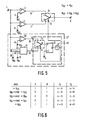
- Fig. 1 shows a first embodiment of a circuit having an input terminal 1 coupled to a first inputs (+) of a first and a second comparator device 2 and 3 respectively.
- the two comparator devices each comprise one comparator.
- a second input (-) of the first comparator device 2 is coupled to a point 4 of constant potential.
- a second input (-) of the second comparator device 3 is coupled to a point 5 of constant potential.
- Outputs 6 and 7 of the comparator device 2 and 3 respectively are coupled to respective inputs c and a of switching means S1 in the form of a controllable switch.
- An output b of the switch S1 is coupled to an output terminal 8 of the circuit.
- the comparator 2 is adapted to supply a first electric signal (a logic "1" signal) exclusively if the input terminal 1 receives pulses shows relative amplitude in relation to the reference level U ref exceeds a first value.
- a potential U D1 is how applied to the point 4 of constant potential.
- the first value is then equal to U D1 -U ref .
- U ref need not necessarily be zero volts, but may alternatively be a specific non-zero direct voltage. It should be noted here that the word "exclusively" given above, means that the comparator 2 supplies the first electric signal only if the pulse exceeds the first value. The comparator 2 does not supply the first electric signal if the pulse has relative amplitude lower than the first value.
- the comparator 3 is adapted to supply a second electric signal (a logic "1" signal) if the input terminal 1 receives pulses whose relative amplitude in relation to U ref exceeds a second value. Since the potential U D2 is applied to point 5, the second value will be equal to U d2 -U ref . In this embodiment the third, the fourth and the first value are equal to each other and the second value is equal to the fifth value.
- the control signal generator means shown in the circuit of Fig. 1 comprises the elements situated within the dashed block 13. It is obvious that the comparators which provide the pulse detection are also used for deriving the control signal which is applied to the control signal input 12 of the switch S1.
- Fig. 3 shows the circuit of Fig. 1 extended to detect pulses of positive and negative polarity relative to the reference level U ref .
- the first comparator device 2 comprises a first and a second comparator 2.1 and 2.2 respectively and an S-R flip-flop 20.
- the second comparator device 3′ now comprises a first and a second comparator 3.1 and 3.2 respectively and an S-R flip-flop 21.
- the input terminal 1 is coupled to the non-inverting inputs (+) of the comparators 2.1 and 3.1 and to the inverting inputs (-) of the comparators 2.2 and 3.2.
- the inverting inputs (-) of the comparators 2.1 and 3.1 are coupled to a point of constant potential, 4.1 and 5.1 respectively.
- the non-inverting inputs (+) of the comparators 2.2 and 3.2 are coupled to a point of constant potential, 4.2 and 5.2 respectively.
- the outputs 6.1 and 6.2 of the comparators 2.1 and 2.2 respectively are coupled to the set input and the reset input respectively of the flip-flop 20.
- the Q-output of the flip-flop 20 is coupled to the input terminal c of the switch S1.
- the outputs 7.1 and 7.2 of the comparators 3.1 and 3.2 respectively are coupled to the set input and the reset input respectively of the flip-flop 21.
- the Q-output of the flip-flop 21 is coupled to the input terminal ⁇ of the switch S1.
- the outputs 6.1 and 7.1 of the comparators 2.1 and 3.1 respectively are coupled to the inputs of the AND gate 9.
- the outputs 6.2 and 7.2 of the comparators 2.2 and 3.2 respectively are coupled to inputs of an AND gate 22.
- the outputs of the two AND gates are coupled to the count input cl of the counter 10 via an OR gate 24.
- the outputs 7.1 and 7.2 of the comparators 3.1 and 3.2 respectively are coupled to the count input cl of the counter 11 via an OR gate 23.
- the pulses applied to the comparators 3.1 and 3.2 via the input terminal 1 are first amplified in an amplifier 25. In the case of an appropriate choice of the gain factor of the amplifier 25 equal potentials may be applied to points 4.1 and 5.1 and to points 4.2 and 5.2.
- the comparator 4.1 supplies a (third) electric signal (logic "1") when the input terminal 1 receives a pulse whose amplitude relative to the reference level U ref exceeds the first value (equal to U D1 -U ref ) in a positive sense relative to U ref .
- the comparator 4.2 supplies a (fourth) electric signal (logic "1") when the input terminal 1 receives a pulse whose amplitude relative to the reference level U ref exceeds the first value in a negative sense relative to U ref
- the comparator 3.1 supplies a (fifth) electric signal (logic "1") when the input terminal 1 receives a pulse whose relative amplitude in relation to U ref exceeds the second value (equal to U D2 -U ref ) in a positive sense relative to U ref
- the comparator 3.2 supplies a (sixth) electric signal (logic "1") when the input terminal 1 receives a pulse whose relative amplitude in relation to U ref exceeds the second value in a negative sense relative to U ref .
- the pulses detected by the comparators are not transferred to the output terminal 8 but instead a squarewave is transferred whose rising and falling edges indicate the detection instants of the detected pulses. It is obvious that in the present embodiment the comparators 2.1, 2.2, 3.1 and 3.2 form part of the control signal generator means 13′.
- the counter 10 counts N1 pulses of an amplitude larger than U D1 . These pulses need not necessarily be N1 consecutive pulses of an amplitude larger than U D1 .
- the control signal generator means 13 and 13′ may be adapted in such a way that the counter 10 can count only N1 consecutive pulses of an amplitude larger than U D1 before it supplies a "high" control signal to the control signal input 12 of the switching means S1.
- Fig. 1a shows the control signal generator means 13 of Fig. 1 which, in addition comprises a detector 15, an OR gate 16, an AND gate 17 and an inverter 18.
- the input terminal 1 is coupled to a first input (+) of the comparator device 30, which is constructed as a single comparator, and to a first input 23 of the second comparator device 31.
- the other (-) input of the comparator 30 is coupled to a point 34 of constant potential.
- a second input 35 and a third input 36 of the comparator 31 are coupled to points of constant potential 37 and 38 respectively.
- the outputs 39 and 40 of the comparators 30 and 31 are respectively coupled to the inputs c and a of the switch S2.
- the output terminal b of the switch S2 is coupled to the D input of the flip-flop 32.
- the Q output of the flip-flop 32 is coupled to the control signal input 12 of the switch S1 and to the control signal input 41 of the switch S2 via a delay 32′.
- the switch S1 is in position c-b and the switch S2 is in position a-b. If the output signal of the flip-flop 32 is logic "0”, the switches S1 and S2 are in positions a-b and c-b respectively.
- the detection device comprising the comparators 2 and 3 and the switch S1, again operates in the same way as the corresponding components in the circuit shown in Fig. 1.
- the operation of the control signal generator means 13 ⁇ is illustrated by means of the Table in Fig. 6.
- the comparator 30 outputs a (third) signal (logic "1") if the pulse applied to the input terminal 1 has a relative amplitude in relation to U ref larger than the third value, or if the amplitude of the pulse is larger than U D3 , i.e. the potential on point 34. This is indicated in column A in Fig. 6. This column specifies the output signal of the comparator 30.
- the comparator 31 delivers a (fourth) electric signal, being logic "1", on its output if a pulse is an amplitude relative to U ref between the third value and the fourth value is applied to the input terminal 1. In other words: if the amplitude of the pulse is situated between U D3 and U D4 . If a pulse having a relative amplitude between the fourth and the fifth value is applied to the input terminal 1 the comparator 31 will supply a (fifth) electric signal, being logic "0". All this is indicated in column B of the Table in Fig. 6. For a correct operation of the comparator 31 potentials equal to U D4 and UDS are applied to the points 37 and 38 respectively.
- U D5 ⁇ U D4 ⁇ U D3 and U D2 ⁇ U D1 .
- U D1 may be selected to be equal to U D1 and U D5 to be equal to U D2 .
- the choice U D5 ⁇ U D2 ⁇ U D1 ⁇ U D4 ⁇ U D3 is made.
- the circuit operates as follows, assuming that the switches S1 and S2 are initially in positions a-b and c-b respectively. This means that the output of the flip-flop 32 is logic "0". It is also assumed that U D5 is equal to U D2 .
- a pulse having an amplitude between U D2 and U D3 is applied to the input terminal 1.
- This pulse is transferred to the output terminal 8 via the comparator 3 and the switch S1 Substantially at the instant at which the pulse is transferred to the input terminal 1 a clock pulse is derived, which is applied to the clock input cl of the flip-flop 32. Since the output 39 of the comparator 30 is logic "0" under the influence of the applied pulse, the Q output of the flip-flop 32 remains “0” after this clock pulse. If now a pulse of an amplitude larger than U D3 is applied this pulse is also transferred to the output terminal 8 the comparator 3 and the switch S1. Moreover, the output of the comparator 30 goes "high".
- the clock pulse cl applied to the flip-flop 32 may be derived, for example, from the output signal of the comparator having the smallest threshold value. If U D5 is equal to U D2 this may therefore be the comparator 3.
- the output of the comparator 3 may be coupled to a monostable via a delay, which monostable has its output coupled to the clock input of the flip-flop 32. It is obvious that the delay should be selected in such a way that the clock pulse cl appears at such an instant that the pulse is still present on the input terminal 1.
- the positions of the switches S1 and S2 in Fig. 6 relate to the pulse which follows the pulse having an amplitude as indicated in the left-hand column "ampl" in the Table given in Fig. 6.
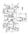
- Fig.7 shows a circuit for detecting pulses of positive and negative amplitudes relative to the reference level, which circuit also exhibits the hysteresis effect.
- the comparator device 2 ⁇ comprises two comparators 2.1 and 2.2 having their outputs 6.1 and 6.2 coupled to respective inputs 51.1 and 51.2 of the switching means S1.
- the comparator device 3 ⁇ again comprises two comparators 3.1 and 3.2, whose outputs 7.1 and 7.2 are coupled to respective inputs 52.1 and 52.2 of the switching means S1′
- the switching means S1′ comprise two switches S11 and S12 and a flip-flop 53.
- the input 53.1 i.e.
- the first sub-input of the first input of the switching means S1′ is coupled to the terminal c of the switch S11
- the input 52.1 being the first sub-input of the second input of the switching means S1′, is coupled to the terminal a of the switch S11
- the input 51.2 i.e. the second sub-input of the first input of the switching means S1′, is coupled to the terminal c of the switch S12
- the input 52.2 i.e. the second sub-input of the second input of the switching means S1′, is coupled to the terminal a of the switch S12
- the terminals b of the switches S11 and S12 are coupled to the set input and the reset input respectively of the flip-flop 53.
- the Q output of the flip-flop 53 constitutes the output of the switching means S1′ which output is coupled to the output terminal 8.
- the control signal generator means 13′′′ now comprise a first comparator device 30′ comprising a first and a second comparator 30.1 and 30.2 respectively, a second comparator device 31′ comprising a first and a second comparator 31.1 and 31.2 respectively, and a signal combination unit 45′.
- the comparator 30.1 is identical to and operates in a manner similar to the comparator 30 in Fig. 5.
- the comparator 31.1 is identical to and operates similarly to the comparator 31 in Fig. 5.
- the comparators 2.1 and 3.1 are identical to and operates similarly to the comparators 2 and 3 respectively in Fig. 5.
- the comparator 2.2 in Fig. 7 operates in the same way as the combination of the comparator 2.2 and the amplifier 25 in Fig. 3.
- the comparator 3.2 in Fig. 7 operates in the same way as the combination of the comparator 3.2 in the amplifier 25 in Fig. 3.
- the comparator 30.2 has an inverting input coupled to the input terminal 1 and a non-inverting input coupled to the point 34.2 of constant potential.
- the potential -U D3 which is referred to the reference level U ref , is applied to said point.
- This comparator delivers an (eleventh) electric signal, logic "1", on its output 39.2 if a pulse applied to the input terminal 1 has an amplitude which exceeds the third value U D3 in a negative sense relative to U ref .
- the comparator 31.2 has an input 33.2 coupled to the input terminal 1, has an input 35.2 coupled to the point 37.2 of constant potential (-U D4 relative to U ref ), and has an input 36.2 coupled to the point 38.2 of constant potential (-U D5 relative to U ref ).
- the comparator 31.2 supplies a (thirteenth) electric signal, logic "1", when the input terminal 1 receives a pulse having an amplitude which, in a negative sense relative to U ref , lies between the third and the fourth value, and supplies a (fifteenth) electric signal, logic "0", when the input terminal 1 receives a pulse having an amplitude which, in a negative sense relative to U ref , lies between the fourth and the fifth value.
- the outputs 39.1, 39.2, 40.1 and 40.2 of the comparators are coupled to inputs of the signal combination unit 45′.
- the signal-combination unit 45′ supplies a control signal for the switching means S1′.
- This control signal comprises two sub-control signals CS1 and CS2, which are applied to the control signal inputs 12.1 and 12.2 respectively via the outputs 46.1 and 46.2 respectively.
- the sub-control signal CS1 controls the switch S11 and the sub-control signal CS2 controls the switch S12.
- the circuit operates as follows.
- the switch S12 is in position a-b, see Fig. 8c.
- the position of the switch S11 is irrelevant and may be position "a-b" or position "c-b", see Fig. 8b.
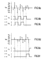
- a positive pulse having an amplitude larger than U D3 is applied to the input terminal 1, see Fig. 8a.
- the control signal generator means 13′′′ will generate a control signal CS2, causing the switch S12 to be set to position c-b, see Fig. 8c.
- the switch S11 will be set to position a-b if it is not yet in this position, see Fig. 8b.
- the switch S11 is reset to position a-b, see Fig. 8b.
- a negative pulse of an amplitude larger than U D4 but smaller than U D3 is applied to the input terminal 1, see Fig. 8a.
- the switch S11 is set to position c-b, see Fig. 8b and the switch S12 is set to position a-b.
- the positive pulse having an amplitude larger than U D5 but smaller than U D4 received at that the instant t5 only causes the switch S11 to be set to position a-b, see Fig. 8b.
- Consecutive pulses of an amplitude between U D5 and U D4 such as the pulse at the instant t6, see Fig. 8a, no longer cause the settings of the switches S11 and S12 to change.
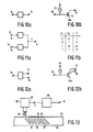
- Fig. 9 shows an embodiment of the signal combination unit 45′ in Fig. 7.
- the circuit comprises I2L logic devices as illustrated in Fig. 10a.
- Fig. 10b shows the circuit diagram of the device in Fig. 10a.
- the input 70 of the device is coupled to the base of an npn transistor 72.
- the collector of this transistor is coupled to the output 71 of the device.
- the positive supply voltage (+) is coupled to the base of the transistor 72 via a current source 73, which transistor has its emitter coupled to earth.
- the device operates as an inverter. When a logic "0" signal is applied to the input 70 the output 71 will be logic "1" and vice versa .
- Fig. 12a shows a devive having two outputs 77 and 78.
- the circuit diagram of this device is shown in Fig. 12b. If the signal on the input 76 is logic "1" all the outputs are logic "0". If the input signal is logic "0" the output state will depend on whether an output is coupled to an output of another device. If the output of this other device is "high” the output of the device in Fig. 12 will also be “high”. In the other case the output will be "low”. The operation of devices having more than two outputs is identical to the operation of the device shown in Fig. 12.
- Fig. 9 shows not only an example of the signal combination unit 45′ but gives also more details of the two switches S11 and S12 and of the output flip-flop 53. Specifically, the gates G1, G2, G3 and G4 constitute the switch S11 and the gates G16, G17, G18 and G19 constitute the switch S12. Further, the gates G27, G28, F29, G3O constitute the output flip-flop 53.
- the signal C1 which is the output signal of the comparator 2.1, is applied to the circuit shown in Fig.9 via the terminal 91. This means that C1 is logic "1" if a pulse has an amplitude larger than U D1 .
- the signal D1 i.e. the output signal of the comparator 2.2, is applied to the terminal 93. This means that D1 is logic “1” if the amplitude of a negative pulse is larger in absolute value than U D1 .
- the signal D2, which is the output signal of the comparator 3.2, is applied to the terminal 94, D2 consequently being logic “1” if the amplitude of a negative pulse is larger in absolute value than U D2 .
- the signal A1, which is the output signal of the comparator 30.1, is applied to the terminal 95. This means that A1 is logic "1” if the amplitude of a pulse is larger than U D3 .
- the signal A2, which is the output signal of the comparator 30.2, is applied to the terminal 96.
- A2 is logic "1” if the amplitude of a negative pulse is larger in absolute value than U D3 .
- the signal B1′ is applied to the terminal 97.
- B1′ logic “0” if the amplitude of a pulse is larger than U D4 .
- the signal B2′ is applied to the terminal 98.
- B2′ is logic "0” if the amplitude of a negative pulse is larger in absolute value than U D4 .
- the circuit operates as follows.
- setting of the flip-flop 53 is determined by a negative pulse having an amplitude of an absolute value larger than U D1 and not by a negative pulse having an amplitude of an absolute value larger than U D2 (but smaller than U D1 !).
- the gate G12 can go "high” if a negative pulse whose absolute amplitude is larger than U D3 should appear on the input terminal 1. This is because of the signal B2′ applied to the terminal 98.
- the gate G11 now goes “low”, so that the signal A2 can no longer have any effect.
- the gate G1 goes “high”, causing S11 to be set. In Fig. 7 this means that the switch S11 is in position c-b.
- "setting" of S11 is achieved by a negative pulse having an amplitude whose absolute value is larger than U D4 and not by a negative pulse having an amplitude whose absolute value is larger than U D3 .
- FF2 is reset by means of the signal C2 upon a positive pulse of an amplitude larger than U D2 .
- S11 is reset the signal C2 is inhibited in the gate G6.
- S12 is set the signal D2 is inhibited in the gate G15. This means that a positive pulse of large amplitude is anticipated on account of the fact that the negative pulse preceding it had a large amplitude, and vice versa .
- a positive pulse larger than U D1 resets the flip-flop 54 by means of the signal C1 in the same way as the negative pulse having an amplitude larger in absolute value than U D1 has set the flip-flop 53 by means of the signal C1. Conversely, if a positive pulse of an amplitude smaller than U D1 is received the flip-flop 53 is not reset. Since B1′ now remains "high" S12 is not set via the signal path G9, G10. This means that at the negative side the detection level is situated at U D2 . In turn, this means that G15 is no longer inhibited so that a negative pulse having an amplitude larger in absolute value than U D2 , i.e. the signal D2, can set the flip-flop 53.
- the flip-flop 53 has already been set because the preceding positive pulse has not caused a reset signal for the flip-flop. This negative pulse does not intersect the -U D3 level. As a result of this, the input A2 remains "low” and the switch S11 is not set. Upon the next negative pulse the flip-flop 53 is reset by means of the signal C2.
- the flip-flop 53 is each time set and reset by the signals D2 and C2 respectively.
- Fig. 13 illustrates the use of the circuit in accordance with the invention in a video recorder during reading of a video signal which has been recorded in tracks 81 which are inclined relative to the longitudinal direction of the record carrier 80.
- the record carrier 80 also has an auxiliary track 82 at the edge of and in the longitudinal direction of the record carrier.
- track control pulses 83 are recorded, which are used for correctly controlling the speed of transport of the record carrier 80.
- the pulses 83 are read by means of a stationary read head 84.
- the pulses read by the head 84 are applied to a read amplifier 86.
- the read amplifier 86 may be, for example, the write/read device described in the Applicants Netherlands Patent Application no. (PHN 13.054).
- the output 87 of the read amplifier 86 is coupled to the input terminal 1 of the circuit 85. Consequently, this circuit may be constructed in the same way as one of the embodiments described with reference to Figs. 1 to 8.
Landscapes
- Engineering & Computer Science (AREA)
- Signal Processing (AREA)
- Manipulation Of Pulses (AREA)
- Details Of Television Scanning (AREA)
- Radar Systems Or Details Thereof (AREA)
- Stabilization Of Oscillater, Synchronisation, Frequency Synthesizers (AREA)
- Picture Signal Circuits (AREA)
Applications Claiming Priority (2)
| Application Number | Priority Date | Filing Date | Title |
|---|---|---|---|
| NL8902225A NL8902225A (nl) | 1989-09-05 | 1989-09-05 | Schakeling voor het detekteren van impulsen, en videorecorder voorzien van de schakeling. |
| NL8902225 | 1989-09-05 |
Publications (2)
| Publication Number | Publication Date |
|---|---|
| EP0416695A1 true EP0416695A1 (de) | 1991-03-13 |
| EP0416695B1 EP0416695B1 (de) | 1996-12-04 |
Family
ID=19855263
Family Applications (1)
| Application Number | Title | Priority Date | Filing Date |
|---|---|---|---|
| EP90202326A Expired - Lifetime EP0416695B1 (de) | 1989-09-05 | 1990-09-03 | Impulsdetektionsschaltung und Videorekorder mit dieser Schaltung |
Country Status (8)
| Country | Link |
|---|---|
| US (1) | US5539340A (de) |
| EP (1) | EP0416695B1 (de) |
| JP (1) | JP2992584B2 (de) |
| KR (1) | KR100190790B1 (de) |
| AT (1) | ATE146007T1 (de) |
| DE (1) | DE69029299T2 (de) |
| ES (1) | ES2097131T3 (de) |
| NL (1) | NL8902225A (de) |
Cited By (1)
| Publication number | Priority date | Publication date | Assignee | Title |
|---|---|---|---|---|
| GB2258079A (en) * | 1991-07-19 | 1993-01-27 | Samsung Electronics Co Ltd | A video index search system (viss) with residual signal compensation |
Families Citing this family (9)
| Publication number | Priority date | Publication date | Assignee | Title |
|---|---|---|---|---|
| EP0774726A1 (de) * | 1995-11-03 | 1997-05-21 | STMicroelectronics S.r.l. | Vorrichtung zum Selektieren von analogen Spannungssignalen |
| US5889419A (en) * | 1996-11-01 | 1999-03-30 | Lucent Technologies Inc. | Differential comparison circuit having improved common mode range |
| DE19702303A1 (de) * | 1997-01-23 | 1998-07-30 | Philips Patentverwaltung | Schaltungsanordnung zum Erzeugen eines Ausgangssignals |
| JPH11345447A (ja) * | 1998-03-30 | 1999-12-14 | Mitsubishi Electric Corp | Viss信号検出回路 |
| US6038266A (en) * | 1998-09-30 | 2000-03-14 | Lucent Technologies, Inc. | Mixed mode adaptive analog receive architecture for data communications |
| DE19905053C2 (de) * | 1999-02-08 | 2003-05-08 | Infineon Technologies Ag | Komparatorschaltung |
| US7130340B1 (en) * | 2000-10-27 | 2006-10-31 | Sun Microsystems, Inc. | Noise margin self-diagnostic receiver logic |
| JP4254683B2 (ja) * | 2004-10-04 | 2009-04-15 | 株式会社デンソー | コンパレータ切替え回路 |
| US8519744B2 (en) * | 2011-06-28 | 2013-08-27 | General Electric Company | Method of utilizing dual comparators to facilitate a precision signal rectification and timing system without signal feedback |
Citations (6)
| Publication number | Priority date | Publication date | Assignee | Title |
|---|---|---|---|---|
| US3593334A (en) * | 1968-11-29 | 1971-07-13 | Burroughs Corp | Pulse discrimination system |
| US4167028A (en) * | 1978-04-13 | 1979-09-04 | Recortec, Inc. | Method and an apparatus for time signal encoding/decoding |
| DE3030531A1 (de) * | 1980-08-13 | 1982-03-04 | Institut für Rundfunktechnik GmbH, 8000 München | Verfahren und schaltungsanordnung zum demodulieren eines von einem magnetischen informationstraeger abgenommenen, ternaer modulierten datensignals |
| EP0047955A2 (de) * | 1980-09-16 | 1982-03-24 | Kabushiki Kaisha Toshiba | Wellenformerschaltung |
| GB2120030A (en) * | 1982-03-04 | 1983-11-23 | Sansui Electric Co | Digital signal demodulator circuit |
| EP0248945A2 (de) * | 1986-06-09 | 1987-12-16 | General Service Electronics GmbH | Verfahren zum Übertragen eines Informationskodes auf der Synchronspur eines Videobandes, Vorrichtung zur Durchführung des Verfahrens sowie nach dem Verfahren hergestelltes Videoband |
Family Cites Families (2)
| Publication number | Priority date | Publication date | Assignee | Title |
|---|---|---|---|---|
| KR910003457B1 (ko) * | 1987-09-17 | 1991-05-31 | 삼성전자 주식회사 | 광 디스크 드라이버의 데이타 트랙 카운터회로 |
| JPH01265718A (ja) * | 1988-04-18 | 1989-10-23 | Toshiba Corp | シュミットトリガ回路 |
-
1989
- 1989-09-05 NL NL8902225A patent/NL8902225A/nl not_active Application Discontinuation
-
1990
- 1990-09-03 EP EP90202326A patent/EP0416695B1/de not_active Expired - Lifetime
- 1990-09-03 DE DE69029299T patent/DE69029299T2/de not_active Expired - Fee Related
- 1990-09-03 ES ES90202326T patent/ES2097131T3/es not_active Expired - Lifetime
- 1990-09-03 AT AT90202326T patent/ATE146007T1/de not_active IP Right Cessation
- 1990-09-05 JP JP2233430A patent/JP2992584B2/ja not_active Expired - Lifetime
- 1990-09-05 KR KR1019900013965A patent/KR100190790B1/ko not_active Expired - Fee Related
-
1994
- 1994-10-31 US US08/332,615 patent/US5539340A/en not_active Expired - Fee Related
Patent Citations (6)
| Publication number | Priority date | Publication date | Assignee | Title |
|---|---|---|---|---|
| US3593334A (en) * | 1968-11-29 | 1971-07-13 | Burroughs Corp | Pulse discrimination system |
| US4167028A (en) * | 1978-04-13 | 1979-09-04 | Recortec, Inc. | Method and an apparatus for time signal encoding/decoding |
| DE3030531A1 (de) * | 1980-08-13 | 1982-03-04 | Institut für Rundfunktechnik GmbH, 8000 München | Verfahren und schaltungsanordnung zum demodulieren eines von einem magnetischen informationstraeger abgenommenen, ternaer modulierten datensignals |
| EP0047955A2 (de) * | 1980-09-16 | 1982-03-24 | Kabushiki Kaisha Toshiba | Wellenformerschaltung |
| GB2120030A (en) * | 1982-03-04 | 1983-11-23 | Sansui Electric Co | Digital signal demodulator circuit |
| EP0248945A2 (de) * | 1986-06-09 | 1987-12-16 | General Service Electronics GmbH | Verfahren zum Übertragen eines Informationskodes auf der Synchronspur eines Videobandes, Vorrichtung zur Durchführung des Verfahrens sowie nach dem Verfahren hergestelltes Videoband |
Non-Patent Citations (1)
| Title |
|---|
| RUNDFUNKTECHNISCHE MITTEILUNGEN. vol. 20, no. 5, October 1976, NORDERSTEDT DE pages 188 - 194; ALTMANN et al.: "AUFZEICHNUNG UND ABTASTUNG DES ZEITCODES" * |
Cited By (2)
| Publication number | Priority date | Publication date | Assignee | Title |
|---|---|---|---|---|
| GB2258079A (en) * | 1991-07-19 | 1993-01-27 | Samsung Electronics Co Ltd | A video index search system (viss) with residual signal compensation |
| GB2258079B (en) * | 1991-07-19 | 1995-04-19 | Samsung Electronics Co Ltd | Control signal reproducing circuit |
Also Published As
| Publication number | Publication date |
|---|---|
| KR100190790B1 (ko) | 1999-06-01 |
| US5539340A (en) | 1996-07-23 |
| DE69029299D1 (de) | 1997-01-16 |
| ATE146007T1 (de) | 1996-12-15 |
| KR910006953A (ko) | 1991-04-30 |
| NL8902225A (nl) | 1991-04-02 |
| ES2097131T3 (es) | 1997-04-01 |
| JPH0393063A (ja) | 1991-04-18 |
| EP0416695B1 (de) | 1996-12-04 |
| JP2992584B2 (ja) | 1999-12-20 |
| DE69029299T2 (de) | 1997-05-28 |
Similar Documents
| Publication | Publication Date | Title |
|---|---|---|
| JPS62236381A (ja) | ブラシレス直流モ−タの制御回路 | |
| EP0416695A1 (de) | Impulsdetektionsschaltung und Videorekorder mit dieser Schaltung | |
| US4338640A (en) | Speed control system for a multiple speed tape recording and reproducing apparatus | |
| US4637003A (en) | Amplitude modulated high frequency signal detection device | |
| US4535371A (en) | Recording channel with signal controlled integrated analog circuits | |
| US4626936A (en) | Relative velocity control device for magnetic recording and reproducing apparatus | |
| EP0359019B1 (de) | Spurregelkreis für ein magnetisches Bandgerät mit Schraubenlinienabtastung | |
| US4001884A (en) | Apparatus and method for recording and reproducing digital-data | |
| US4074149A (en) | Peak detecting with constant fractional offset | |
| EP0043739A1 (de) | Nachführsystem | |
| US4222081A (en) | Information reading device for a multitrack storage device | |
| US3248570A (en) | Signal discriminator circuit | |
| JP3417585B2 (ja) | 情報信号記録装置 | |
| US5315449A (en) | Time code signal processing circuit for removing and restoring variation in slew rate | |
| US3402402A (en) | Apparatus for translating magnetically recorded binary data | |
| JPH0553026B2 (de) | ||
| JPS6390050A (ja) | 磁気記録再生装置 | |
| JP2933449B2 (ja) | 自動利得制御回路及びこれを用いたデータ記憶装置 | |
| JP2957843B2 (ja) | 信号のデューティ比識別回路 | |
| KR940006925Y1 (ko) | 하드디스크 드라이브의 펄스검출 제어회로 | |
| KR980011231A (ko) | 디지털 브이씨알의 캡스턴 서보회로 | |
| JPH0630198B2 (ja) | 磁気記録再生装置 | |
| JPH0644513A (ja) | 包絡線検波器 | |
| JPH0463453B2 (de) | ||
| JPS6346891B2 (de) |
Legal Events
| Date | Code | Title | Description |
|---|---|---|---|
| PUAI | Public reference made under article 153(3) epc to a published international application that has entered the european phase |
Free format text: ORIGINAL CODE: 0009012 |
|
| AK | Designated contracting states |
Kind code of ref document: A1 Designated state(s): AT DE ES FR GB |
|
| 17P | Request for examination filed |
Effective date: 19910909 |
|
| 17Q | First examination report despatched |
Effective date: 19940808 |
|
| GRAH | Despatch of communication of intention to grant a patent |
Free format text: ORIGINAL CODE: EPIDOS IGRA |
|
| GRAH | Despatch of communication of intention to grant a patent |
Free format text: ORIGINAL CODE: EPIDOS IGRA |
|
| GRAA | (expected) grant |
Free format text: ORIGINAL CODE: 0009210 |
|
| AK | Designated contracting states |
Kind code of ref document: B1 Designated state(s): AT DE ES FR GB |
|
| PG25 | Lapsed in a contracting state [announced via postgrant information from national office to epo] |
Ref country code: AT Effective date: 19961204 |
|
| REF | Corresponds to: |
Ref document number: 146007 Country of ref document: AT Date of ref document: 19961215 Kind code of ref document: T |
|
| REF | Corresponds to: |
Ref document number: 69029299 Country of ref document: DE Date of ref document: 19970116 |
|
| ET | Fr: translation filed | ||
| REG | Reference to a national code |
Ref country code: ES Ref legal event code: FG2A Ref document number: 2097131 Country of ref document: ES Kind code of ref document: T3 |
|
| PLBE | No opposition filed within time limit |
Free format text: ORIGINAL CODE: 0009261 |
|
| STAA | Information on the status of an ep patent application or granted ep patent |
Free format text: STATUS: NO OPPOSITION FILED WITHIN TIME LIMIT |
|
| 26N | No opposition filed | ||
| REG | Reference to a national code |
Ref country code: FR Ref legal event code: CD |
|
| REG | Reference to a national code |
Ref country code: ES Ref legal event code: PC2A |
|
| PGFP | Annual fee paid to national office [announced via postgrant information from national office to epo] |
Ref country code: ES Payment date: 20010918 Year of fee payment: 12 |
|
| PGFP | Annual fee paid to national office [announced via postgrant information from national office to epo] |
Ref country code: FR Payment date: 20010925 Year of fee payment: 12 |
|
| PGFP | Annual fee paid to national office [announced via postgrant information from national office to epo] |
Ref country code: GB Payment date: 20011001 Year of fee payment: 12 |
|
| PGFP | Annual fee paid to national office [announced via postgrant information from national office to epo] |
Ref country code: DE Payment date: 20011121 Year of fee payment: 12 |
|
| REG | Reference to a national code |
Ref country code: GB Ref legal event code: IF02 |
|
| PG25 | Lapsed in a contracting state [announced via postgrant information from national office to epo] |
Ref country code: GB Free format text: LAPSE BECAUSE OF NON-PAYMENT OF DUE FEES Effective date: 20020903 |
|
| PG25 | Lapsed in a contracting state [announced via postgrant information from national office to epo] |
Ref country code: ES Free format text: LAPSE BECAUSE OF NON-PAYMENT OF DUE FEES Effective date: 20020904 |
|
| PG25 | Lapsed in a contracting state [announced via postgrant information from national office to epo] |
Ref country code: DE Free format text: LAPSE BECAUSE OF NON-PAYMENT OF DUE FEES Effective date: 20030401 |
|
| GBPC | Gb: european patent ceased through non-payment of renewal fee |
Effective date: 20020903 |
|
| PG25 | Lapsed in a contracting state [announced via postgrant information from national office to epo] |
Ref country code: FR Free format text: LAPSE BECAUSE OF NON-PAYMENT OF DUE FEES Effective date: 20030603 |
|
| REG | Reference to a national code |
Ref country code: FR Ref legal event code: ST |
|
| REG | Reference to a national code |
Ref country code: ES Ref legal event code: FD2A Effective date: 20031011 |