EP0418149A2 - Durch Mikrokomputer gesteuerter Funkempfänger mit Synthesizer - Google Patents
Durch Mikrokomputer gesteuerter Funkempfänger mit Synthesizer Download PDFInfo
- Publication number
- EP0418149A2 EP0418149A2 EP90402503A EP90402503A EP0418149A2 EP 0418149 A2 EP0418149 A2 EP 0418149A2 EP 90402503 A EP90402503 A EP 90402503A EP 90402503 A EP90402503 A EP 90402503A EP 0418149 A2 EP0418149 A2 EP 0418149A2
- Authority
- EP
- European Patent Office
- Prior art keywords
- frequency
- clock
- clock signal
- signal
- electronic apparatus
- Prior art date
- Legal status (The legal status is an assumption and is not a legal conclusion. Google has not performed a legal analysis and makes no representation as to the accuracy of the status listed.)
- Granted
Links
Images

Classifications
-
- H—ELECTRICITY
- H04—ELECTRIC COMMUNICATION TECHNIQUE
- H04B—TRANSMISSION
- H04B1/00—Details of transmission systems, not covered by a single one of groups H04B3/00 - H04B13/00; Details of transmission systems not characterised by the medium used for transmission
- H04B1/06—Receivers
- H04B1/10—Means associated with receiver for limiting or suppressing noise or interference
-
- H—ELECTRICITY
- H04—ELECTRIC COMMUNICATION TECHNIQUE
- H04B—TRANSMISSION
- H04B15/00—Suppression or limitation of noise or interference
- H04B15/02—Reducing interference from electric apparatus by means located at or near the interfering apparatus
- H04B15/04—Reducing interference from electric apparatus by means located at or near the interfering apparatus the interference being caused by substantially sinusoidal oscillations, e.g. in a receiver or in a tape-recorder
-
- H—ELECTRICITY
- H04—ELECTRIC COMMUNICATION TECHNIQUE
- H04B—TRANSMISSION
- H04B2215/00—Reducing interference at the transmission system level
- H04B2215/064—Reduction of clock or synthesizer reference frequency harmonics
Definitions
- the present invention relates generally to radio receivers and, more particularly, is directed to electronic apparatus having a synthesizer-type receiver which is preferably combined with a cassette type tape player and/or a compact disk (CD) player in a unitary assembly.
- a synthesizer-type receiver which is preferably combined with a cassette type tape player and/or a compact disk (CD) player in a unitary assembly.
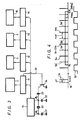
- a known electronic apparatus comprises, in a unitary assembly, an AM/FM receiving section 1 of the synthesizer-type, a CD player section 2, a cassette tape player or deck section 3, a main or master micro-computer 10, slave micro-computers 11, 12 and 13 for controlling the AM/FM receiver section 1, the CD player section 2 and the cassette tape player section 3, respectively, and an additional slave micro-computer 14 for processing control signals supplied from or to a remote control receiver 15 and transmitted from or to a remote commander (not shown).
- the AM/FM receiver section 1 of the synthesizer-type conventionally includes a phase locked loop (PLL) in which a frequency-dividing ratio signal from the micro-computer 11 determines the dividing ratio of a variable frequency-dividing circuit (not shown) in the PLL and thereby determines the receiving frequency of the receiver section 1.
- PLL phase locked loop
- the micro-computers 11-14 may each be constituted by a 4-bit single chip-type micro-computer, and are all controlled or commanded by the main computer 10.
- the software programs in the micro-computers 11-14 can be easily developed so as to enable the sections 1, 2 and 3 to perform numerous operations and functions.
- the main micro-computer 10 is a micro-processor obtainable from the NEC Corporation under the designation D 753284GC
- the micro-computer 11 is a micro-processor also obtainable from the NEC Corporation under the designation D 1725G
- the micro-computer 12 is obtainable from Sony Corporation under the designation CXP 5078
- the micro-computer 13 is also obtainable from Sony Corporation under the designation CXP 5024
- the microcomputer 14 is obtainable from Mitsubishi Electric Corporation under the designation M 50920.
- a clock signal is required for operation of each of the micro-computers 10-14. If the clock signal CK for the main micro-computer 10 has a relatively high clock frequency fc, for example, of 4.2 MHz, then as shown in Fig. 2A, higher harmonic components Sh of the clock signal CK are distributed within the FM broadcasting frequency band of 76 to 108 MHz. As a result, when the receiver section 1 is operative to receive a FM signal broadcast at a frequency that is equal to one of the higher harmonics Sh of the clock frequency fc, the reception of such broadcast signal is disturbed.
- fc for example, of 4.2 MHz
- the frequency fc of the clock signal CK be decreased to approximately the lowest frequency at which the main computer 10 can be operated, for example, to a frequency of 400 kHz, so that the order of the higher harmonic components Sh of the clock signal CK distributed within the FM broadcasting band is substantially higher than the order of the higher harmonic components within the FM broadcasting band in Fig. 2A.
- the frequency fc of the clock signal CK of the main micro-computer 10 is decreased to about 400 kHz, the level of the higher harmonic components Sh of such clock signal within the FM broadcasting band is so small as to be negligible. More specifically, in the case illustrated in Fig.
- the higher harmonic components Sh of the clock signal CK distributed in the FM broadcasting band when the clock frequency fc is 4.2 MHz are in the range from the 19th order to the 24th order, and at least some of the levels thereof are of sufficient magnitude to produce the undesired disturbance of the FM reception.
- the higher harmonic components Sh of the clock signal CK distributed within the FM broadcasting band are from the 190th order to the 270th order.
- the higher harmonic components Sh of the clock signal CK within the FM broadcasting band range from the 190th order to the 270th order, the levels of such higher harmonic components are, as shown, so small as to be satisfactorily neglected and to ensure that reception of the FM broadcast signal will be undisturbed.
- the frequency of the clock signal CK for the main computer 10 is reduced as described above, for avoiding disturbance of the reception of the FM broadcast signal by the higher harmonic components of such clock signal, the frequencies of the clock signals employed in the micro-computers 11-14 will be similarly decreased for the same reason.
- the processing speeds of the micro-computers 10-14 are correspondingly lowered. Since the micro-computers 11-14 are employed for independently controlling the respective sections 1, 2 and 3 and remote control receiver 15, such computers do not need to operate at high speed. Therefore, the clock frequencies of the micro-computers 11-14 can be reduced, as described above, to ensure that the higher harmonic components of the clock signals employed in the micro-computers 11-14 have negligible levels.
- the main micro-computer 10 exerts overall system control of the electronic apparatus and the micro-computers 11-14 are, in turn, operated under the control of the main micro-computer 10 so that, if the frequency fc of the clock signal CK of the main micro-computer 10 is lowered, for example, to 400 kHz, as described above, the correspondingly lowered processing speed of the main micro-computer 10 reduces the range of operations of the receiver section 1, the CD player section 2, the tape cassette player section 3 and the remote control receiver 15 can be controlled by the main computer.
- the reduced processing speed of the main micro-computer 10 will introduce a time delay in the audio level display. Thus, the audio level indication will not correspond to real time conditions.
- an object of the present invention to provide an electronic apparatus including a synthesizer-type receiver which can prevent disturbance of the reception of an FM broadcast signal by higher harmonic components of a clock signal employed in a micro-computer for controlling the receiver.
- an electronic apparatus comprises a synthesizer-type receiver for selecting a receiving frequency and receiving a signal broadcast at the selected receiving frequency and means for deriving an information signal which corresponds to the selected receiving frequency; control means operable on the basis of a clock signal for controlling operations of at least the synthesizer-type receiver; and clock generating means for providing the clock signal including means responsive to the information signal for shifting the frequency of the clock signal on the basis of such information signal when the selected receiving frequency of the synthesizer-type receiver is a frequency disturbed by a higher harmonic component of the clock signal or of a frequency divided version of the clock signal.
- FIG. 3 it will be seen that many parts of the electronic apparatus embodying the present invention, as there illustrated, are identified by the same reference numerals as were used to identify the corresponding parts in the apparatus of Fig. 1 and will not be again described in detail.
- the main or master micro-computer 10 has a clock oscillator circuit by which the clock signal for the master computer 10 is generated, for example, with a frequency fc of 4.2 MHz.
- Such clock oscillator circuit for the master micro-computer 10 is shown to have a ceramic oscillator 20 for oscillating a clock signal which is connected between clock terminals ⁇ 1 and ⁇ 2 of the main micro-computer 10, and capacitors 21 and 22 respectively connected between clock terminal ⁇ 1 and ground and between clock terminal ⁇ 2 and ground.
- a capacitor 23 and a collector-emitter path of an npn transistor 24 are connected in series between the clock terminal ⁇ 2 and ground.
- the oscillation frequency fc of the ceramic oscillator is selected to achieve a suitably high processing speed of the main micro-computer 10, for example, the oscillation frequency of the ceramic oscillator 20 is selected to be 4.2 MHz.
- the transistor 24 is turned ON, the capacitor 23 is connected in parallel with the capacitor 22 whereby the clock frequency fc of the main micro-computer 10 is shifted by an amount ⁇ f in the lower direction.
- the amount ⁇ f that the clock frequency fc is shifted when the transistor 24 is turned ON is determined as follows:
- n the order of the higher harmonic component Sh of the clock frequency fc which is situated in the FM broadcasting band
- the higher harmonic components Sh′ of the shifted clock frequency fs are located midway between the higher harmonic components Sh of the original clock frequency fc (shown in solid lines in Fig. 4A).
- the micro-computer 11 associated with the synthesizer-type AM/FM receiver 1 is operative to provide an information signal Sf (Fig. 4B) which is related to the receiving frequency fr selected by the synthesizer-type receiver 1 as will now be described.
- the signal sf from the micro-computer 11 is at the high level "1" so long as the selected receiving frequency fr satisfies the below inequality: n (fc - ⁇ f/2) ⁇ fr ⁇ n (fc + ⁇ f/2) (4) At all other times, that is, whenever the selected receiving frequency fr does not satisfy the inequality (4), the signal Sf is at the low level "0".
- the micro-computer 11 Since the micro-computer 11 provides to the synthesizer-type receiver 1 the frequency-dividing ratio for determining the selected receiving frequency fr of the receiver, the micro-computer 11 can readily determine whether or not the frequency-dividing ratio corresponds to the inequality (4) and provide the signal Sf accordingly.
- the signal Sf from the micro-computer 11 is applied to the base of the transistor 24 so that the latter is turned ON when the signal Sf is "1" for shifting the clock frequency fc by the amount ⁇ f, whereas, at all other times, that is, so long as the signal Sf is "0", the clock frequency remains at its normal value fc.
- the higher harmonic components Sh′ thereof are shifted from the frequency n . fc (MHz) of the higher harmonic components Sh (shown by solid lines) of the original clock signal CK by the frequency n . ⁇ f kHz with the result that the shifted higher harmonic components Sh′ do not disturb the FM broadcast signal being received at that time.
- the clock frequency fc of the master micro-computer 10 is shifted when required in response to the selected receiving frequency fr so that the reception of the FM broadcast signal will not, in any case, be disturbed by the higher harmonic components of the clock signal CK. Furthermore, since the clock frequency fc of the master micro-computer 10 is either the original frequency of 4.2 MHz or is equal to that frequency reduced by 95 kHz, it will be appreciated that the master micro-computer 10 is operating, at all times, with a clock of substantially high frequency, and thus can perform the necessary processing at a sufficiently high speed. Therefore, the illustrated electronic apparatus comprising an AM/FM receiver 1, a CD player 2 and a tape cassette player 3 can be operated in a wide variety of operating modes under the control of the master micro-computer 10.
- the higher harmonic components Sh′ of the shifted clock frequency fs are each situated substantially midway between adjacent higher harmonic components Sh (shown by the solid lines on Fig. 4A) of the original clock frequency fc.
- the present invention involves only the addition of the capacitor 23 and the npn transistor 24 to the clock oscillator circuit and a suitable modification of a portion of the program of the micro-computer 11 for operating in the described manner so as to ensure that higher harmonics of the clock frequency will not disturb the received FM broadcast signal. Therefore, a synthesizer-type receiver having the described advantages of the present invention can be provided at little extra cost.
- the previously described embodiment of the invention is intended to avoid disturbance of the received FM broadcast signal by the higher harmonic components Sh of the clock signal CK itself having the clock frequency fc
- the invention can be similarly applied to avoiding disturbance of an FM broadcast signal by higher harmonic components of a frequency divided pulse signal having a frequency of 2.1 MHz, and which results from frequency-dividing by two the clock signal CK within the main micro-computer 10.
- the clock frequency fc is shifted in response to the receiving frequency fr being near to a higher harmonic component of the frequency-divided pulse signal, with the result that such higher harmonic component of the frequency-divided pulse signal is shifted away from the receiving frequency fr.
- the present invention has been described as applied to an electronic apparatus in which a synthesizer-type AM/FM radio receiver is combined with a cassette tape player and a CD player in a unitary assembly, it will be appreciated that the invention is not limited thereto and can be similarly applied to the combination of a synthesizer-type AM/FM radio receiver with either a cassette tape player or a CD player, or merely to the synthesizer-type AM/FM radio receiver in which only one microcomputer is utilized. Furthermore, the present invention can be similarly employed in a synthesizer-type TV tuner for shifting the clock frequency fc and thereby ensuring that higher harmonic components of the clock signal will not disturb a received broadcast television signal.
Landscapes
- Engineering & Computer Science (AREA)
- Computer Networks & Wireless Communication (AREA)
- Signal Processing (AREA)
- Noise Elimination (AREA)
- Circuits Of Receivers In General (AREA)
- Superheterodyne Receivers (AREA)
Applications Claiming Priority (2)
| Application Number | Priority Date | Filing Date | Title |
|---|---|---|---|
| JP01237624A JP3122102B2 (ja) | 1989-09-13 | 1989-09-13 | 受信機 |
| JP237624/89 | 1989-09-13 |
Publications (3)
| Publication Number | Publication Date |
|---|---|
| EP0418149A2 true EP0418149A2 (de) | 1991-03-20 |
| EP0418149A3 EP0418149A3 (en) | 1992-05-27 |
| EP0418149B1 EP0418149B1 (de) | 1996-01-17 |
Family
ID=17018078
Family Applications (1)
| Application Number | Title | Priority Date | Filing Date |
|---|---|---|---|
| EP90402503A Expired - Lifetime EP0418149B1 (de) | 1989-09-13 | 1990-09-11 | Durch Mikrokomputer gesteuerter Funkempfänger mit Synthesizer |
Country Status (5)
| Country | Link |
|---|---|
| US (1) | US5212833A (de) |
| EP (1) | EP0418149B1 (de) |
| JP (1) | JP3122102B2 (de) |
| KR (1) | KR910007287A (de) |
| DE (1) | DE69024888T2 (de) |
Cited By (7)
| Publication number | Priority date | Publication date | Assignee | Title |
|---|---|---|---|---|
| EP0601841A3 (de) * | 1992-12-08 | 1994-08-03 | Sony Corp | |
| GB2292867A (en) * | 1994-09-30 | 1996-03-06 | Matsushita Electric Industrial Co Ltd | Radio system with means to reduce interference due to radiation of clock signal |
| GB2310966A (en) * | 1996-03-04 | 1997-09-10 | Motorola Inc | Method and apparatus for eliminating interference caused by spurious signals in a communication device |
| WO1998009393A1 (de) * | 1996-08-27 | 1998-03-05 | Siemens Aktiengesellschaft | Verfahren zur reduzierung der eigenstörung in mobilfunkgeräten |
| US5875449A (en) * | 1995-08-10 | 1999-02-23 | Nec Corporation | Computer connection available data wireless apparatus with clock signal frequency variable function |
| EP1404040A1 (de) | 2002-09-24 | 2004-03-31 | Alps Electric Co., Ltd. | Interferenzunterdrückung in elektronischen Fahrzeuggeräten |
| WO2007018888A3 (en) * | 2005-07-29 | 2008-02-14 | Silicon Lab Inc | Television receiver suitable for multi-standard operation and method therefor |
Families Citing this family (12)
| Publication number | Priority date | Publication date | Assignee | Title |
|---|---|---|---|---|
| JPH0511565U (ja) * | 1991-07-29 | 1993-02-12 | 日本ビクター株式会社 | ビートカツト装置 |
| JPH0531371U (ja) * | 1991-09-26 | 1993-04-23 | 日本ビクター株式会社 | ビートキヤンセル回路 |
| JP2756739B2 (ja) * | 1991-09-30 | 1998-05-25 | 八重洲無線 株式会社 | 無線通信機 |
| US5646602A (en) * | 1991-10-29 | 1997-07-08 | Audio Authority Corporation | Switching network for selective product demonstration |
| JP2001024538A (ja) | 1999-07-09 | 2001-01-26 | Nec Shizuoka Ltd | 無線装置 |
| US6999723B2 (en) * | 2001-11-29 | 2006-02-14 | Kyocera Wireless Corp. | System and method for reducing the effects of clock harmonic frequencies |
| DE102004002294B4 (de) * | 2004-01-16 | 2006-02-02 | Audi Ag | Elektronische Komponenten eines Kraftfahrzeugs |
| JP2006180917A (ja) * | 2004-12-24 | 2006-07-13 | Okamura Corp | 陳列棚 |
| US7698009B2 (en) * | 2005-10-27 | 2010-04-13 | Avid Technology, Inc. | Control surface with a touchscreen for editing surround sound |
| JP5650497B2 (ja) * | 2010-10-29 | 2015-01-07 | パナソニック株式会社 | リフレッシュ制御装置、無線受信機および半導体集積回路 |
| US9824741B2 (en) | 2013-03-14 | 2017-11-21 | Panasonic Intellectual Property Managment Co., Ltd. | Refresh control device, wireless receiver, and semiconductor integrated circuit |
| JP6369384B2 (ja) * | 2015-04-24 | 2018-08-08 | 株式会社デンソー | 通信システム |
Family Cites Families (6)
| Publication number | Priority date | Publication date | Assignee | Title |
|---|---|---|---|---|
| JPS5682978A (en) * | 1979-12-10 | 1981-07-07 | Fujitsu Ltd | Information reader |
| US4545072A (en) * | 1982-02-22 | 1985-10-01 | Motorola, Inc. | Method and apparatus for eliminating interference due to spurious signals generated in synthesized receivers |
| US4905305A (en) * | 1986-03-26 | 1990-02-27 | General Electric Company | Method and apparatus for controlling the frequency of operation and at least one further variable operating parameter of a radio communications device |
| US4870699A (en) * | 1986-03-26 | 1989-09-26 | General Electric Company | Method and apparatus for controlling the frequency of operation and at least one further variable operating parameter of a radio communications device |
| US4907079A (en) * | 1987-09-28 | 1990-03-06 | Teleview Rating Corporation, Inc. | System for monitoring and control of home entertainment electronic devices |
| US4816774A (en) * | 1988-06-03 | 1989-03-28 | Motorola, Inc. | Frequency synthesizer with spur compensation |
-
1989
- 1989-09-13 JP JP01237624A patent/JP3122102B2/ja not_active Expired - Lifetime
-
1990
- 1990-09-05 US US07/577,640 patent/US5212833A/en not_active Expired - Lifetime
- 1990-09-10 KR KR1019900014239A patent/KR910007287A/ko not_active Withdrawn
- 1990-09-11 DE DE69024888T patent/DE69024888T2/de not_active Expired - Fee Related
- 1990-09-11 EP EP90402503A patent/EP0418149B1/de not_active Expired - Lifetime
Cited By (15)
| Publication number | Priority date | Publication date | Assignee | Title |
|---|---|---|---|---|
| EP0829878A3 (de) * | 1992-12-08 | 1998-08-12 | Sony Corporation | Vorrichtung zur Reduzierung von elektromagnetischer Interferenz in einem Aufzeichnungs- und/oder Wiedergabegerät mit Rundfunkempfangsfunktion |
| US5446707A (en) * | 1992-12-08 | 1995-08-29 | Sony Corporation | Device for reducing electromagnetic interference in disc recording and/or reproducing apparatus with radio receiving function |
| EP0601841A3 (de) * | 1992-12-08 | 1994-08-03 | Sony Corp | |
| US6345172B1 (en) | 1994-08-30 | 2002-02-05 | Matsushita Electric Industrial Co., Ltd. | Radio system which overcomes signal interference from clock oscillation circuit |
| GB2292867B (en) * | 1994-09-30 | 1997-06-11 | Matsushita Electric Industrial Co Ltd | A radio transmission and reception system |
| GB2292867A (en) * | 1994-09-30 | 1996-03-06 | Matsushita Electric Industrial Co Ltd | Radio system with means to reduce interference due to radiation of clock signal |
| US5875449A (en) * | 1995-08-10 | 1999-02-23 | Nec Corporation | Computer connection available data wireless apparatus with clock signal frequency variable function |
| GB2304259B (en) * | 1995-08-10 | 2000-02-16 | Nec Corp | Radio apparatus suitable for use with an information processor |
| GB2310966A (en) * | 1996-03-04 | 1997-09-10 | Motorola Inc | Method and apparatus for eliminating interference caused by spurious signals in a communication device |
| GB2310966B (en) * | 1996-03-04 | 2000-09-27 | Motorola Inc | Method and apparatus for eliminating interference caused by spurious signals in a communication device |
| DE19708797C2 (de) * | 1996-03-04 | 2002-05-16 | Motorola Inc | Verfahren und Vorrichtung zum Eliminieren einer Interferenz, die durch Störsignale in einer Kommunikationsvorrichtung verursacht wird |
| WO1998009393A1 (de) * | 1996-08-27 | 1998-03-05 | Siemens Aktiengesellschaft | Verfahren zur reduzierung der eigenstörung in mobilfunkgeräten |
| EP1404040A1 (de) | 2002-09-24 | 2004-03-31 | Alps Electric Co., Ltd. | Interferenzunterdrückung in elektronischen Fahrzeuggeräten |
| US7020549B2 (en) | 2002-09-24 | 2006-03-28 | Alps Electric Co., Ltd. | Vehicular electronic apparatus suppressed of interference in receiving a broadcast wave |
| WO2007018888A3 (en) * | 2005-07-29 | 2008-02-14 | Silicon Lab Inc | Television receiver suitable for multi-standard operation and method therefor |
Also Published As
| Publication number | Publication date |
|---|---|
| DE69024888D1 (de) | 1996-02-29 |
| KR910007287A (ko) | 1991-04-30 |
| EP0418149A3 (en) | 1992-05-27 |
| DE69024888T2 (de) | 1996-06-05 |
| JP3122102B2 (ja) | 2001-01-09 |
| EP0418149B1 (de) | 1996-01-17 |
| JPH03101317A (ja) | 1991-04-26 |
| US5212833A (en) | 1993-05-18 |
Similar Documents
| Publication | Publication Date | Title |
|---|---|---|
| US5212833A (en) | Microcomputer controlled synthesizer-type radio receiver | |
| US5179729A (en) | Tuner station selecting apparatus | |
| US6094236A (en) | Tuner circuit | |
| US4661995A (en) | Multi-superheterodyne receiver | |
| EP0316879B1 (de) | Rundfunkempfänger mit breitbandigem automatischem Verstärkungsregler | |
| US5079525A (en) | Audio-video modulator system on ic chip | |
| KR910003230B1 (ko) | 텔레비젼 방송의 음성신호 수신용 fm 수신기 | |
| US4689825A (en) | Receiver stage for radio or television receiver | |
| EP0378231B1 (de) | Frequenzsynthetisierer | |
| KR960000523B1 (ko) | 수신기 | |
| US5995169A (en) | SIF signal processing circuit | |
| US5457817A (en) | Tuner of a double superheterodyne receiver | |
| JPH02285724A (ja) | 受信機 | |
| US4245351A (en) | AFT Arrangement for a phase locked loop tuning system | |
| JP2579260B2 (ja) | Pll周波数シンセサイザおよびチューナ | |
| JP3003192B2 (ja) | 複合形電子装置 | |
| JP2790121B2 (ja) | 受信機 | |
| JP3191380B2 (ja) | マルチバンドラジオic | |
| KR20000064590A (ko) | 멀티튜너 수신기 | |
| JPH06224792A (ja) | ラジオ受信機 | |
| JPS62165440A (ja) | ラジオ受信機 | |
| JP2000165277A (ja) | 局部発振回路 | |
| JPH10290403A (ja) | Rf変調器内蔵型tvチューナ | |
| JPH028446Y2 (de) | ||
| JPH07231408A (ja) | チューナ装置 |
Legal Events
| Date | Code | Title | Description |
|---|---|---|---|
| PUAI | Public reference made under article 153(3) epc to a published international application that has entered the european phase |
Free format text: ORIGINAL CODE: 0009012 |
|
| AK | Designated contracting states |
Kind code of ref document: A2 Designated state(s): DE FR GB |
|
| PUAL | Search report despatched |
Free format text: ORIGINAL CODE: 0009013 |
|
| AK | Designated contracting states |
Kind code of ref document: A3 Designated state(s): DE FR GB |
|
| 17P | Request for examination filed |
Effective date: 19921117 |
|
| 17Q | First examination report despatched |
Effective date: 19940912 |
|
| GRAA | (expected) grant |
Free format text: ORIGINAL CODE: 0009210 |
|
| AK | Designated contracting states |
Kind code of ref document: B1 Designated state(s): DE FR GB |
|
| REF | Corresponds to: |
Ref document number: 69024888 Country of ref document: DE Date of ref document: 19960229 |
|
| ET | Fr: translation filed | ||
| PLBE | No opposition filed within time limit |
Free format text: ORIGINAL CODE: 0009261 |
|
| STAA | Information on the status of an ep patent application or granted ep patent |
Free format text: STATUS: NO OPPOSITION FILED WITHIN TIME LIMIT |
|
| 26N | No opposition filed | ||
| PGFP | Annual fee paid to national office [announced via postgrant information from national office to epo] |
Ref country code: FR Payment date: 20010911 Year of fee payment: 12 |
|
| PGFP | Annual fee paid to national office [announced via postgrant information from national office to epo] |
Ref country code: GB Payment date: 20010912 Year of fee payment: 12 |
|
| PGFP | Annual fee paid to national office [announced via postgrant information from national office to epo] |
Ref country code: DE Payment date: 20010924 Year of fee payment: 12 |
|
| REG | Reference to a national code |
Ref country code: GB Ref legal event code: IF02 |
|
| PG25 | Lapsed in a contracting state [announced via postgrant information from national office to epo] |
Ref country code: GB Free format text: LAPSE BECAUSE OF NON-PAYMENT OF DUE FEES Effective date: 20020911 |
|
| PG25 | Lapsed in a contracting state [announced via postgrant information from national office to epo] |
Ref country code: DE Free format text: LAPSE BECAUSE OF NON-PAYMENT OF DUE FEES Effective date: 20030401 |
|
| GBPC | Gb: european patent ceased through non-payment of renewal fee |
Effective date: 20020911 |
|
| PG25 | Lapsed in a contracting state [announced via postgrant information from national office to epo] |
Ref country code: FR Free format text: LAPSE BECAUSE OF NON-PAYMENT OF DUE FEES Effective date: 20030603 |
|
| REG | Reference to a national code |
Ref country code: FR Ref legal event code: ST |