EP0418932A2 - Micro-ordinateur avec appareil de commande d'interruption à faculté de test simple - Google Patents
Micro-ordinateur avec appareil de commande d'interruption à faculté de test simple Download PDFInfo
- Publication number
- EP0418932A2 EP0418932A2 EP90118350A EP90118350A EP0418932A2 EP 0418932 A2 EP0418932 A2 EP 0418932A2 EP 90118350 A EP90118350 A EP 90118350A EP 90118350 A EP90118350 A EP 90118350A EP 0418932 A2 EP0418932 A2 EP 0418932A2
- Authority
- EP
- European Patent Office
- Prior art keywords
- interrupt
- signal
- internal bus
- request
- priority order
- Prior art date
- Legal status (The legal status is an assumption and is not a legal conclusion. Google has not performed a legal analysis and makes no representation as to the accuracy of the status listed.)
- Granted
Links
Images
Classifications
-
- G—PHYSICS
- G06—COMPUTING OR CALCULATING; COUNTING
- G06F—ELECTRIC DIGITAL DATA PROCESSING
- G06F11/00—Error detection; Error correction; Monitoring
- G06F11/22—Detection or location of defective computer hardware by testing during standby operation or during idle time, e.g. start-up testing
- G06F11/2205—Detection or location of defective computer hardware by testing during standby operation or during idle time, e.g. start-up testing using arrangements specific to the hardware being tested
- G06F11/2231—Detection or location of defective computer hardware by testing during standby operation or during idle time, e.g. start-up testing using arrangements specific to the hardware being tested to test interrupt circuits
-
- G—PHYSICS
- G06—COMPUTING OR CALCULATING; COUNTING
- G06F—ELECTRIC DIGITAL DATA PROCESSING
- G06F15/00—Digital computers in general; Data processing equipment in general
- G06F15/76—Architectures of general purpose stored program computers
- G06F15/78—Architectures of general purpose stored program computers comprising a single central processing unit
- G06F15/7828—Architectures of general purpose stored program computers comprising a single central processing unit without memory
- G06F15/7832—Architectures of general purpose stored program computers comprising a single central processing unit without memory on one IC chip (single chip microprocessors)
Definitions
- the present invention relates to a microcomputer, and more specifically, a microcomputer including an interrupt controller requesting an interrupt processing to an central processing unit in response to an interrupt request signal outputted from peripheral hardware.
- microcomputers have been used in many and different fields.
- single-chip microcomputers have been widely used or incorporated in a home use field including air conditioners and electric rice cookers, and in various control instruments including robots and motor controllers, since the single-chip microcomputers are inexpensive for the reason that a central processing unit (called "CPU” hereinafter), a RAM (random access memory), a ROM (read only memory) and peripheral devices are integrated on a single chip.
- CPU central processing unit
- RAM random access memory
- ROM read only memory
- the single-chip microcomputer includes the CPU and the peripheral hardware therein, the single-chip microcomputer also includes therein an interrupt controller for controlling an interrupt request from the peripheral hardware.
- the interrupt controller has the following functions:
- Another object of the present invention is to provide a microcomputer including therein an interrupt controller which can be tested for a shortened time and which makes it possible to efficiently prepare a required test pattern having a high defect detection rate.
- a microcomputer including a plurality of external terminals, an internal bus, a central processing unit coupled to the internal bus, an input/output interface connected to the external terminals and the internal bus for controlling data transfer between the microcomputer and an external device under control of the central processing unit, an interrupt request source connected to the internal bus, and an interrupt controller coupled to the internal bus and receiving an interrupt request signal from the interrupt request source so as to generate an interrupt processing request signal to the central processing unit.
- the interrupt controller includes a switch circuit connected to receive a vector code output enable signal and an interrupt enable signal from the central processing unit and corresponding signals from the internal bus.
- the switch circuit is controlled by a test mode signal supplied through one of the external terniinals, so as to output the vector code output enable signal and the interrupt enable signal when the test mode signal is inactive and to output the corresponding signals from the internal bus as the vector code output enable signal and the interrupt enable signal when the test mode signal is active.
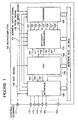
- FIG. 1 there is shown a block diagram of a first embodiment of the microcomputer in accordance with the present invention.
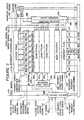
- Figure 2 shows a block diagram of the interrupt controller incorporated in the microcomputer shown in Figure 1
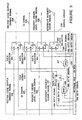
- Figure 3 shows a block diagram of the switch circuit incorporated in the interrupt controller shown in Figure 2.
- a microcomputer generally designated by Reference Numeral 100, is mainly constituted of a CPU 150, an interrupt controller 110, peripheral hardware 120, an I/O (input/output) interface 130 for transferring data between the microcomputer 100 and external devices, and external terminals 170 to 174 and 180 to 195.
- the CPU 150, the interrupt controller 110, the peripheral hardware 120, the I/O interface 130 are coupled to one another through a 16-bit internal address/data multiplexed bus 160 (called an "internal bus” hereinafter) composed of bit "0" to bit "15".
- the CPU 150 supplies to the I/O interface 130 with an internal address latch enable signal 151 indicating that an address is outputted on the internal bus 160, a read signal 152 for reading out data to the internal bus 160 and a write signal 153 for writing the data outputted on the internal bus 160.
- the signal 151 will be called simply an "address latch signal” hereinafter.
- the I/O interface 130 outputs an address latch signal 131, a read signal 132 and a write signal 133 to the interrupt controller 110 and the peripheral hardware 120.
- the external terminal 171 is connected to the I/O interface 130, the CPU 150 and the interrupt controller 110 so as to supply a test signal 175 to these circuits.
- the interrupt controller 110 outputs an interrupt processing request signal 111 to the CPU 150 and the I/O interface 130.
- the I/O interface 130 outputs the interrupt processing request signal 111 to the external terminal 170 when the test signal 175 is active.
- the CPU 150 supplies the interrupt controller 110 with a vector code output enable signal 154 for requesting an output of a vector code, an interrupt enable signal EI 155 indicating that the CPU 150 is in a condition capable of accepting or acknowledging an interrupt request, an interrupt request clear signal 157 for clearing an acknowledged interrupt request after the interrupt request from the interrupt controller 110 is acknowledged, and a priority order level clear signal 156 for clearing the priority order level of the acknowledged interrupt request when a processing for the acknowledged interrupt is terminated.
- the peripheral hardware 120 generates interrupt request signals 121 to 128 which request the CPU to perform a data transfer or a data writing. These interrupt request signals 121 to 128 are supplied to the interrupt controller 110.
- the interrupt controller 110 includes a switch circuit 200 controlled by the test signal 175 so as to select either the vector code output enable signal 154, the EI signal 155, the priority order level clear signal 156 and the interrupt request clear signal 157 or test data outputted on the internal bus 160 and to output the selected signals as an internal vector code output enable signal 204, an internal EI signal 205, an internal priority order level clear signal 206 and an internal interrupt request clear signal 207.
- the interrupt controller 110 also includes an interrupt flag 210 provided to correspond to the interrupt request signals 121 to 128, respectively, and to store generation of the interrupt request, and a mask register 220 provided for each of the interrupt request sources for inhibiting generation of the interrupt request.
- the interrupt controller 110 includes a level "0" flag 230, a level “1” flag 231 and a level “2" flag 232 for designating the level of priority of each interrupt request source.
- the flags are connected to a level hold register 240 for holding a priority order level of an interrupt request that is currently acknowledged by the CPU.
- the flags 230 to 232 output acknowledge request signals 251 to 258 for requesting an interrupt for only interrupt requests having a priority order level higher than the priority order level that is currently acknowledged.
- the interrupt flag 210, the mask register 220, the level flags 230 to 232 are coupled to the internal bus so that these flags and register can be read, written and modified through the internal bus 160.
- the acknowledge request signals 251 to 258 are supplied to a priority order arbitration circuit 260 provided for arbitrating among the interrupt requests having the same priority order level and for generating a request acceptance signal 261 to 268 indicating which of the interrupt requests is selected as the result of arbitration.
- the interrupt controller 110 further includes a vector table 270 storing a vector code of each of the interrupt request sources, and controlled by the priority order arbitration circuit 260 so as to output a vector code corresponding to the selected interrupt request.
- a buffer 280 receives the vector code from the vector table 270 so as to output the received vector to the internal bus 160.
- the interrupt controller 110 includes an address latch 290 responding to the address latch signal 131 to latch an address outputted on the internal bus 160, and an address decoder 295 for decoding the address latched in the address latch 290.
- An output of this address decoder 295 is connected through an address line 296 to one input of an OR gate 201, which has the other input connected to receive the vector code output enable signal 204.
- An output of the OR gate 201 is connected to the buffer 280 as a control signal.
- the interrupt flag 210, the mask register 220, the level "0" flag 230, the level “1” flag 231 and the level “2" flag 232 have 8 bits corresponding to the number of the interrupt request sources, respectively.
- the level hold register 240 has a width of 3 bits corresponding to the number of levels of the priority order.
- the switch circuit 200 includes an AND gate 306 receiving a data signal 366 on a bit “6" of the internal bus 160 (called a “bit “6” signal”) and a bit “8” signal 368 of the same internal bus 160 so as to output a logical product signal, and a data latch 301 for latching a bit "5" signal 365 of the internal bus 160 when the output of the AND gate 306 is brought into “1". Furthermore, the switch circuit 200 includes another AND gate 307 receiving the bit "8" signal 368 of the internal bus 160 and the test signal 175 so as to output a logical product signal as a select signal 308.
- a data selector 302 receives the vector code output enable signal 154 and a bit "4" signal 364 of the internal bus 160 and selects either one of the two received signals in accordance with the select signal 308 so as to output the selected signal as the internal vector code output enable signal 204.
- a data selector 303 receives the EI signal 155 and the output of the data latch 301 and selects either one of the two received signals in accordance with the select signal 308 so as to output the selected signal as the internal EI signal 205.
- a data selector 304 receives the priority order level clear signal 156 and a bit "3" signal 363 of the internal bus 160 and selects either one of the two received signals in accordance with the select signal 308 so as to output the selected signal as the internal priority order level clear signal 206.
- a data selector 305 receives the interrupt request clear signal 157 and a bit "2" signal 362 of the internal bus 160 and selects either one of the two received signals in accordance with the select signal 308 so as to output the selected signal as the internal interrupt request clear signal 207.
- interrupt flag 210 when a interrupt request signal 121 to 128 is generated, a corresponding bit of the interrupt flag 210 is brought to "1". In addition, a bit of the interrupt flag 210 cortesponding to an interrupt request acknowledged by the CPU 150 is brought into "0".
- the mask register 220 functions to acknowledge or inhibit generation of the interrupt at the level of the interrupt flag 210.
- a given bit of the mask register 220 is set to "1”
- a corresponding bit of the interrupt flag 210 is inhibited from being brought "1” indicative of generation of the interrupt request
- a given bit of the mask register 220 is set to "0”
- a corresponding bit of the interrupt flag 210 is allowed to be brought "1" indicative of generation of the interrupt request
- the level "0" flag 230 is used for designating a priority order level of each of the interrupt request signals 121 to 128 to a level "0".
- a interrupt request signal corresponding to a bit of the level "0" flag 230 set to “1” is should be understood to have been designated to a priority order level "0".
- level "1" flag 231 and the level “2" flag 232 are used for designating a priority order level “1” and a priority order level “2" for corresponding interrupt request signals, respectively.
- the level hold register 240 is used for hold a priority order level of an acknowledged interrupt request, and operates to fetch a value of a corresponding bit of each of the respective flags when an interrupt request is acknowledged, and to hold the fetched value until an interrupt processing for the acknowledged interrupt request has been completed. After the interrupt processing for the acknowledged interrupt request has been completed, the level hold register 240 clears the held priority order level of that interrupt request.
- the interrupt register 210, the mask register 220, the level "0" flag 230, the level “1” flag 231, the level “2" flag 232, and the level hold register 240 can be written or read through the internal bus 160 under control of the address latch signal 131, the address latch 290, the address decoder 295, the read signal 132 and the write signal 133.
- Each of the acknowledge request signals 251 to 258 is activated so as to request an interrupt, only when the priority order level designated for the corresponding active interrupt request signal 121 to 128 is higher than the priority order level held in the level hold register 240.
- the priority order arbitration circuit 260 operates to accept the acknowledge request signals 251 to 258 if the EI signal 250 is "1", and when two or more of the acknowledge request signals 251 to 258 are "1", it arbitrates among the the acknowledge request signals of "1". In this embodiment, it is assumed that the smaller the interrupt request signal number is, the higher the priority of the interrupt request signal is. Therefore, if the acknowledge request signals 251 and 252 are simultaneously brought to "1", the acknowledge request signal 251 is selected or acknowledged.
- the CPU 150 executes an ordinary program, and the I/O interface 130 outputs the address latch signal 151, the read signal 152 and the write signal 153 as the address latch signal 131, the read signal 132 and the write signal 133, respectively.
- the data selectors 302 to 305 of the interrupt controller 110 select the vector code output enable signal 154, the EI signal 155, the priority order level clear signal 156 and the interrupt request clear signal 157, which are generated by the CPU 150.
- the I/O interface 130 operates to transfer data between the microprocessor and an external device by used of the external terminals 170, 172 to 174 and 180 to 195 excluding the terminal 171.
- peripheral hardware 120 generates an interrupt request signal 121 set to the priority order level "0" in the course of execution of a main routine of a program by the CPU 150 until the interrupt processing request signal 111 is brought to "1".
- a corresponding bit “0" (bit number or place) of the interrupt flag 210 is set to "1" (bit level or value).
- a corresponding bit “0" (bit number) of the mask register 220 is set to "0" (bit level)
- generation of the interrupt of the interrupt flag 210 is allowed, so that the corresponding acknowledge request signal 251 is outputted to the priority order arbitration circuit 260.
- the priority order arbitration circuit 260 accepts the acknowledge request signal 251 and activates the interrupt processing request signal 111 into “1” and also the interrupt acknowledge signal 261 into “1” which is indicates that the acknowledge request signal 251 is acknowledged.
- This interrupt acknowledge signal 261 is supplied to the vector table 270, the level “0” flag 230, the level “1” flag 231, the level “2” flag 232, and the interrupt flag 210.
- the EI signal is of "0"
- the acceptance of the acknowledge request signal 251 is inhibited until the EI signal is brought to "1".
- the vector table 270 responds to the interrupt acknowledge signal 261 to output to the buffer 280 a vector code corresponding to the interrupt request signal 251.
- the CPU 150 detects the activated interrupt processing request signal 111 of "1" outputted from the priority order arbitration circuit 260, the CPU 150 outputs the vector code output enable signal 154 of "1" to the interrupt controller 110 in order to request a vector code required for executing an interrupt processing program.
- the vector code output enable signal 154 of "1” is supplied through the switch circuit 200 to the buffer 280, and therefore, the buffer 280 outputs the vector code to the internal bus 160.
- the vector code output enable signal 154 or 204 is applied to the level hold register 240, so that the level hold register 240 holds the priority order level "0" of the acknowledged interrupt request 121.
- the CPU 150 receives the vector code outputted on the internal bus 160, and outputs the interrupt request clear signal 157 so as to clear the acknowledged interrupt request.
- the interrupt request clear signal 157 is supplied through the switch circuit 200 to the interrupt flag 210, so that the bit of the interrupt flag 210 corresponding to the interrupt acknowledge signal (261 to 268) of "1", namely, the bit "0" of the interrupt flag 210 is cleared.
- the CPU 150 starts to execute an interrupt processing program corresponding to the received vector code.
- the CPU 150 If the CPU 150 has completed execution of the interrupt processing program, the CPU outputs the priority order level clear signal 156 in order to clear the priority order level of the acknowledged interrupt request.
- the priority order level clear signal 156 is supplied through the switch circuit 200 to the level hold register 240, so that the level hold register 240 is reset.
- the interrupt controller has the order of the priority determined by the hardware (called “default order of priority"). This corresponds to the order of priority determined within the priority order arbitration circuit 260. Namely, as mentioned hereinbefore, when two or more of the acknowledge request signals 251 to 258 are concurrently generated, one of the concurrently generated acknowledge request signals is selected and acknowledged by the the priority order arbitration circuit 260 in accordance with the "default order of priority".
- a method for designating the order of priority about the interrupt request signal 121 will be explained:
- a corresponding bit “0" (bit number or place) of the level “0" flag 230 is set to "1" (bit level or value). If it is desired to set the order of priority for the interrupt request signal 121 to "1”, a corresponding bit “0" (bit number) of the level “1” flag 231 is set to "1" (bit level), or if it is desired to set the order of priority for the interrupt request signal 121 to "2", a corresponding bit “0” (bit number) of the level “2” flag 232 is set to "1” (bit level).
- the priority order for the other interrupt request signals 122 to 128 can be set to any level of the level "0" to the level "2".
- the corresponding bit "0" of the interrupt flag 210 is set to "1". Furthermore, the priority order level of the interrupt request signal 121 set in the level “0" flag 230 to the level “2" flag 232 are compared with the value of the level hold register 240 which holds the priority order level of the currently acknowledged interrupt request. If the priority order level of the interrupt request signal 121 is higher than the value of the level hold register 240, the acknowledge request signal 251 of "1" is outputted to the priority order arbitration circuit 260.
- the interrupt request signal 121 designated to the priority order level "0" is generated, since the priority order level of the interrupt request signal 121 is higher than the priority order level "1" held in the level hold register 240, the acknowledge request signal 251 of "1" is outputted to the priority order arbitration circuit 260.
- the priority order arbitration circuit 260 brings the interrupt processing request signal 111 to "1".
- the CPU 150 reserves the execution of an instruction of the interrupt processing program corresponding to the interrupt request signal 122, and then, starts to execute an interrupt processing program corresponding to the interrupt request signal 121.
- the level hold register 240 holds the priority order level "1" of the interrupt request signal 122 and the priority order level "0" of the interrupt request signal 121.
- a user can controls the priority order level for each of the interrupt request processings, by setting the level "0" flag 230 to the level "2" flag 232.
- test signal 175 If the test signal 175 is brought to "1", the CPU 150 stops execution of the program, and releases the internal bus 160 to the interrupt controller 110, the peripheral hardware 120 and the I/O interface 130.
- the I/O interface 130 outputs, as the address latch signal 131, the read signal 132 and the write signal 133, values supplied to the external terminals 172, 173 and 174. In addition, the I/O interface 130 outputs values inputted to the external terminals 188 to 195 to bits “8" to "15" of the internal bus 150. Furthermore, when "0" is inputted to the external terminal 173, namely, when the read signal 132 is inactive, values applied to the external terminals 180 to 187 are outputted through the I/O interface 130 to bits "0" to "7" of the internal bus 160.
- the address decoder 295 of the interrupt controller 110 decodes an address for the buffer 280
- the address decoder 295 activates the output address line 296 to "1", so that the buffer 280 outputs the vector code to the internal bus 160.
- the select signal 308 is generated in the switch circuit 200, so that the bit "4" signal 364, the output of the data latch 301, the bit “3" signal 363 and the bit “2” signal 362 are outputted as the internal vector output enable signal 204, the internal EI signal 205, the internal priority order level clear signal 205 and the internal interrupt request clear signal 207, respectively.
- the data latch 301 operates to latch the bit "5" of the internal bus 160 when both the bit "8" signal 368 and the bit “7” signal 366 of the internal bus 160 are "1".
- the bit “8" signal 368 of the internal bus 160 is influenced by the values on the bits “0" to "7" of the internal bus 160 which are used when the internal registers of the interrupt controller 110 are read and written. Therefore, it is possible to control the internal vector output enable signal 204, the internal EI signal 205, the internal priority order level clear signal 205 and the internal interrupt request clear signal 207, on the basis of the values applied onto the external terminals 182 to 188.
- the interrupt flag 210, the mask register 220, the priority level hold register 240 and the priority level designation flags 230 t0 232 can be read and written through the external terminals under the function of the switch circuit and under control of the address latch signal 131, the read signal 132 and the write signal 132 supplied from the external terminals 172 to 174 to the interrupt controller 110 without intermediary of the CPU 150. Therefore, contents of the interrupt flag 210 and the priority level designation flags 230 to 232 can be modified through the internal bus from the external terminals
- test mode signal 175 when the test mode signal 175 is active, the vector code outputted from the buffer 280 is read through the internal bus 160 to the external terminals. Furthermore, a signal indicative of the priority order level of the interrupt request currently acknowledged by the CPU is written to the level hold register 240 through the internal bus from the external terminals.
- test for the interrupt controller 110 is performed as follows:
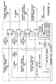
- FIG 4 there is shown a block diagram of a modified example of the switch circuit incorporated in the interrupt controller shown in Figure 2.
- the switch circuit shown in Figure 4 is the same the switch circuit shown in Figure 2, except that a bit "9" signal 369 of the internal bus 160 is applied directly to the data selector 303, so that the internal EI signal 205 is directly controlled by a value applied to the external terminal 189.
- the microcomputer in accordance with the present invention including therein the interrupt controller is such that when the interrupt controller is tested, it is possible to input and output, from and to the external terminals by means of the switch circuit, the address latch signal, the read signal, the write signal, and various control signals outputted on the internal bus and from the CPU. Therefore, the microcomputer in accordance with the present invention is advantageous over the conventional microcomputer in the following points:
- the microcomputer in accordance with the present invention including therein the interrupt controller can be tested for a shortened time, and can also make it possible to efficiently prepare a required test pattern having a high defect detection rate. Therefore, the microcomputer can be inexpensively prepared.
Landscapes
- Engineering & Computer Science (AREA)
- Computer Hardware Design (AREA)
- Theoretical Computer Science (AREA)
- General Engineering & Computer Science (AREA)
- Physics & Mathematics (AREA)
- General Physics & Mathematics (AREA)
- Microelectronics & Electronic Packaging (AREA)
- Quality & Reliability (AREA)
- Microcomputers (AREA)
- Bus Control (AREA)
- Test And Diagnosis Of Digital Computers (AREA)
Applications Claiming Priority (2)
| Application Number | Priority Date | Filing Date | Title |
|---|---|---|---|
| JP1246704A JP2591181B2 (ja) | 1989-09-22 | 1989-09-22 | マイクロコンピュータ |
| JP246704/89 | 1989-09-22 |
Publications (3)
| Publication Number | Publication Date |
|---|---|
| EP0418932A2 true EP0418932A2 (fr) | 1991-03-27 |
| EP0418932A3 EP0418932A3 (en) | 1992-01-02 |
| EP0418932B1 EP0418932B1 (fr) | 1996-07-31 |
Family
ID=17152395
Family Applications (1)
| Application Number | Title | Priority Date | Filing Date |
|---|---|---|---|
| EP90118350A Expired - Lifetime EP0418932B1 (fr) | 1989-09-22 | 1990-09-24 | Micro-ordinateur avec appareil de commande d'interruption à faculté de test simple |
Country Status (4)
| Country | Link |
|---|---|
| US (1) | US5193195A (fr) |
| EP (1) | EP0418932B1 (fr) |
| JP (1) | JP2591181B2 (fr) |
| DE (1) | DE69027963D1 (fr) |
Cited By (4)
| Publication number | Priority date | Publication date | Assignee | Title |
|---|---|---|---|---|
| WO1997044734A1 (fr) * | 1996-05-17 | 1997-11-27 | Advanced Micro Devices, Inc. | Systeme et procede pour tester et mettre au point un controleur d'interruption a multiprocesseur |
| GB2381890A (en) * | 2001-11-12 | 2003-05-14 | Mentor Graphics | Testing interrupts having a service priority order by applying different interrupt priority levels |
| GB2381891A (en) * | 2001-11-12 | 2003-05-14 | Mentor Graphics | Testing interrupts having a service priority order by applying combinations of interrupt priority levels |
| WO2009127902A1 (fr) * | 2008-04-15 | 2009-10-22 | Freescale Semiconductor, Inc. | Dispositif microcontrôleur, dispositif de débogage de microcontrôleur, procédé de débogage d'un dispositif microcontrôleur et ensemble microcontrôleur |
Families Citing this family (13)
| Publication number | Priority date | Publication date | Assignee | Title |
|---|---|---|---|---|
| FR2680591B1 (fr) * | 1991-08-22 | 1996-01-26 | Telemecanique | Controleur d'interruption programmable, systeme interruptif et procede de controle d'interruption. |
| US5412782A (en) | 1992-07-02 | 1995-05-02 | 3Com Corporation | Programmed I/O ethernet adapter with early interrupts for accelerating data transfer |
| US5530874A (en) * | 1993-02-02 | 1996-06-25 | 3Com Corporation | Network adapter with an indication signal mask and an interrupt signal mask |
| US5428770A (en) * | 1993-08-31 | 1995-06-27 | Motorola, Inc. | Single-chip microcontroller with efficient peripheral testability |
| JPH0877035A (ja) * | 1994-09-06 | 1996-03-22 | Toshiba Corp | 中央処理装置及びマイクロコンピュータ |
| US5535420A (en) * | 1994-12-14 | 1996-07-09 | Intel Corporation | Method and apparatus for interrupt signaling in a computer system |
| US5592674A (en) * | 1994-12-20 | 1997-01-07 | International Business Machines Corporation | Automatic verification of external interrupts |
| KR0156173B1 (ko) * | 1995-11-21 | 1998-11-16 | 문정환 | 인터럽트 발생회로 |
| US5734910A (en) * | 1995-12-22 | 1998-03-31 | International Business Machines Corporation | Integrating multi-modal synchronous interrupt handlers for computer system |
| US6370596B1 (en) * | 1999-08-03 | 2002-04-09 | Chameleon Systems, Inc. | Logic flag registers for monitoring processing system events |
| US6993685B2 (en) * | 2002-09-12 | 2006-01-31 | Hewlett-Packard Development Company, L.P. | Technique for testing processor interrupt logic |
| US8490107B2 (en) | 2011-08-08 | 2013-07-16 | Arm Limited | Processing resource allocation within an integrated circuit supporting transaction requests of different priority levels |
| JP6266239B2 (ja) | 2013-07-11 | 2018-01-24 | ルネサスエレクトロニクス株式会社 | マイクロコンピュータ |
Family Cites Families (9)
| Publication number | Priority date | Publication date | Assignee | Title |
|---|---|---|---|---|
| US4004283A (en) * | 1974-10-30 | 1977-01-18 | Motorola, Inc. | Multiple interrupt microprocessor system |
| US4124888A (en) * | 1975-12-24 | 1978-11-07 | Computer Automation, Inc. | Peripheral-unit controller apparatus |
| US4438492A (en) * | 1980-08-01 | 1984-03-20 | Advanced Micro Devices, Inc. | Interruptable microprogram controller for microcomputer systems |
| JPS58134338A (ja) * | 1982-02-05 | 1983-08-10 | Fuji Electric Co Ltd | デイジタル計算機の制御方式 |
| US4648029A (en) * | 1984-08-27 | 1987-03-03 | International Business Machines Corporation | Multiplexed interrupt/DMA request arbitration apparatus and method |
| US4716523A (en) * | 1985-06-14 | 1987-12-29 | International Business Machines Corporation | Multiple port integrated DMA and interrupt controller and arbitrator |
| JPS63310035A (ja) * | 1987-06-11 | 1988-12-19 | Mitsubishi Electric Corp | マイクロコンピユ−タ |
| JPS6478329A (en) * | 1987-09-19 | 1989-03-23 | Fujitsu Ltd | Interruption controller |
| US5101497A (en) * | 1988-09-09 | 1992-03-31 | Compaq Computer Corporation | Programmable interrupt controller |
-
1989
- 1989-09-22 JP JP1246704A patent/JP2591181B2/ja not_active Expired - Fee Related
-
1990
- 1990-09-21 US US07/586,789 patent/US5193195A/en not_active Expired - Fee Related
- 1990-09-24 DE DE69027963T patent/DE69027963D1/de not_active Expired - Lifetime
- 1990-09-24 EP EP90118350A patent/EP0418932B1/fr not_active Expired - Lifetime
Cited By (7)
| Publication number | Priority date | Publication date | Assignee | Title |
|---|---|---|---|---|
| WO1997044734A1 (fr) * | 1996-05-17 | 1997-11-27 | Advanced Micro Devices, Inc. | Systeme et procede pour tester et mettre au point un controleur d'interruption a multiprocesseur |
| GB2381890A (en) * | 2001-11-12 | 2003-05-14 | Mentor Graphics | Testing interrupts having a service priority order by applying different interrupt priority levels |
| GB2381891A (en) * | 2001-11-12 | 2003-05-14 | Mentor Graphics | Testing interrupts having a service priority order by applying combinations of interrupt priority levels |
| GB2381891B (en) * | 2001-11-12 | 2003-10-29 | Mentor Graphics | Testing the interrupt priority levels in a microprocessor |
| GB2381890B (en) * | 2001-11-12 | 2003-10-29 | Mentor Graphics | Testing the interrupt sources of a microprocessor |
| WO2009127902A1 (fr) * | 2008-04-15 | 2009-10-22 | Freescale Semiconductor, Inc. | Dispositif microcontrôleur, dispositif de débogage de microcontrôleur, procédé de débogage d'un dispositif microcontrôleur et ensemble microcontrôleur |
| US8464098B2 (en) | 2008-04-15 | 2013-06-11 | Freescale Semiconductor, Inc. | Microcontroller device, microcontroller debugging device, method of debugging a microcontroller device, microcontroller kit |
Also Published As
| Publication number | Publication date |
|---|---|
| JP2591181B2 (ja) | 1997-03-19 |
| US5193195A (en) | 1993-03-09 |
| JPH03109644A (ja) | 1991-05-09 |
| DE69027963D1 (de) | 1996-09-05 |
| EP0418932A3 (en) | 1992-01-02 |
| EP0418932B1 (fr) | 1996-07-31 |
Similar Documents
| Publication | Publication Date | Title |
|---|---|---|
| US5193195A (en) | Microcomputer having easily testable interrupt controller | |
| EP0127440B1 (fr) | Dispositif de circuit intégré incorporant une unité de traitement de données et une ROM mémorisant des programmes d'application | |
| EP0165517A2 (fr) | Emulateur pour dispositifs VLSI à ensemble d'instructions non-fixé | |
| EP0702297B1 (fr) | Processeur des données avec circuit de point d'arrêt | |
| EP1324190A2 (fr) | Système de traitement de données avec unité de lecture-modification-écriture | |
| EP0443557B1 (fr) | Appareil de commande d'interruption capable de réaliser la fonction d'encastrement d'interruption | |
| US5168559A (en) | Emulation system capable of complying with microcomputers having different on-chip memory capacities | |
| JPH0332818B2 (fr) | ||
| JPH02224140A (ja) | 割込試験装置 | |
| US6842812B1 (en) | Event handling | |
| US5287522A (en) | External procedure invocation apparatus utilizing internal branch vector interrupts and vector address generation, in a RISC chip | |
| JPH11282709A (ja) | インサーキットエミュレータ | |
| US5761482A (en) | Emulation apparatus | |
| KR100223096B1 (ko) | 내부 메모리 맵 레지스터를 관측하는 방법 및 장치 | |
| EP0840221B1 (fr) | Micro-ordinateur à bus de paquets | |
| US7237099B2 (en) | Multiprocessor system having a plurality of control programs stored in a continuous range of addresses of a common memory and having identification registers each corresponding to a processor and containing data used in deriving a starting address of a CPU-linked interrupt handler program to be executed by the corresponding processor | |
| US5500830A (en) | Memory access device | |
| US7765383B2 (en) | Data processing unit and data processing apparatus using data processing unit | |
| JP3077807B2 (ja) | マイクロコンピュータシステム | |
| JPH06230985A (ja) | タスク制御回路、及びマイクロプロセッサ | |
| JPH1040130A (ja) | マイクロコンピュータ | |
| US6658514B1 (en) | Interrupt and control packets for a microcomputer | |
| JP2558902B2 (ja) | 半導体集積回路装置 | |
| JPS59123933A (ja) | アドレス比較方式 | |
| JPH09106359A (ja) | 半導体集積回路 |
Legal Events
| Date | Code | Title | Description |
|---|---|---|---|
| PUAI | Public reference made under article 153(3) epc to a published international application that has entered the european phase |
Free format text: ORIGINAL CODE: 0009012 |
|
| 17P | Request for examination filed |
Effective date: 19901004 |
|
| AK | Designated contracting states |
Kind code of ref document: A2 Designated state(s): DE FR GB |
|
| PUAL | Search report despatched |
Free format text: ORIGINAL CODE: 0009013 |
|
| AK | Designated contracting states |
Kind code of ref document: A3 Designated state(s): DE FR GB |
|
| 17Q | First examination report despatched |
Effective date: 19940405 |
|
| GRAA | (expected) grant |
Free format text: ORIGINAL CODE: 0009210 |
|
| AK | Designated contracting states |
Kind code of ref document: B1 Designated state(s): DE FR GB |
|
| PG25 | Lapsed in a contracting state [announced via postgrant information from national office to epo] |
Ref country code: FR Effective date: 19960731 |
|
| GRAH | Despatch of communication of intention to grant a patent |
Free format text: ORIGINAL CODE: EPIDOS IGRA |
|
| REF | Corresponds to: |
Ref document number: 69027963 Country of ref document: DE Date of ref document: 19960905 |
|
| PGFP | Annual fee paid to national office [announced via postgrant information from national office to epo] |
Ref country code: FR Payment date: 19960930 Year of fee payment: 7 |
|
| PG25 | Lapsed in a contracting state [announced via postgrant information from national office to epo] |
Ref country code: GB Effective date: 19961031 |
|
| PG25 | Lapsed in a contracting state [announced via postgrant information from national office to epo] |
Ref country code: DE Effective date: 19961101 |
|
| EN | Fr: translation not filed | ||
| PLBE | No opposition filed within time limit |
Free format text: ORIGINAL CODE: 0009261 |
|
| STAA | Information on the status of an ep patent application or granted ep patent |
Free format text: STATUS: NO OPPOSITION FILED WITHIN TIME LIMIT |
|
| GBPC | Gb: european patent ceased through non-payment of renewal fee |
Effective date: 19961031 |
|
| 26N | No opposition filed |