EP0419184A2 - Méthode et dispositif de commande d'un appareil d'affichage - Google Patents
Méthode et dispositif de commande d'un appareil d'affichage Download PDFInfo
- Publication number
- EP0419184A2 EP0419184A2 EP90310156A EP90310156A EP0419184A2 EP 0419184 A2 EP0419184 A2 EP 0419184A2 EP 90310156 A EP90310156 A EP 90310156A EP 90310156 A EP90310156 A EP 90310156A EP 0419184 A2 EP0419184 A2 EP 0419184A2
- Authority
- EP
- European Patent Office
- Prior art keywords
- display
- data
- side electrodes
- frame
- electrodes
- Prior art date
- Legal status (The legal status is an assumption and is not a legal conclusion. Google has not performed a legal analysis and makes no representation as to the accuracy of the status listed.)
- Granted
Links
- 238000000034 method Methods 0.000 title claims abstract description 20
- 239000011159 matrix material Substances 0.000 claims description 2
- 239000010409 thin film Substances 0.000 description 29
- 238000010586 diagram Methods 0.000 description 23
- 238000010276 construction Methods 0.000 description 13
- 239000000126 substance Substances 0.000 description 4
- 239000003990 capacitor Substances 0.000 description 3
- 239000011521 glass Substances 0.000 description 2
- 238000012986 modification Methods 0.000 description 2
- 230000004048 modification Effects 0.000 description 2
- 239000000758 substrate Substances 0.000 description 2
- 238000006243 chemical reaction Methods 0.000 description 1
- 239000004973 liquid crystal related substance Substances 0.000 description 1
Images


Classifications
-
- G—PHYSICS
- G09—EDUCATION; CRYPTOGRAPHY; DISPLAY; ADVERTISING; SEALS
- G09G—ARRANGEMENTS OR CIRCUITS FOR CONTROL OF INDICATING DEVICES USING STATIC MEANS TO PRESENT VARIABLE INFORMATION
- G09G3/00—Control arrangements or circuits, of interest only in connection with visual indicators other than cathode-ray tubes
- G09G3/20—Control arrangements or circuits, of interest only in connection with visual indicators other than cathode-ray tubes for presentation of an assembly of a number of characters, e.g. a page, by composing the assembly by combination of individual elements arranged in a matrix no fixed position being assigned to or needed to be assigned to the individual characters or partial characters
- G09G3/22—Control arrangements or circuits, of interest only in connection with visual indicators other than cathode-ray tubes for presentation of an assembly of a number of characters, e.g. a page, by composing the assembly by combination of individual elements arranged in a matrix no fixed position being assigned to or needed to be assigned to the individual characters or partial characters using controlled light sources
- G09G3/30—Control arrangements or circuits, of interest only in connection with visual indicators other than cathode-ray tubes for presentation of an assembly of a number of characters, e.g. a page, by composing the assembly by combination of individual elements arranged in a matrix no fixed position being assigned to or needed to be assigned to the individual characters or partial characters using controlled light sources using electroluminescent panels
Definitions
- the present invention generally relates to a display device and more particularly, to a method of driving a display device, for example, a capacitive flat matrix display panel (referred to as a thin film EL display device hereinafter), etc.
- a capacitive flat matrix display panel referred to as a thin film EL display device hereinafter
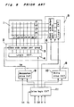
- Fig. 8 is a block diagram showing overall construction of a conventional thin film EL display device, which generally includes a display panel 1, a data side switching circuit 2, a scanning side switching circuit 5, a drive circuit 8, and a drive logic circuit 11 coupled to each other as illustrated.
- the display panel 1 is composed of a thin film EL element.
- this thin film EL element is, for example, of a double insulated type thin film EL element, it includes belt-like transparent electrodes arranged in a parallel relation on a glass substrate, a dielectric substance applied thereover, an EL layer further applied thereover, and another dielectric substance further applied thereon to provide a three-layered structure, and belt-like back electrodes further applied thereover so as to extend parallely in a direction intersecting at right angles with said transparent electrodes referred to above.
- the transparent electrodes of the thin film EL element are set to be the data side electrodes x1 to x8, while the back electrodes of said thin film EL element are adapted to be the scanning side electrodes y1 to y4.
- the data side switching circuit 2 is intended to apply OV or V M as a modulation voltage individually to the respective data side electrodes x1 to x8, and includes a group of data side output ports 3 individually connected to the respective data side electrodes x1 to x8, and a logic circuit 4 which receives display data corresponding to the respective data side electrodes x1 to x8 so as to turn on or off the data side output ports 3 according to said display data.
- the drive circuit 8 is arranged to generate a high voltage for driving the display panel 1 from a predetermined constant reference voltage V D , and is provided with a modulation drive circuit 9 for supplying modulation voltage Vm to the data side output ports 3, and a write drive circuit 10 for supplying write voltages Vw1 and -Vw2 to the scanning side output ports 6.
- the drive logic circuit 11 is a circuit for generating various timing signals necessary for driving the display panel 1, based on input signals such as a display data signal D, a data transfer clock CK, a horizontal synchronizing signal H, and a vertical synchronizing signal V, etc.
- the fundamental driving for the display of the thin film EL display device as described above is effected by applying OV or V M to the data side electrodes x1 to x8 as modulation voltages corresponding to the display data which determine light emission or non-light emission, with a section extending over first and second two frames being set as one period, and also, by applying the write voltage Vw1 to the scanning side electrodes y1 to y4 at the first frame, and the write voltages -Vw2 thereto at the second frame by line sequence.
- a superposing effect or offset effect of the write voltage Vw1 or -Vw2 and the modulation voltage OV or V M is produced at the portions of picture elements where the data side electrodes x1 to x8 and the scanning side electrodes y1 to y4 intersect each other, and a voltage Vw1 higher than a light emitting threshold voltage Vth or a voltage Vw2 lower than the light emitting threshold voltage Vth is applied to each picture element as an effective voltage, whereby the respective picture elements are brought into the light emitting state or non-light emitting state to provide the predetermined display.
- the thin film EL display device as a driving method for varying brightness of the respective picture elements in a plurality of stages, i.e. for effecting gradation display, there have been known an amplitude control system for controlling amplitude of the modulation voltage V M to be impressed to the data side electrodes x1 to x8, a pulse width modulation system for varying pulse width of the modulation voltage V M , and a frequency modulation system for thinning out the display data of either the first frame or second frame.
- an amplitude control system for controlling amplitude of the modulation voltage V M to be impressed to the data side electrodes x1 to x8, a pulse width modulation system for varying pulse width of the modulation voltage V M , and a frequency modulation system for thinning out the display data of either the first frame or second frame.
- the gradation display is to be effected by the driving method of the known frequency modulation system as referred to above, there has also been such a disadvantage that, in the case where the display data is cut in the first frame or in the second frame, the effective voltages to be applied to the picture element is the same in the one period consisting of the first frame and second frame, and after all, the gradations which can be displayed are limited only to three gradations for light emission, non-light emission and intermediate tone, with limitation to the increase in the number of stages for the gradations.
- an object of the present invention is to provide a driving method of a display device, which is so arranged that the number of stages for gradation display may be increased through a simple circuit construction.
- Another object of the present invention is to provide a driving method of a driving device of the above described type, which may be readily effected by the driving device with simple construction.
- a method of driving a display device with a plurality of scanning side electrodes (y1 to y4) and a plurality of data side electrodes (x1 to x8) which are disposed in directions intersecting each other, and a dielectric layer means interposed between said scanning side electrodes and said data side electrodes, and including steps of applying modulation voltages corresponding to display data to said data side electrodes, and also applying writing voltages of positive or negative nature to said scanning side electrodes through line sequence, so as to cause picture elements composed of said dielectric layer means to emit light.
- the driving method further comprises steps of thinning out the display data, and applying a plurality of kinds of modulation voltages different in amplitude according to each frame, thereby to cause the picture elements to effect gradation display of different brightness in multi-stages.
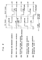
- Fig. 1 a block diagram showing general construction of a thin film EL display device E to which a driving method according to one preferred embodiment of the present invention may be applied.
- the thin film EL display device E has the construction generally similar to the thin film EL display device as described earlier with reference to Fig. 8 for the conventional driving method, and includes a display panel 21, a data side switching circuit 22, a scanning side switching circuit 25, a drive circuit 28, and a drive logic circuit 31 as described hereinafter.
- the display panel 21 is composed of a double insulated type thin film EL element, and includes belt-like transparent electrodes arranged in a parallel relation on a glass substrate, a dielectric substance applied thereover, an El layer further applied thereover, and another dielectric substance further applied thereon to form a three-layered structure, and belt-like back electrodes further applied thereover so as to extend parallely in a direction intersecting at right angles with said transparent electrodes.
- the transparent electrodes of the thin film EL element are set to be the data side electrodes x1 to x8, while the back electrodes of said thin film EL element are adapted to be the scanning side electrodes y1 to y4.
- the data side switching circuit 22 is a circuit intended to apply OV, 1/2V M or V M as a modulation voltage individually to the respective data side electrodes x1 to x8, and includes a group of date side output ports 23 individually connected to the respective data side electrodes x1 to x8, and a logic circuit 24 which receives display data D corresponding to the respective data side electrodes x1 to x8 so as to turn on or off the data side output ports 23 according to said display data D.
- the drive circuit 28 is arranged to generate a high voltage for driving the display panel 21 from a predetermined constant reference voltage V D , and is provided with a modulation drive circuit 29 for supplying a modulation voltage 1/2V M and V M to the data side output ports 23, and a write drive circuit 30 for supplying write voltages Vw1 and -Vw2 to the scanning side output port 26.
- the drive logic circuit 31 is a circuit for generating various timing signals necessary for driving the display panel 21, based on input signals such as display data signals [D1,DO] of 2 bits, a data transfer clock CK, a horizontal synchronizing signal H, and a vertical synchronizing signal V, etc., and includes therein a data processing circuit 32 for processing the above described 2 bit display data signals [D1, DO].
- These 2 bit display data signals [D1,DO] are arranged to correspond so as to designate brightness levels in four gradations as shown in Table 1 below.
- FIG. 2 there is shown circuit construction of the data signal processing circuit 32 referred to above, which includes an AND gate 12 having as two inputs, the lower order bit signal DO of the display data signals [D1, DO] and a frame inversion signal PNF, another AND gate 13 having as two inputs, the higher order bit signal D1 of the display data signal [D1,DO] and signal in which the frame inversion signal PNF is inverted by an invertor 14, and an OR gate 15 connected to outputs of said AND gates 12 and 13 as two inputs, with the output of said OR gate 15 being applied, as the display data D, to the logic circuit 24 of the data side switching circuit 22 of Fig. 1.
- one period for driving is set to be closed by the first frame and second frame, and the above frame inversion signal PNF is applied as the signal which assumes a high level (referred to as H level hereinafter) in the first frame, and a low level (referred to as L level hereinafter) in the second frame.
- H level high level
- L level low level
- a signal MVT for on/off control of said transistor is applied, while, to the gate of the other transistor 18, a signal MVU for on/off control thereof is applied through an AND gate 20, with a PNF signal being applied to the AND gate 20 as the other input thereof.
- the signals MVD and MVU are each pulses having one scanning period as a cycle.
- Fig. 4 is a timing chart showing driving of any desired picture elements for the thin film EL display device of Fig. 1, in which Fig. 4-(1) shows the waveform diagram of writing voltage to be applied to the scanning side electrodes, Fig. 4-(2) represents the waveform diagram of modulation voltage to be applied to the data side electrodes, Fig. 4-(3) indicates the waveform diagram of effective voltage of the display of brightness levels at 0 and 3, Fig. 4-(4) denotes the waveform diagram of effective voltage during driving of the display of brightness level 2 (i.e. higher side brightness of the intermediate tone), and Fig. 4-(5) shows the waveform diagram of effective voltage during driving of the display of brightness level 1 (i.e. lower side brightness of the intermediate tone).
- Fig. 5 is a timing chart representing driving of the modulation driving circuit 29 referred to earlier, in which Fig. 5-(1) shows the waveform diagram for the MVD signal, Fig. 5-(2) denotes the waveform diagram for the PNF signal, Fig. 5-(3) represents the waveform diagram for the MVU signal, Fig. 5-(4) indicates the waveform diagram of the output signal of the AND gate 20, and Fig. 5-(5) shows the waveform diagram of the modulation voltage to be outputted from the modulation drive circuit 29 respectively.
- OV or V M is applied as the modulation voltage in the first frame, while OV or 1/2V m is impressed in the second frame.
- the modulation voltage V M in the first frame, and the modulation voltage 1/2V M in the second frame are supplied from the modulation drive circuit 29 in the manner as described hereinafter.
- the MVD signal becomes "High” to turn on the transistor 17, and therefore, the capacitor 19 is charged by an amount equivalent to 1/2V M (Fig. 3).
- the MVD signal becomes "Low”, while the MVD signal becomes "High” as shown in Fig. 5-(3).
- the output of the AND gate 20 becomes "High” as shown in Fig. 5-(4), and the transistor 18 is turned on, with the potential of the capacitor 19 at the side of the junction between the transistors 17 and 18 becomes 1/2 V M , and at this time, the output of the modulation drive circuit 29 becomes V M as represented in Fig. 5-(5).
- the 2 bit display data signal [D1,DO] to be inputted is converted into the 1 bit display data D in the manner as described hereinbelow.
- the display data signals [Dl,DO] are of [H,L] equivalent to the brightness level 1 (lower side brightness in the intermediate tone)
- the output of the AND gate 12 becomes “Low” level both in the first frame and the second frame
- the output of the AND gate 13 becomes “High” level only in the second frame
- the display data D becomes "Low” level in the first frame, and "high” level in the second frame as shown in Table 1.
- the display data signals [D1,DO] are of [L,H] corresponding to the brightness level 2 (i.e.
- the output of the AND gate 12 becomes “High” level only in the first frame, while output of the AND gate 13 becomes “Low” level both in the first frame and second frame, and accordingly, the display data D becomes "High” level in the first frame, and "Low” level in the second frame as shown in Table 1.
- the display data signals [D1,DO] are of [H,H] equivalent to the brightness level 3 (total light emissions
- the output of the AND gate 12 becomes “High” level only in the first frame
- the output of the AND gate 13 becomes “High” level only in the second frame
- the display data D becomes "High” level both in the first and second frames as shown in Table 1.
- on/off state of the group of data side output ports 23 is controlled according to the display data D. More specifically, in the first frame, when the display data D is of "High” level, OV is selected as the modulation voltage to be applied to the data side electrodes x1 to x8 (shown in the solid line in Fig. 4-(2)), and when the display data D is of "Low” level, V M is selected as the modulation voltage (shown in the dotted line in Fig. 4-(2)).
- the modulation voltage corresponding to the case where the display data D shown in the dotted line in Fig. 4-(2) is of "Low” level is a modulation voltage which acts to offset the writing voltages Vw1 and -Vw2 shown in Fig. 4-(1), and corresponds to the non-light emission in the case of 01 display (two stage display for light emission or non-light emissions.
- the modulation voltage corresponding to the case where the display data D shown in the solid line in Fig. 4-(2) is of "High” level is a modulation voltage which acts to be superposed on the writing voltages Vwl and -Vw2, and corresponds to the light emission in the case of 01 display.
- the effective voltage to be applied to the picture elements is equivalent to the difference between the writing voltages Vwl and -Vw2 (Fig. 4-(1)) to be applied to the scanning side electrodes corresponding to the picture elements and the modulation voltages OV, 1/2V M and V M to be applied to the data side electrodes corresponding to said picture elements, and represented by the waveform shown in Fig. 4-(3).
- the polarities of the effective voltage are given based on the data side electrodes as the reference).
- the solid line represents the case of the brightness level 3 (total light emissions, while the dotted line shows the case of the brightness level 0 (non-light emission).
- display driving equivalent to that in which the display data signals [D1,DO] for the total light emission are cut at the second frame is to be effected.
- the display data D is of "Low” level (accordingly, the modulation voltage is V M ) in the first frame, and is of "High” level (accordingly, the modulation voltage is 1/2V M ) in the second frame, and therefore, the effective voltage becomes the voltage Vw2 corresponding to the non-light emission in the first frame, and the voltage -(Vw2+1/2V M ) corresponding to the total light emission in the second frame as shown in Fig. 4-(5).
- display driving equal to that in which the display data signals [D1,D0] for the total light emission are cut in the first frame, is to be effected.
- the effective voltage to be impressed to the picture elements in one period in which the first and second frames are combined becomes larger in the case of the display for the brightness level 2 than in the case of the display for the brightness level 1.
- the intermediate tone is to be displayed in two stages, thus effecting the display in four gradations on the whole.
- the present invention is not limited in its application to the above alone, but may be so modified, for example, as to effect the display in three stages of non-light emission, intermediate tone, and total light emission through employment of the same display device.
- Fig. 6 is a timing chart showing driving of any desired picture element in the case of the display of the three gradations referred to above, in which Fig. 6-(1) shows the waveform diagram of writing voltage to be applied to the scanning side electrodes, Fig. 6-(2) represents the waveform diagram of modulation voltage to be applied to the data side electrodes, Fig. 6-(3) indicates the waveform diagram of effective voltage to be applied to the picture elements during driving of the display for the non-light emission and total light emission, Figs. 6-(4) and 6-(5) denote the waveform diagrams of effective voltages during driving of the display of the intermediate tone.
- Fig. 7 is a timing chart representing driving of the modulation driving circuit 29 in the case of the above three gradation display, in which Fig. 7-(1) shows the waveform diagram for the MVU signal, Fig. 7-(2) represents the waveform diagram for the MVU signal, and Fig. 7-(3) shows the waveform diagram of the modulation voltage to be outputted from the modulation drive circuit 29 respectively.
- the writing voltage -Vw2 is applied in the second frame in the similar manner as in the four gradation display described earlier.
- V M is applied as the modulation voltage (similarly both in the first and second frames).
- This modulation voltage V M is supplied from the modulation drive circuit 29 in the manner as described hereinafter.
- the MVD signal becomes "High level
- the MVU signal becomes "High, in the similar manner as in the four gradation display.
- the AND gate 20 instead of the PNF signal, the signal assuming "High” level all through the first and second frames is applied. Accordingly, the output of the AND gate 20 becomes equal to the MVU signal through the first and second frames, and the transistor 18 is turned on per each scanning period in any of the frames, and thus, one kind of modulation voltage VH is outputted from the modulation drive circuit 29 per each scanning period as shown in Fig. 7-(3).
- the display data signals [D1,DO] are set to either of the state of brightness level 1 or 2 in the case of the four gradation display, as the signals corresponding to the intermediate tone (Any of such states is acceptable).
- on/off state of the group of data side output ports 23 is controlled in the similar manner as in the four gradation display according to the display data D applied from the data signal processing circuit 32. More specifically, in the first frame, when the display data D is of "High” level, OV is selected as the modulation voltage to be applied to the data side electrodes x1 to x8 (shown in the solid line in Fig. 6-(2)), and when the display data D is of "Low” level, V M is selected as the modulation voltage (shown in the dotted line in Fig. 6-(2)).
- V M is selected as the modulation voltage (shown in the solid line in Fig. 6-(2))
- OV is selected as the modulation voltage (shown in the dotted line in Fig. 6-(2)).
- the effective voltage to be impressed to the picture elements takes the form as shown in the solid line in Fig. 6(3) (corresponding to the modulation voltage shown in the solid line in Fig. 6-(2)) in the case of the total light emission display, while it takes the form as shown in the dotted line in Fig. 6-(3) (corresponding to the modulation voltage shown in the dotted line in Fig. 6-(2)) in the case of non-light emission display.
- display driving equivalent to that in which the display data signals [D1,DO] for the whole light emission are cut at the second frame is to be effected.
- display driving equal to that in which the display data signal [D1,DO] for the total light emission are cut in the first frame, is to be effected.
- the effective voltage to be impressed to the picture elements in one period in which the first and second frames are combined becomes equal in any of the intermediate tone display, and thus, the three gradation display for the non-light emission, intermediate tone, and total light emission is to be effected.
- the driving method of the present invention is described with reference to the case of the gradation display by the thin film EL display device, the concept of the present invention is not limited in its application to such thin film EL display device alone, but may be readily applied to other display devices, for example, to a liquid crystal display device and the like as well.
- gradation display in more than three stages may be effected through a simple circuit construction.
Landscapes
- Engineering & Computer Science (AREA)
- Physics & Mathematics (AREA)
- Computer Hardware Design (AREA)
- General Physics & Mathematics (AREA)
- Theoretical Computer Science (AREA)
- Control Of El Displays (AREA)
- Control Of Indicators Other Than Cathode Ray Tubes (AREA)
- Liquid Crystal Display Device Control (AREA)
Applications Claiming Priority (2)
| Application Number | Priority Date | Filing Date | Title |
|---|---|---|---|
| JP240395/89 | 1989-09-16 | ||
| JP1240395A JP2628760B2 (ja) | 1989-09-16 | 1989-09-16 | 表示装置の駆動装置 |
Publications (3)
| Publication Number | Publication Date |
|---|---|
| EP0419184A2 true EP0419184A2 (fr) | 1991-03-27 |
| EP0419184A3 EP0419184A3 (en) | 1992-04-01 |
| EP0419184B1 EP0419184B1 (fr) | 1996-01-03 |
Family
ID=17058843
Family Applications (1)
| Application Number | Title | Priority Date | Filing Date |
|---|---|---|---|
| EP19900310156 Expired - Lifetime EP0419184B1 (fr) | 1989-09-16 | 1990-09-17 | Méthode et dispositif de commande d'un appareil d'affichage |
Country Status (3)
| Country | Link |
|---|---|
| EP (1) | EP0419184B1 (fr) |
| JP (1) | JP2628760B2 (fr) |
| DE (1) | DE69024574T2 (fr) |
Families Citing this family (1)
| Publication number | Priority date | Publication date | Assignee | Title |
|---|---|---|---|---|
| US10400879B2 (en) | 2016-02-15 | 2019-09-03 | Caterpillar Inc. | One way clutch operation monitoring in torque converter |
Family Cites Families (6)
| Publication number | Priority date | Publication date | Assignee | Title |
|---|---|---|---|---|
| US4775891A (en) * | 1984-08-31 | 1988-10-04 | Casio Computer Co., Ltd. | Image display using liquid crystal display panel |
| JPH0634152B2 (ja) * | 1985-12-17 | 1994-05-02 | シャープ株式会社 | 薄膜el表示装置の駆動回路 |
| DE3724086A1 (de) | 1986-07-22 | 1988-02-04 | Sharp Kk | Treiberschaltung fuer eine duennschichtige elektrolumineszenzanzeige |
| JPS6334593A (ja) * | 1986-07-30 | 1988-02-15 | ホシデン株式会社 | 多階調表示方法 |
| JPS6370893A (ja) * | 1986-09-12 | 1988-03-31 | インタ−ナショナル・ビジネス・マシ−ンズ・コ−ポレ−ション | 多色表示方式 |
| JPH01202792A (ja) * | 1988-02-09 | 1989-08-15 | Matsushita Electric Ind Co Ltd | 表示装置 |
-
1989
- 1989-09-16 JP JP1240395A patent/JP2628760B2/ja not_active Expired - Fee Related
-
1990
- 1990-09-17 DE DE1990624574 patent/DE69024574T2/de not_active Expired - Lifetime
- 1990-09-17 EP EP19900310156 patent/EP0419184B1/fr not_active Expired - Lifetime
Also Published As
| Publication number | Publication date |
|---|---|
| DE69024574T2 (de) | 1996-06-20 |
| EP0419184B1 (fr) | 1996-01-03 |
| EP0419184A3 (en) | 1992-04-01 |
| JP2628760B2 (ja) | 1997-07-09 |
| DE69024574D1 (de) | 1996-02-15 |
| JPH03101789A (ja) | 1991-04-26 |
Similar Documents
| Publication | Publication Date | Title |
|---|---|---|
| US5940057A (en) | Method and apparatus for eliminating crosstalk in active matrix liquid crystal displays | |
| JP3680795B2 (ja) | 電気光学装置の駆動方法、駆動回路及び電気光学装置並びに電子機器 | |
| JP3807322B2 (ja) | 基準電圧発生回路、表示駆動回路、表示装置及び基準電圧発生方法 | |
| JP3807321B2 (ja) | 基準電圧発生回路、表示駆動回路、表示装置及び基準電圧発生方法 | |
| US6118421A (en) | Method and circuit for driving liquid crystal panel | |
| KR20050006084A (ko) | 용량성 부하의 구동 회로 및 구동 방법과, 용량성 부하의구동 회로가 제공된 표시 장치 | |
| US20220005430A1 (en) | Phase modulator and phase modulation method | |
| JPWO2001057837A1 (ja) | 電気光学装置の駆動方法、駆動回路および電気光学装置ならびに電子機器 | |
| US6498595B1 (en) | Active matrix liquid crystal display devices | |
| KR100347065B1 (ko) | 액정표시장치의 구동 시스템 및 액정 패널 구동 방법 | |
| KR0123910B1 (ko) | 표시장치의 구동회로 | |
| US5206631A (en) | Method and apparatus for driving a capacitive flat matrix display panel | |
| US5233340A (en) | Method of driving a display device | |
| JPH07306660A (ja) | 液晶表示装置の階調駆動回路及びその階調駆動方法 | |
| KR20050055913A (ko) | 쉬프트 레지스터 회로 | |
| EP0419184A2 (fr) | Méthode et dispositif de commande d'un appareil d'affichage | |
| JPS63175890A (ja) | アクテイブマトリクス型液晶パネルの駆動方法 | |
| EP0544427B1 (fr) | Circuit de contrÔle pour un système d'affichage avec un circuit d'attaque de source numérique, capable de générer des tensions d'attaque à plusieurs niveaux en partant d'une seule source d'énergie externe | |
| EP0477014B1 (fr) | Dispositif d'affichage avec commande de lumminosité | |
| JP2892540B2 (ja) | 表示装置の駆動装置 | |
| KR20030055379A (ko) | 액정표시장치 및 그의 구동방법 | |
| JP3832156B2 (ja) | 電気光学装置の駆動方法、駆動回路及び電気光学装置並びに電子機器 | |
| JPH1164893A (ja) | 液晶表示パネルおよびその駆動方法 | |
| JP2004163903A (ja) | メモリ回路、表示回路、および表示装置 | |
| JP3931909B2 (ja) | 電気光学装置の駆動方法、駆動回路及び電気光学装置並びに電子機器 |
Legal Events
| Date | Code | Title | Description |
|---|---|---|---|
| PUAI | Public reference made under article 153(3) epc to a published international application that has entered the european phase |
Free format text: ORIGINAL CODE: 0009012 |
|
| 17P | Request for examination filed |
Effective date: 19901214 |
|
| AK | Designated contracting states |
Kind code of ref document: A2 Designated state(s): DE GB |
|
| PUAL | Search report despatched |
Free format text: ORIGINAL CODE: 0009013 |
|
| AK | Designated contracting states |
Kind code of ref document: A3 Designated state(s): DE GB |
|
| 17Q | First examination report despatched |
Effective date: 19940107 |
|
| GRAA | (expected) grant |
Free format text: ORIGINAL CODE: 0009210 |
|
| AK | Designated contracting states |
Kind code of ref document: B1 Designated state(s): DE GB |
|
| REF | Corresponds to: |
Ref document number: 69024574 Country of ref document: DE Date of ref document: 19960215 |
|
| PLBE | No opposition filed within time limit |
Free format text: ORIGINAL CODE: 0009261 |
|
| STAA | Information on the status of an ep patent application or granted ep patent |
Free format text: STATUS: NO OPPOSITION FILED WITHIN TIME LIMIT |
|
| 26N | No opposition filed | ||
| REG | Reference to a national code |
Ref country code: GB Ref legal event code: IF02 |
|
| PGFP | Annual fee paid to national office [announced via postgrant information from national office to epo] |
Ref country code: GB Payment date: 20090916 Year of fee payment: 20 |
|
| PGFP | Annual fee paid to national office [announced via postgrant information from national office to epo] |
Ref country code: DE Payment date: 20090910 Year of fee payment: 20 |
|
| REG | Reference to a national code |
Ref country code: GB Ref legal event code: PE20 Expiry date: 20100916 |
|
| PG25 | Lapsed in a contracting state [announced via postgrant information from national office to epo] |
Ref country code: GB Free format text: LAPSE BECAUSE OF EXPIRATION OF PROTECTION Effective date: 20100916 |
|
| PG25 | Lapsed in a contracting state [announced via postgrant information from national office to epo] |
Ref country code: DE Free format text: LAPSE BECAUSE OF EXPIRATION OF PROTECTION Effective date: 20100917 |