EP0420535A2 - Stromversorgung und Monitor zur Überwachung einer elektrischen Last nach einem Stromausfall - Google Patents
Stromversorgung und Monitor zur Überwachung einer elektrischen Last nach einem Stromausfall Download PDFInfo
- Publication number
- EP0420535A2 EP0420535A2 EP90310403A EP90310403A EP0420535A2 EP 0420535 A2 EP0420535 A2 EP 0420535A2 EP 90310403 A EP90310403 A EP 90310403A EP 90310403 A EP90310403 A EP 90310403A EP 0420535 A2 EP0420535 A2 EP 0420535A2
- Authority
- EP
- European Patent Office
- Prior art keywords
- voltage
- unregulated
- regulated
- supply
- magnitude
- Prior art date
- Legal status (The legal status is an assumption and is not a legal conclusion. Google has not performed a legal analysis and makes no representation as to the accuracy of the status listed.)
- Withdrawn
Links
Images


Classifications
-
- G—PHYSICS
- G01—MEASURING; TESTING
- G01R—MEASURING ELECTRIC VARIABLES; MEASURING MAGNETIC VARIABLES
- G01R21/00—Arrangements for measuring electric power or power factor
- G01R21/133—Arrangements for measuring electric power or power factor by using digital technique
- G01R21/1333—Arrangements for measuring electric power or power factor by using digital technique adapted for special tariff measuring
Definitions
- the present invention relates generally to electrical power outage detection apparatus, and more particularly, to power supplies and power monitors for use with electrical and electronic loads requiring an orderly shutdown in the event of a power outage.
- a pulse initiator provides pulses proportional to electrical energy consumption to an electronic register which accumulates and stores the pulses as data representative of such consumption. This data can then be retrieved periodically by a utility company meter reader and used to bill the consumer.
- the time of use register usually employs its own power supply and a battery back-up system for supplying the necessary bias voltages to the register during the period of a power outage to prevent the loss of data in its volatile memory.
- This type of register usually contains a circuit which detects a power outage or low voltage condition from its power supply for switching in the battery back-up system. When a power outage is detected, the register's micro processor usually goes through an orderly shutdown procedure to place the register in a low power mode whereby battery back-up voltage is provided to only those register circuits necessary for time keeping and the preservation of the meter data; namely the register's clock calendar and its volatile memory.
- the electronic demand register like the time of use register, also usually contains its own power supply for providing the necessary bias voltages to the register circuits. However, unlike the time of use register, the demand register does not have a battery back-up system. Instead, the electronic demand register employs a non-volatile data storage or memory for receiving and storing data from the register's micro processor volatile memory when a power outage is detected by the register. The data is thus preserved during the power outage and can be written back to the volatile memory upon the restoration of power to the demand register's power supply.
- Patent 4,591,782 discloses an electronic demand register which receives pulses proportional to power consumption from a conventional induction type watthour meter.
- the register includes a microprocessor, a volatile memory and a non-volatile memory.
- the register also includes its own power supply, power monitor and power fail detect circuitry for signalling the microprocessor of a power outage.
- the microprocessor Upon the receipt of a power fail detect signal, the microprocessor enters into a read/write cycle to transfer data from its volatile memory to the non-volatile memory. As previously mentioned, it takes a certain period of time to complete the transfer of data into the non-volatile memory.
- the power supply and monitor contains a storage capacitor which stores a sufficient quantity of electrical energy to sustain a regulated DC voltage to the register at its normal value for the period of time required to carry out the transfer of the data into the non-volatile memory.
- the power supply, monitor and storage capacitor can accommodate only a single light load imposed by the demand register.
- the demand register's complexity and cost is increased by the incorporation therein, of the power supply, monitor, storage capacitor and power fail detect and timing circuitry necessary to carry out the aforementioned read/write functions.
- enhanced system performance and manufacturing cost advantages can be realized by removing this complexity from the demand register (including other types of electronic registers and controllable loads) and designing it into a less complex universally useable power supply and monitor which can provide sufficient voltage and current during a power outage to a drive either a single load, such as a demand register, or a plurality of loads.
- Fully electronic watthour meters are directly replacing the conventional induction type watthour meter in certain applications. These electronic watthour meters monitor energy consumption and provide data pulses proportional to energy consumption to an electronic register in a manner similar to the induction type watthour meter.
- An electronic watthour meter unlike the conventional induction type meter, requires a power supply for supplying the proper bias voltages to the meter circuits. These bias voltages can also be used by the circuits in an electronic register which receive pulses representative of energy consumption from the electronic meter.
- loads such as an electronic meter and an electronic register
- An embodiment of the invention seeks to provide an electronic metering system having enhanced operating capabilities and which overcomes the disadvantages of the prior art.
- a further embodiment of the invention seeks to provide an electronic metering system capable of detecting a power outage and sustaining, for a prescribed period of time following a power outage, the levels of voltages used by an electronic meter and an electronic register to carry out an orderly shutdown of the metering system.
- Another embodiment of the invention seeks to provide a power supply and power monitor for supplying a regulated voltage to at least one load and controlling the period of time that the regulated voltage remains at a prescribed level following a power outage to enable an orderly shutdown of the load.
- a still further embodiment of the invention seeks to provide, in an electronic metering system, a power supply and power outage monitor capable of providing operating voltages to an electronic meter and an electronic register and sustaining the operating voltages at a prescribed level for a controlled period of time following a power outage to enable the electronic register to save volatile data in a non-volatile storage.
- One aspect of the present invention provides, in an electronic metering system, a power supply and monitor for providing regulated DC voltages to an electronic meter and an electronic register having a programmable processor for storing data in a non-volatile memory upon the detection of an impending power outage.
- a storage element in the power supply and monitor stores a sufficient quantity of expendable electrical energy to continue operation of the electronic register for a long enough period to complete the writing of data to the non-volatile memory.
- the discharge rate of the storage element is linearly controlled by a current regulator monitor.
- Means is provided to detect a power outage to signal the electronic register to store data into the non-volatile memory and disable at least a portion of the circuitry in the electronic meter to reduce the load on the power supply upon detection of a power outage.
- a power supply and monitor develop, from an AC power source, unregulated and regulated DC voltages.
- the regulated DC voltages are provided to electrical loads to power the electronic circuits therein.
- the unregulated voltage Upon the occurrence of a power outage, the unregulated voltage begins to decay from a first level to a second level.
- a power fail detect signal is generated to signal the loads of an impending power outage and to enable the loads to start an orderly shutdown.
- a storage capacitor stores a sufficient quantity of electrical energy from the unregulated DC voltage to enable the regulated DC voltages to remain at their regulated values long enough for the loads to complete their orderly shutdown.
- the discharge rate of the storage capacitor is controlled by a current regulator which monitors at least one regulated DC voltage.
- the storage capacitor is normally disconnected from the power supply load.
- the current regulator is activated to control the discharge rate of the storage capacitor and regulate the magnitude of the regulated DC voltage at a prescribed level for a period of time sufficiently long to enable the loads to complete their orderly shutdown.
- the invention provides means responsive to the regulated DC voltage passing through a prescribed threshold for resetting or initializing a load prior to the expiration of the above mentioned period of time or at the time of initial power up.
- a method of sustaining the application of a regulated DC voltage to an electrical load such as a microprocessor or other controllable device, following the loss of power from an AC supply by; producing an unregulated DC voltage from electrical energy provided by the AC supply; producing a regulated DC voltage from the unregulated DC voltage; storing in a dischargeable energy storage element, such as a capacitor, a sufficient quantity of electric energy from the unregulated DC voltage to maintain the regulated voltage at a prescribed regulated value for a predetermined period of time following the loss of electrical energy from the AC supply; and monitoring the unregulated DC voltage, and in response to a drop in the magnitude thereof from a first value to a second value, regulating the magnitude of the regulated DC voltage by controlling the rate of discharge of the energy storage element to thereby sustain the unregulated DC voltage at its second value and maintain the regulated DC voltage applied to the electrical load at its prescribed value for the predetermined period of time following the loss of electrical energy from the AC supply.
- a dischargeable energy storage element such as a capacitor
- FIG. 1 there is shown, generally at 10, an electronic metering system which includes a Power Supply and Monitor 12, an Electronic Meter 14 (such as a watthour meter) and an Electronic Register 16, such as a demand register.
- a Power Supply and Monitor 12 an Electronic Meter 14 (such as a watthour meter)
- an Electronic Register 16 such as a demand register.
- the Power Supply and Monitor 12 includes an Unregulated Supply 18 for receiving an AC voltage from an AC Supply 20 (See Fig. 2) via two Conductors 22 and 24 designated UX and N (neutral). Supply 18 rectifies the AC voltage input and produces at its output two unregulated DC voltages (+l6VDC UNREG and -16VDC UNREG) on Conductors 26 and 28 respectively. These voltages are applied to an Energy Storage 30
- the Energy Storage 30 stores electrical energy provided by the 16VDC UNREG voltages and supplies those voltages, via Conductors 32 and 34, to Voltage Regulators 36.
- Regulators 36 In response to the 16VDC UNREG voltages, Regulators 36 produce regulated output voltages 5VDC REG on Conductors 38 and 40.
- a control signal is provided from a current regulator in Regulators 36 to the Energy Storage on a Conductor 42 to control the rate of discharge of the Energy Storage upon the detection of a power outage by the Regulators 36. The development of this control signal and how it functions to control discharge rate of the Energy Storage will later be described.
- the Power Supply and Monitor is shown as also including a Current and Voltage Scaling and Isolation block 44 for isolating the line voltage and line current supplied by AC Supply 20 and scaling down the voltage and current to suitable magnitudes for input to the Electronic Meter 14 via Conductors 46 and 48.
- the Voltage and Current Scaling and Isolation circuits may consist of those types of voltage transformers and current transformers or sensors conventionally used in watthour meters.
- a suitable current sensor for use with an electronic meter is disclosed in European Patent Application 0365216 (11ME210) (USSN 259234, entitled Current Sensors). Such assigned to the assignee of the present invention.
- Such voltage and current transformers are conventionally mounted in the base of a meter and as such are not generally an integral part of the meter power supply.
- the Electronic Watthour Meter 14 of Fig. 1 is generally of a well known, prior art type.
- Representative prior art electronic meters suitable for use in the present invention are disclosed in the following U.S. Patents which are assigned to the assignee of the present invention and which are incorporated herein by reference: 4,535,287; 4,556,843; 4,620,150; 4,754,219; and 4,761,605.
- the Electronic Meter 14 is shown as including a Low Voltage Reset 50, a Power Fail Detect 52, a Low Power Mode Control 54, and a Block 56 designated Other Meter Circuitry.
- Block 56 represents conventional electronic metering circuitry such as the prior art electronic meters disclosed in the last aforementioned patents.
- the Meter Circuits 56 receive analog input signals proportional to line voltage and current via Conductors 46 and 48. During normal operation of the System 10, these signals are repeatedly sampled by the Meter Circuits 56, the samples of which are multiplied together to generate pulses on a Conductor 58 collectively representative of and proportional to electrical energy consumption (eg. watthours, kilowatthours or other measures, such as reactive power). For illustrative purposes, these pulses are shown as watthour pulses on Conductor 58 of Fig. 1.
- the watthour pulses are provided to a data input of a Microprocessor or Computer 60 of the Register 16 where they are stored in well known fashion in the volatile memory of the Processor 60.
- the +5VDC REG voltage on Conductor 38 is provided to the Low Voltage Reset 50, the Power Fail Detect 52, the Low Power Mode Control 54, and to the Electronic Register 16 via Conductors 62, 64, 66 and 68 respectively.
- the -5VDC REG voltage on Conductor 40 is supplied to the Mode Control 54 of the Meter 14.
- Two of these regulated voltages ( 5VDC REG) are provided to the Meter 14 and one (+5VDC REG) to the Register 16 to provide the necessary bias voltages for the operation of the various circuits contained therein.
- the Low Voltage Reset Circuit 50 monitors the ⁇ 5VDC REG voltage to effect the generation of a RESET signal on Conductor 70 for the Processor 60. The manner in which this signal is generated will be subsequently described.
- the Mode Control 54 may comprise a conventional electronic switch (such as a CMOS switch) which, when activated by the PWR FAIL signal, disables, or reduces, the ⁇ 5VDC REG voltages to the Meter Circuitry 56.
- This circuit monitors the +16VDC UNREG voltage provided thereto on Conductor 78.
- the purpose of this circuit is to continuously monitor the magnitude of the +16VDC UNREG voltage signal to detect a power outage of the AC Supply 20.
- the PWR FAIL signal on Conductor 72 signals the Processor 60 to begin an orderly shutdown of the Register 16, whereby the Processor 60 stores the meter data, and other information, from its volatile memory into a Non-Volatile Memory 80.
- the Electronic Register 16 can be of any one of several known prior art type demand registers.
- Register 16 in addition to having the Processor 60 and Non-Volatile Memory 80, also includes a Display 82, such as a liquid crystal display, for displaying metering data and other information which is provided thereto by the processor 60.
- Display 82 such as a liquid crystal display, for displaying metering data and other information which is provided thereto by the processor 60.
- U.S. patent Nos. 4,571,692; 4,594,545; 4,598,248; and 4,620,150 disclose representative electronic demand registers suitable for use with the present invention. The above patents are assigned to the assignee of the present invention.
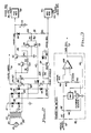
- Fig. 2 is a detailed schematic of the Power Supply and Monitor 12 comprised of the Unregulated Supply 18, Energy Storage 30 and Regulators 36.
- the Power Supply of Fig. 2 is comprised of the Unregulated Supply 18 which is made up of a conventional Power Transformer T1, a conventional bridge rectifier consisting of diodes D1-D4, energy storage and filter capacitors C1 and C2 and Zener diodes D5 and D6. Capacitors C1 and C2 each have typical values of 1000 microfarads. Zener diodes D5 and D6 provide protection for the Power Supply against overvoltage and transients which may occur in the voltage applied to the primary winding of T1 from the AC Supply 20. Zener diodes D5 and D6 are each 22 volt devices, such as a 1N5358A. As shown in Fig.
- the +16VDC UNREG voltage is provided from the Unregulated Supply 18 on Conductor 78 which is connected to the + terminal of C1 and to a Junction 84 of diodes D2 and D4.
- the -16VDC UNREG voltage is provided from the - terminal of C2 on Conductor 28 which is connected to a Junction 86 of diodes D1 and D3.
- Capacitors C1 and C2 are connected in series across the output of the Unregulated Supply 18 and are grounded along with diodes D5 and D6 at a Junction 88.
- capacitor C1 develops a charge across it of approximately +16 volts.
- capacitor C2 develops a charge across it of approximately -16 volts. As a result of these two charges, the total voltage across C1 and C2 is approximately 32 volts.
- the Voltage Regulators 36 are comprised basically of three circuits for regulating the +5VDC REG voltage and two circuits for regulating the -5VDC REG voltage.
- the circuits for regulating the -5VDC REG voltage consists of two voltage regulators, a Negative Pre-regulator, shown generally as 90, providing a -10 VDC REG voltage to a final Negative voltage Regulator 92.
- the Negative Regulator 92 produces the -5VDC REG voltage at its output on Conductor 40.
- the Negative Regulator 92 may be a commercially available voltage regulator, a suitable type being an MC7905 solid state regulator manufactured by Motorola.
- the Negative Pre-regulator 90 consists of a PNP Transistor Q3 (such as a 2N5193) an 11 volt Zener diode D8 (such as a 1N5241B), and a Resistor R6 having a preferred value of 1 Kilohm.
- the emitter of Q3 is connected to the input of the final Negative Regulator 92 and serves to provide the aforementioned -10VDC REG voltage thereto.
- Diode D8 and Resistor R6 are connected in series between ground (at the cathode of D8) and the collector of Q3.
- Base current for controlling the conduction of Q3 is provided by a connection to its base from a Junction 94 between R6 and D8.
- the collector of Q3 is connected to Conductor 28 (34) and receives the -16VDC UNREG voltage from the Unregulated Supply 18.
- the operation of the Negative Pre-regulator 90 is rather conventional and, as such a detailed operational description thereof is not deemed necessary. However, suffice to say, under normal Power Supply operating conditions, the conduction of Q3 is controlled by base current from Junction 94 to accurately regulate the -10VDC REG voltage in response to changes in the magnitude of the -16VDC UNREG voltage.
- the circuit for regulating the +5VDC REG voltage consists of three voltage regulators; (i) a Positive Pre-regulator, shown generally as 96, producing a +9VDC REG voltage, (ii) a final Positive Regulator 98 which receives the +9VDC REG voltage and produces the +5VDC REG voltage at its output on Conductor 38 and (iii) a feedback current or control regulator 99 for providing a feedback control signal for controlling the rate of discharge of a Capacitor 3 in the Energy Storage 30.
- the Positive Regulator 98 may be a commercially available voltage regulator, a suitable type being an LM317 adjustable solid state regulator manufactured by Linear Technology Corporation.
- the Positive Pre-Regulator 96 consists of PNP Transistors Q1 and Q2 (such as a 2N3906 and a 2N5193 respectively), an NPN Transistor Q4 (such as a 2N3904), an 8.2 volt Zener diode D9 (such as a 1N4694), and resistors R1, R2, R3, R4 and R5. Resistors R1-R5 typically have values of 100 Kilohms, 22 Kilohms, 4.7 Kilohms, 1 Kilohm and 22 Kilohms respectively.
- the collector of Q2 is connected to the input of the final Positive Regulator 98 and serves to provide the aforementioned +9VDC REG voltage thereto.
- the emitters of transistors Q1 and Q2 are each connected to the Junction 84 at the output of the Unregulated Supply 18 and receive therefrom, via Conductor 26 (32), the +16VDC UNREG voltage.
- the collector of Q1 is connected to the base of Q2, with that base being connected to one end of resistor R3 having its other end grounded.
- Current for controlling the conduction of transistor Q1 is provided to its base from a Junction 100 between series connected resistors R1 and R2.
- One end of R1 is connected to the emitter of Q1 at the output of the Unregulated Supply 18 on Conductor 26(32).
- One end of resistor R2 is connected to the collector of Q4, the emitter of which is connected to ground at one end of R3.
- Resistor R4 is connected at one end to the base of Q4 and at its other end to a Junction 102 between diode D9 and resistor R5.
- Resistor R5 and diode D9 are connected in series across the +9VDC REG and -10VDC REG voltages at the outputs of the Pre-regulators 90 and 96.
- Diode D9, in conjunction with resistors R4 and R5, serves to provide base current for controlling the conduction of transistors Q4 and Q5.
- This circuit shown generally as 104, is comprised of a diode D7 (such as a 1N4004), a storage cell or capacitor C3 having a preferred value of 1000 microfarads, and a PNP transistor Q5 (such as a 2N3906).
- Diode D9 and resistors R4 and R5 also form elements of the Energy Storage 30, and are shared with the previously described Positive Pre-regulator 96.
- the capacitor C1 also plays a significant role in the operation of the invention and operates as one element of the Energy Storage Circuit 104 to help sustain the +5VDC REG voltage at its prescribed magnitude for a period of time, following a power outage, sufficiently long to enable an orderly shutdown of the Electronic Meter 14 and the Electronic Register 16.
- the storage capacitor C3, along with capacitor C1, has its + terminal connected at the +16VDC UNREG output of the Unregulated Supply 18 as shown at Junction 84 and Conductor 26(32).
- the - terminal of capacitor C3 is connected, via diode D7, to one end of the secondary winding of transformer T1 at a Junction 106 of diodes D3 and D4.
- the - terminal of C3 is also connected, via the control line or Conductor 42, to the collector of transistor Q5.
- a filter capacitor C4 is connected from the +9VDC REG voltage to ground and serves to filter out any ripple in that voltage prior to application to the final Positive Regulator 98.
- Fig. 3 in conjunction with Fig 1, wherein it can be seen that the Power Fail Detect Circuit 52 monitors the +16VDC UNREG voltage on Conductor 78 from the Unregulated Supply 18. As previously described, the Detect Circuit 52 provides a binary 1 PWR FAIL signal, via Conductor 72, to the Processor 60 and the Mode Control 54 upon the occurrence of a power failure in the AC Supply 20.
- the Detect Circuit 52 is a threshold voltage comparator which compares the magnitude of the +16VDC UNREG voltage with a predetermined reference or threshold voltage. As shown in Fig. 3, this reference voltage is provided at the junction of a voltage divider comprised of two resistors R9 and R10 connected between ground and the +5VDC REG voltage on Conductor 64. The ratio of the resistors R9 and R10, in the disclosed embodiment, provide a +2.3VDC reference voltage to the + input terminal of a conventional operational Comparator Amplifier 108.
- the +16VDC UNREG voltage is applied to a - input terminal of Amplifier 108 via a resistor R7.
- Resistor R7 in conjunction with a resistor R8 which is connected between ground and a Junction 112, form a second voltage divider for providing the proper voltage to the - terminal of Amplifier 108.
- the ratio of R7 and R8 are chosen so that the voltage at the - terminal of Amplifier 108 is equal to or greater than the +2.3 VDC reference when the input voltage on Conductor 78 to R7 is +16 volts.
- Resistors R7 and R8 typically have values of 162 Kilohms and 46.4 Kilolims respectively.
- the +16VDC UNREG voltage is at +16 volts.
- the +16VDC UNREG voltage will begin to decay toward zero volts. The manner in which this decay occurs will subsequently be described.
- the voltage at the - input terminal of Amplifier 108 drops to a level (determined by the ratio of R7 and R8 in conjunction with the +2.3 VDC threshold) which causes the output of Amplifier 108 to go from a binary 0 state (0 volts) to a binary 1 state (+5 volts) to thus provide the PWR FAIL signal to the Processor 60 and to the Mode Control 54.
- SW1 When the PWR FAIL signal goes to a binary 1 logic state, that signal is provided, via a Control Line 114, to the input of a normally open conventional switch (such as a CMOS Switch) SW1. In response to the PWR FAIL signal on Line 114, SW1 closes to switch in a Current Source 110. SW1 is connected to the Junction 112 of R7 and R8. Thus, when SW1 closes it applies or injects a prescribed current (referred to as a hysteresis current) into the junction of R7 and R8 which causes the voltage at the junction to decrease by a prescribed amount.
- a hysteresis current a prescribed current
- Current Source 110 may be any suitable device for injecting the proper current, such as a precision current supply or merely a precision resistor connected between SW1 and ground which is switched in parallel with R8 to thus change the ratio of R7 and R8 and allow the voltage at Junction 112 to fall by the proper amount to a prescribed level.
- Reset Circuit 50 is a prior art circuit of known design, the details of which can be found in the aforementioned U.S. patent 4,591,782.
- the Low Voltage Reset 50 is disclosed in Fig. 7 thereof as a Processor Reset Generator 80, and a detailed description of the operation thereof can be found in Column 8, line 62 through 68, and Column 9, lines 1 through 18.
- Patent 4,591,782 is specifically incorporated herein by reference for that detailed description. However, for purposes of clarity and understanding of the present invention, the following operational description of the Low Voltage Reset Circuit 50 will be given.
- the Low Voltage Reset 50 continuously monitors the magnitude of the +5VDC REG voltage provided thereto from the Voltage Regulators 36 via Conductors 38 and 62.
- the voltage on Conductor 62 is at +5VDC and the reset signal on Conductor 70 to the Processor 60 is held low at a binary 0 state (0 volts).
- the +5VDC REG voltage will begin to decay from its nominal +5 volt level toward zero volts.
- the RESET signal on Conductor 70 jumps from approximately zero volts (binary 0 level) to approximately +4 volts (binary 1 level) and then follows the +5VDC REG voltage as it decays further toward zero.
- the Low Voltage Reset 50 will also generate the RESET signal as a pulse on Conductor 70 as the voltage on Conductor 62 passes through the +4 volt threshold level toward the normal regulated +5VDC levels
- Fig. 2 An operational description will now be given, with reference first being made to Fig. 2.
- the system is in normal operation with the AC Supply 20 supplying electrical energy (eg 120VAC) to transformer T1.
- the secondary winding of T1 steps the input voltage down to a proper level for rectification by the Unregulated Supply 18 to generate the ⁇ 16VDC UNREG voltages.
- Capacitors C1 and C2 each develop a charge thereacross of 16 volts to thus produce the +16VDC UNREG voltage on Conductor 26(32) and the -16VDC UNREG voltage on Conductor 28(34).
- Zener diode D9 is an 8.2 volt device, such as a type 1N4694.
- Diode D9 and series connected resistor R5 are connected across the outputs of the Pre-regulators 90 and 96 to thus continuously monitor the +9VDC REG voltage at the cathode of D9.
- D9 continuously operates in its avalanche breakdown region to maintain a substantially constant 8.2 volt voltage drop thereacross, while the current through D9 will vary (increase or decrease) with corresponding changes in the magnitude of the +9VDC REG voltage.
- D9 functions as a current regulator to control the current flowing through R4, R5 and the emitter/base junctions of transistors Q4 and Q5.
- diode D9 operates to sustain a regulated positive voltage (eg. approximately +0.6 to +1.0 volt) at the bases of Q4 and Q5 to cause Q4 to conduct and turn off Q5.
- a regulated positive voltage eg. approximately +0.6 to +1.0 volt
- This voltage at the base of Q4 is controlled by current flowing through R4 and R5 as regulated by D9, and its magnitude at the base of Q4 is a function of the ratio of the voltage drop across the emitter/base junction of Q4 and the total drop across R4 and R5.
- Transistor Q4 normally operates in its linear region as a current regulator.
- the emitter/collector current of Q4 varies in response to small variations in its base voltage to control the voltage at its collector and thus the voltage applied therefrom to resistor R2.
- transistors Q1 and Q2 These two transistors also normally operate in their linear regions and function together to maintain the voltage at the collector of Q2 at +9 volts.
- the base of Q1 is connected at Junction 100 of the voltage divider comprised of R1 and R2.
- the collector of Q1 is connected as a control input for Q2 at its base.
- Resistor R3 serves to provide base bias current for Q2.
- One end of R2, along with the emitter of Q1 is connected to Conductor 26(32) and monitors the +16VDC UNREG voltage.
- a control voltage is provided to one end of R2 from the collector of Q4.
- the conduction of Q4 controls the magnitude of the voltage at Junction 100 at the proper level to control the collector current of Q1 at the proper level to control the conduction of Q2 to regulate and maintain the +9VDC REG voltage at its nominal +9volt level.
- the Positive Regulator 98 receives the +9VDC REG voltage to in turn provide the +5VDC REG voltage to the various circuits in the Meter 14 and the Register 16.
- Diode D7 functions as a half-wave rectifier to charge C3 each time the voltage at the Junction 106 (cathode of D7) goes negative (approximately - 16 volts) with respect to the positive voltage approximately +16VDC UNREG) at Junction 84 on Conductor 26(32). While full-wave charging of C3 can be provided, it has been found that half-wave charging of C3 is more than adequate because there is no load across C3 during normal operation. For a continued detailed operational description and understanding of the Energy Storage 104 and the invention reference is now made to Fig. 5.
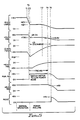
- the +16VDC UNREG, +5VDC REG and -5VDC REG voltages are sustained at their normal levels.
- the levels of these voltages, along with the levels and states of the other key voltages and signals for controlling the operation of the invention are shown in the timing diagram of Fig. 5.
- Fig. 5 Also shown in Fig. 5 is the level of the +5VDC REG voltage applied during normal operation to all of the various circuits of the Electronic Meter 14 and the Electronic Register 16. Of particular interest at this time is the state of the RESET signal on Conductor 70 connecting the Low Voltage Reset 50 to the Processor 60. As can be seen, the RESET signal is at a binary 0 state, or 0 volt level, so long as the +5VDC REG voltage is at +5 volts. During normal system operation, the RESET signal has no affect on the Processor 60.
- Fig. 5 the power outage is shown as occurring at a time T1, at which time capacitors C1 and C2 begin to discharge through the normal load on the Power Supply and Monitor 12 as seen at the outputs of the Positive and Negative Regulators 92 and 98 on Conductors 40 and 38 respectively.
- This discharge is shown at the top of Fig. 5 where the +16VDC UNREG voltage decays from its normal +16 volt level to a +8 volt level at a time T3.
- Discharge of the -16VDC UNREG voltage is not illustrated in Fig. 5, but it is understood that that voltage also decays at substantially the same rate and follows the +16VDC UNREG voltage.
- capacitor C1 supplies sufficient energy to the Positive Pre-regulator 96 to sustain the magnitude of the voltage at the collector of Q2 (Fig. 3) at a level sufficient to enable, the final Positive Regulator 98 to regulate the +5VDC REG voltage at its normal level to thus allow continued operation of the Electronic Meter 14 and the Electronic Register 16.
- the Positive final Regulator 98 will continue to sustain the +5VDC REG voltage at +5 volts until the +9VDC REG voltage drops to approximately +6.5 volts at a time T4. At this time, the +5VDC REG voltage will begin to decay toward 0 volts as the +9VDC REG voltage continues to decay toward 0 volts.
- the +16VDC UNREG voltage passes through a first threshold of +10 volts at a time T2. It is at this instant that the Power Fail Detect Circuit 52 (Fig. 3) detects the power outage and this, in turn, generates the +5 volt binary PWR FAIL signal on Conductor 72. As shown in Fig. 1, this signal is applied to the Low Power Mode Control 54 and to the Processor 60.
- the PWR FAIL signal activates the Mode Control 54 to switch the Electronic Meter 14 to its low power operating mode by essentially instantly removing the + and -5VDC REG voltages from the Meter Circuitry 56. This removing in essence shuts down all of the circuits in the Meter 14, except for those circuits required to allow the Processor 60 to store data from its volatile memory into the Non-volatile Memory 80; namely, the Low Voltage Reset 50 and the Power Fail Detect 52. This instant shutdown of the Meter Circuitry 56 has the distinct advantage of greatly reducing the load on the power supply and Monitor 12 at the instant of power outage detection, the result of which is to reduce the load on capacitors C1 and C3.
- Pre-regulator 96 begins to shut down.
- the +9VDC REG voltage from Pre-regulator 96 begins to decay from its normal +9 volt level to a +7.6 volt level.
- the decay time of this latter voltage is from T2 to T3 and that voltage falls in unison with the +16VDC UNREG voltage.
- the Energy Storage 30 is activated at time T3 to sustain the +5VDC REG voltage at its normal +5 volts level for the required period of time to allow Processor 60 to carry out the storage of data into the Non-volatile Memory 80.
- This activation is effected by the turning on of transistor Q5 when the +9VDC REG voltage achieves approximately +7.6 volts.
- capacitor C3 has a charge across it of approximately 32 volts during normal operation. At time T3 capacitor C3 still has this charge. This charge is maintained from T1 - T3 as shown in Fig. 5 where the voltage at the - terminal of C3 decays from -16 volts to -24 volts (range of 7 volts) in unison with the +16VDC UNREG voltage at the + terminal of C3 which decays over the same 8 volt range from +16 volts to +8 volts. It will also be recalled that C3 is allowed to charge, via diode D7, because transistor Q5 is kept turned off by a positive voltage at its base as regulated by Zener diode D9.
- capacitor C1 provides the energy during the period T1-T3 to sustain the +5VDC REG voltage at its normal +5 volt level. At time T3, capacitor C1 no longer contains a sufficient energy charge to sustain this.voltage at the +5 volt level. It is at T3 that transistor Q5 becomes active to control the discharge of capacitor C3 to further sustain the +5VDC REG voltage at +5 volts for the required period of time for the Processor 60 to carry out the aforementioned storage of data.
- transistor Q5 is turned on when the +9VDC REG voltage decays to the +7.6 volt level.
- T3 the +16VDC UNREG voltage is at approximately +8 volts.
- Q5 is turned on at T3 when its base voltage drops from its normal positive level to a level of approximately -0.6 to -1 volts. This drop is controlled by diode D9.
- diode D9 is an 8.2 volt Zener diode which regulates the current through R4 and R5 and thus regulates the voltage applied to the base of Q5 via resistor R4.
- the +7.6 volts at the cathode of D9 causes a reduction in the current therethrough, with a consequent increase in the current through R4, thus allowing the base of Q5 to go negative to approximately -0.6 volts.
- Transistor Q4 is turned off at time T3 by the -0.6 volt level at its base at the same time that Q5 is turned on.
- collector current ceases to flow with a consequent ceasing of current flow through R2.
- the voltage at the base (Junction 100) of Q1 rises sufficiently positive to turn Q1 off.
- Q1 turns off, its collector current ceases to flow, thus allowing the base of Q2 to go sufficiently negative (as determined by bias resistor R3) to drive Q2 into saturation.
- Q2 is in saturation, there is an approximate 0.4 volt drop across its emitter/collector junction.
- its collector output voltage (+7.6 volts) will follow its input emitter voltage (+8 volts).
- Figs. 2 and 5 the voltage at the - terminal of C3 at time T3 is at -24 volts. Since the collector of Q5 is connected to that terminal, via Conductor 42, it is also at -24 volts. As shown in Fig. 2, when Q5 conducts capacitor C3 begins to linearly discharge from time T3 to T5. This discharge is controlled by a feedback control signal or current from the collector of Q5 to the - terminal of C3. As shown, as C3 discharges, the voltage at its - terminal rises from -24 volts to approximately 0 volts. This voltage is directly proportional to current flowing in Q5.
- the +16VDC UNREG voltage on Conductor 26(32) remains flat at the +8 volt level and then begins to decay from +8 volts toward 0 volts as the voltage on the - terminal of C3 approaches its 0 volt level. This decay is shown as beginning at a time T3′ and continuing to time T5, at which time +16VDC UNREG voltage is approximately 7 volts. From time T3′ to T5 the +16VDC UNREG voltage substantially linearly follows the voltage at the -terminal of C3 as the voltage at the - terminal of C3 approaches the 0 volt level.
- the +5VDC REG voltage at the output of the final Positive Regulator 98 remains at the +5 volt level from time T3 through approximately T4, at which time the +9VDC REG voltage is at a +6.5 volt level. It is at this voltage level that the Regulator 98 begins to shut down (ie, can no longer regulate its output at +5 volts). This shutdown is shown on the +5VDC REG line where that voltage begins to decay, at approximately time T4, from +5 volts toward 0 volts.
- the Energy Storage Circuit 30 upon detection of a power outage, sustains the +5VDC REG voltage applied to the Meter 14 and the Processor 16 at its normal +5 volt level for the period from approximately time T2 through approximately T4. In the disclosed embodiment, this period is shown as approximately 780 milliseconds long, which is more than sufficient time for the Processor 60 to store its data from its volatile memory into the Non-volatile Memory 80.
- the PWR FAIL signal from the output of the Amplifier 108 in the Fail Detect Circuit 52 decays from +5 volts to 0 volts and follows the +5VDC REG voltage as it decays to 0 volts.
- the RESET signal to the Processor 60 is generated at time T5 by the Low Voltage Reset 50 (Fig. 1). This signal is generated at the instant the +5VDC REG voltage decays to the +4 volt level as shown in Fig. 5. As previously described herein, and as described in the aforementioned patent 4,591,782, the Low Voltage Reset 50 responds to this +4 volt level to generate the +4 volt RESET signal to reset the Processor 60 after it has completed its storing of data in the Non-volatile Memory 80. It will be noted that the RESET signal decays to 0 volts, following its generation at T5, and follows the decay of the +5VDC REG voltage.
- the Processor 60 respond only to serious power outages of a sustained nature and not those short momentary power outages of a few milliseconds which can occur in a power distribution system such as AC Supply 20. Protection against the detection of these momentary power outages is provided by the combination of a time delay programmed into the Processor 60 and the affect that the aforementioned hysteresis has on the operation of the Power Fail Detect Circuit of Fig. 3.
- the PWR FAIL signal signals the Processor 60 to begin its process of storing the data in its volatile memory into the Non-volatile Memory 80.
- a part of this process is the activation of the aforementioned delay.
- the Fail Detect Circuit 52 generates the PWR FAIL signal (see Figs. 3 and 5)
- the Processor 60 immediately responds to that signal to start a programmed delay counter. This counter will time out after a prescribed interval of time (ie, delay period). At the end of the delay period, the Processor 60 then enters its read/write cycle to store the data from its volatile memory into the Non-volatile Memory 80.
- the purpose of the delay period is to ensure that the detected power outage is in fact a serious outage and not an outage of a momentary nature.
- the processor continuously monitors the level of the PWR FAIL signal. If the PWR FAIL signal remains at its binary 1 state (Fig. 5) through the delay period, it is deemed a serious power outage. On the other hand, if the PWR FAIL signal drops to a binary 0 state prior to expiration of the delay period it is deemed a momentary power outage. If it is deemed a momentary outage, the Processor 60 responds to the binary 0 PWR FAIL signal to cancel, or ignore, the delay and bypass entering the aforementioned read/write cycle.
- a delay period of 120 milliseconds has been chosen as an optimum delay time before entering the read/write cycle to store data into the Non-volatile Memory 80. It is well known that non-volatile memories are quite slow, a typical read/write cycle taking about 250 milliseconds. Thus, it can be seen that the +5VDC REG voltage must be sustained for at least 370 milliseconds following a power outage to allow Processor 60 to complete its read/write cycle for the Non-volatile Memory 80. As shown in Fig. 5, more than ample time is available to complete this cycle as indicated by the 780 millisecond period before the +5VDC REG voltage begins to decay.
- switch SW1 and Current Source 110 respond to the PWR FAIL signal to inject a hysteresis current or voltage into the Junction 112 of resistors R7 and R8.
- capacitor C3 upon detection of a power outage and at time T3, capacitor C3 has a 32 volt charge across it. At time T3, C3 begins to discharge (Q5 on) thus linearly reducing its charge over the interval T3-T4.
- the power outage is only momentary (eg, 20-100 millisecond period) and that power is restored at some time during that period. This restoration of course occurs following time T3, and at the time of that restoration the charge across capacitor C3 has been reduced to some unknown value determined by the time of the power outage and the discharge rate by C3.
- C3 At the instant of power restoration has some indeterminate charge less than its normal 32 volt charge. Further, it has been determined that C3 must have a minimum voltage of 28 volts stored across it at the time of any power outage detection in order to be able to provide sufficient energy to the Regulators 96 and 98 to sustain the +5VDC REG voltage at the +5 volt level for the required period of time (ie, at least a 370 millisecond period).
- a suitable hysteresis to be injected at Junction 112 is 25 microamperes. This current keeps the voltage at the - terminal of Amplifier 108 sufficiently low (ie, less than the -23 VDC threshold) to keep the PWR FAIL signal high (binary 1) pending restoration of power.
- C3 is now charged to +28 volts (the total voltage across the output at the Unregulated Supply 18) to thus be able to sustain the +5VDC REG voltage through the next power outage, should it occur before C3 has charged to its normal +32 volts.
- Fig. 4 is a schematic of another embodiment of the Power Supply and Monitor of the present invention. Elements in Fig. 4 are labeled with corresponding like elements in Fig. 2.
- the circuit of Fig. 4 is essentially the same as Fig. 2, except that it does not incorporate the Pre-regulators 90 and 96.
- Zener diode D9′ is a 9.1 volt device, and a type 1N4148 diode D10 has been added.
- the Unregulated Supply 18 and the Current Regulator 99 operates substantially as explained for the embodiment of Fig. 2. In this embodiment, however, the Current Regulator 99 directly monitors the + and -16VDC UNREG voltages on Conductors 28(32) and 28(34) respectively. Diode D10 has been included to avoid excessive reverse voltage on the emitter base junction of Q5. While not previously mentioned, but worthy of note here, in the embodiment of Fig. 2, transistor Q4 serves to clamp the reverse voltage on Q5, and resistor R4 serves to limit the base-emitter current.
Landscapes
- Engineering & Computer Science (AREA)
- Power Engineering (AREA)
- Physics & Mathematics (AREA)
- General Physics & Mathematics (AREA)
- Control Of Voltage And Current In General (AREA)
- Measurement Of Current Or Voltage (AREA)
Applications Claiming Priority (2)
| Application Number | Priority Date | Filing Date | Title |
|---|---|---|---|
| US07/412,036 US4999575A (en) | 1989-09-25 | 1989-09-25 | Power supply and monitor for controlling an electrical load following a power outage |
| US412036 | 1995-03-28 |
Publications (2)
| Publication Number | Publication Date |
|---|---|
| EP0420535A2 true EP0420535A2 (de) | 1991-04-03 |
| EP0420535A3 EP0420535A3 (en) | 1991-09-25 |
Family
ID=23631313
Family Applications (1)
| Application Number | Title | Priority Date | Filing Date |
|---|---|---|---|
| EP19900310403 Withdrawn EP0420535A3 (en) | 1989-09-25 | 1990-09-24 | Power supply and monitor for controlling an electrical load following a power outage |
Country Status (5)
| Country | Link |
|---|---|
| US (1) | US4999575A (de) |
| EP (1) | EP0420535A3 (de) |
| JP (1) | JPH03165268A (de) |
| BR (1) | BR9004762A (de) |
| PT (1) | PT95411A (de) |
Cited By (4)
| Publication number | Priority date | Publication date | Assignee | Title |
|---|---|---|---|---|
| AU648246B3 (en) * | 1993-12-17 | 1994-04-14 | Micropro Electronics Pty Ltd | Computer power supply arrangement |
| EP0607257A4 (de) * | 1991-10-08 | 1994-10-12 | K C Corp | Elektronischer elektrizitätszähler und methode zur bestimmung des leistungsverbrauches. |
| WO2011035707A1 (zh) * | 2009-09-23 | 2011-03-31 | 广州从兴电子开发有限公司 | 一种带通讯功能的电力计量自动化产品 |
| US9507366B2 (en) | 2012-03-29 | 2016-11-29 | Semiconductor Energy Laboratory Co., Ltd. | Power supply control device |
Families Citing this family (40)
| Publication number | Priority date | Publication date | Assignee | Title |
|---|---|---|---|---|
| US5498972A (en) * | 1990-08-15 | 1996-03-12 | Telefonaktiebolaget Lm Ericsson | Device for monitoring the supply voltage on integrated circuits |
| JPH06300560A (ja) * | 1993-04-19 | 1994-10-28 | Nikon Corp | 電子式測量機 |
| FR2706622B1 (fr) * | 1993-06-11 | 1995-09-01 | Merlin Gerin | Dispositif de mesure et de comptage d'énergie électrique. |
| US5831347A (en) * | 1996-10-09 | 1998-11-03 | Thomson Consumer Electronics, Inc. | Apparatus for determining if the duration of a power failure exceeded predetermined limits |
| US6665620B1 (en) | 1998-08-26 | 2003-12-16 | Siemens Transmission & Distribution, Llc | Utility meter having primary and secondary communication circuits |
| US6675071B1 (en) | 1999-01-08 | 2004-01-06 | Siemens Transmission & Distribution. Llc | Power quality utility metering system having waveform capture |
| US6496939B2 (en) * | 1999-09-21 | 2002-12-17 | Bit Microsystems, Inc. | Method and system for controlling data in a computer system in the event of a power failure |
| US6449683B1 (en) * | 1999-12-14 | 2002-09-10 | Intel Corporation | Using non-volatile memory for power management in a computer |
| US6937003B2 (en) * | 2002-03-26 | 2005-08-30 | Veris Industries, Llc | Power monitoring system |
| CA2366731A1 (en) * | 2001-11-30 | 2003-05-30 | Veris Industries, Llc | Power monitoring system |
| US6788214B2 (en) * | 2002-08-05 | 2004-09-07 | Michael Lelecas | Power outage alert electronic device |
| US7009379B2 (en) * | 2002-09-12 | 2006-03-07 | Landis & Gyr, Inc. | Electricity meter with power supply load management |
| US7181572B2 (en) * | 2002-12-02 | 2007-02-20 | Silverbrook Research Pty Ltd | Cache updating method and apparatus |
| US7145438B2 (en) * | 2003-07-24 | 2006-12-05 | Hunt Technologies, Inc. | Endpoint event processing system |
| US7512825B2 (en) * | 2004-09-27 | 2009-03-31 | Hewlett-Packard Development Company, L.P. | Responding to DC power degradation |
| US20070136028A1 (en) * | 2005-12-12 | 2007-06-14 | General Electric Company | Monitoring system for machine operable in a plurality of operating modes |
| CA2609629A1 (en) * | 2007-09-10 | 2009-03-10 | Veris Industries, Llc | Current switch with automatic calibration |
| CA2609611A1 (en) * | 2007-09-10 | 2009-03-10 | Veris Industries, Llc | Split core status indicator |
| CA2609619A1 (en) | 2007-09-10 | 2009-03-10 | Veris Industries, Llc | Status indicator |
| US8212548B2 (en) | 2008-06-02 | 2012-07-03 | Veris Industries, Llc | Branch meter with configurable sensor strip arrangement |
| US8421443B2 (en) | 2008-11-21 | 2013-04-16 | Veris Industries, Llc | Branch current monitor with calibration |
| US8421639B2 (en) | 2008-11-21 | 2013-04-16 | Veris Industries, Llc | Branch current monitor with an alarm |
| US9335352B2 (en) * | 2009-03-13 | 2016-05-10 | Veris Industries, Llc | Branch circuit monitor power measurement |
| US9335351B2 (en) * | 2010-12-28 | 2016-05-10 | Echostar Technologies L.L.C. | Tracking power outages utilizing an electronic device |
| US10006948B2 (en) | 2011-02-25 | 2018-06-26 | Veris Industries, Llc | Current meter with voltage awareness |
| US9146264B2 (en) | 2011-02-25 | 2015-09-29 | Veris Industries, Llc | Current meter with on board memory |
| US9329996B2 (en) | 2011-04-27 | 2016-05-03 | Veris Industries, Llc | Branch circuit monitor with paging register |
| US9250308B2 (en) | 2011-06-03 | 2016-02-02 | Veris Industries, Llc | Simplified energy meter configuration |
| US8723506B2 (en) * | 2011-07-21 | 2014-05-13 | Landis+Gyr, Inc. | Utility meter with capacitor charging circuit responsive to a regulated DC voltage |
| US9410552B2 (en) | 2011-10-05 | 2016-08-09 | Veris Industries, Llc | Current switch with automatic calibration |
| JP6466803B2 (ja) | 2015-08-28 | 2019-02-06 | 株式会社マキタ | 作業機器 |
| US10371721B2 (en) | 2015-12-28 | 2019-08-06 | Veris Industries, Llc | Configuration system for a power meter |
| US10274572B2 (en) | 2015-12-28 | 2019-04-30 | Veris Industries, Llc | Calibration system for a power meter |
| US10408911B2 (en) | 2015-12-28 | 2019-09-10 | Veris Industries, Llc | Network configurable system for a power meter |
| US10371730B2 (en) | 2015-12-28 | 2019-08-06 | Veris Industries, Llc | Branch current monitor with client level access |
| US11215650B2 (en) | 2017-02-28 | 2022-01-04 | Veris Industries, Llc | Phase aligned branch energy meter |
| US11193958B2 (en) | 2017-03-03 | 2021-12-07 | Veris Industries, Llc | Non-contact voltage sensor |
| US10705126B2 (en) | 2017-05-19 | 2020-07-07 | Veris Industries, Llc | Energy metering with temperature monitoring |
| TWI670601B (zh) * | 2018-07-30 | 2019-09-01 | 慧榮科技股份有限公司 | 斷電保護方法及系統 |
| US11536754B2 (en) | 2019-08-15 | 2022-12-27 | Landis+Gyr Innovations, Inc. | Electricity meter with fault tolerant power supply |
Family Cites Families (11)
| Publication number | Priority date | Publication date | Assignee | Title |
|---|---|---|---|---|
| US4199717A (en) * | 1978-02-27 | 1980-04-22 | General Electric Company | Time of day demand metering system and method |
| US4465970A (en) * | 1981-02-26 | 1984-08-14 | General Electric Company | Method and apparatus for multiple rate metering of electrical energy |
| US4429366A (en) * | 1981-04-09 | 1984-01-31 | Westinghouse Electric Corp. | Microprocessor-based load management terminal with reset |
| US4509128A (en) * | 1982-04-16 | 1985-04-02 | Sangamo Weston, Inc. | Solid-state electrical-power demand register and method |
| DE3300222C2 (de) * | 1982-11-30 | 1984-11-29 | LGZ Landis & Gyr Zug AG, Zug | Einrichtung zum Schutz von Informationen in einer Datenverarbeitungsanlage |
| US4584651A (en) * | 1983-08-31 | 1986-04-22 | Honeywell Inc. | Process controller with power outage analysis capability |
| US4627000A (en) * | 1984-04-12 | 1986-12-02 | General Electric Company | Apparatus and method for copying data from one electronic demand register to another |
| US4591782A (en) * | 1984-04-12 | 1986-05-27 | General Electric Company | Power supply and power monitor for electric meter |
| DE3508648C2 (de) * | 1985-03-12 | 1987-01-02 | Thermotechnik G. Bauknecht GmbH, 7012 Fellbach | Einrichtung zur Sicherung von Daten in einem RAM eines Microcomputers |
| JPH0833790B2 (ja) * | 1986-12-26 | 1996-03-29 | 株式会社東芝 | コンピユ−タにおける電源遮断装置 |
| BR8801658A (pt) * | 1987-04-10 | 1988-11-16 | Sangamo Weston | Circuito para retencao de dados de tempo real e energia de linha durante um corte de linha de energia em um medidor de eletricidade,processo de retencao de dados de tempo real e consumo de energia eletrica e medidor de eletricidade |
-
1989
- 1989-09-25 US US07/412,036 patent/US4999575A/en not_active Expired - Lifetime
-
1990
- 1990-09-20 JP JP2251631A patent/JPH03165268A/ja active Pending
- 1990-09-24 BR BR909004762A patent/BR9004762A/pt unknown
- 1990-09-24 EP EP19900310403 patent/EP0420535A3/en not_active Withdrawn
- 1990-09-25 PT PT95411A patent/PT95411A/pt not_active Application Discontinuation
Cited By (6)
| Publication number | Priority date | Publication date | Assignee | Title |
|---|---|---|---|---|
| EP0607257A4 (de) * | 1991-10-08 | 1994-10-12 | K C Corp | Elektronischer elektrizitätszähler und methode zur bestimmung des leistungsverbrauches. |
| US5391983A (en) * | 1991-10-08 | 1995-02-21 | K C Corp. | Solid state electric power usage meter and method for determining power usage |
| US5548209A (en) * | 1991-10-08 | 1996-08-20 | Kc Corporation | Solid state electric power usage meter and method for determining power usage |
| AU648246B3 (en) * | 1993-12-17 | 1994-04-14 | Micropro Electronics Pty Ltd | Computer power supply arrangement |
| WO2011035707A1 (zh) * | 2009-09-23 | 2011-03-31 | 广州从兴电子开发有限公司 | 一种带通讯功能的电力计量自动化产品 |
| US9507366B2 (en) | 2012-03-29 | 2016-11-29 | Semiconductor Energy Laboratory Co., Ltd. | Power supply control device |
Also Published As
| Publication number | Publication date |
|---|---|
| EP0420535A3 (en) | 1991-09-25 |
| PT95411A (pt) | 1992-06-30 |
| BR9004762A (pt) | 1991-09-10 |
| JPH03165268A (ja) | 1991-07-17 |
| US4999575A (en) | 1991-03-12 |
Similar Documents
| Publication | Publication Date | Title |
|---|---|---|
| US4999575A (en) | Power supply and monitor for controlling an electrical load following a power outage | |
| US5428252A (en) | Power supply interruption detection and response system for a microcontroller | |
| US3980935A (en) | Volatile memory support system | |
| US6229295B1 (en) | Apparatus for metering at least one type of electrical power over a predetermined range of service voltages | |
| JP2719911B2 (ja) | チヨツプ式電源の保護回路 | |
| US4685020A (en) | Shutdown circuit for blocking oscillator power supply | |
| EP0124603A1 (de) | Digital-thermostat mit speiseunterbrechungsschutz | |
| US5568398A (en) | Electronic operations counter for a voltage regulator controller | |
| US4547853A (en) | Electronic postage meter reset circuit | |
| US5251179A (en) | Apparatus and method for extending battery life | |
| US5142165A (en) | Power off/on delay circuit to prevent lockout | |
| EP0023124B1 (de) | Stromquelle für Blasenspeicher | |
| US5003426A (en) | Faulted current indicators and inrush restraints therefor | |
| KR0167645B1 (ko) | 전원 공급 장치의 온/오프 제어 장치 | |
| KR100293265B1 (ko) | 충전제어장치 | |
| CN214479804U (zh) | 备用电源和抄表系统 | |
| KR0151498B1 (ko) | 직류-직류컨버터를 이용한 전원공급장치 | |
| US4429184A (en) | Mitigation of faults in a telephone exchange | |
| KR930006891B1 (ko) | 순간 전원 공급회로 | |
| JPS6315954Y2 (de) | ||
| JPS6073720A (ja) | ランダムアクセスメモリのスタンバイモ−ド切替回路 | |
| KR970049264A (ko) | 전원공급장치 | |
| JPS5831214Y2 (ja) | 記憶装置用電源回路 | |
| JPH01195559A (ja) | 電気機器のバックアップ記憶装置 | |
| JPS62259293A (ja) | メモリ保持装置 |
Legal Events
| Date | Code | Title | Description |
|---|---|---|---|
| PUAI | Public reference made under article 153(3) epc to a published international application that has entered the european phase |
Free format text: ORIGINAL CODE: 0009012 |
|
| AK | Designated contracting states |
Kind code of ref document: A2 Designated state(s): CH DE ES FR GB LI |
|
| PUAL | Search report despatched |
Free format text: ORIGINAL CODE: 0009013 |
|
| AK | Designated contracting states |
Kind code of ref document: A3 Designated state(s): CH DE ES FR GB LI |
|
| STAA | Information on the status of an ep patent application or granted ep patent |
Free format text: STATUS: THE APPLICATION IS DEEMED TO BE WITHDRAWN |
|
| 18D | Application deemed to be withdrawn |
Effective date: 19911228 |