EP0426251A1 - Verfahren zur Herstellung eines MIS-Transistor-Bauelementes mit einer invertierten T-förmigen Gitterelektrode - Google Patents
Verfahren zur Herstellung eines MIS-Transistor-Bauelementes mit einer invertierten T-förmigen Gitterelektrode Download PDFInfo
- Publication number
- EP0426251A1 EP0426251A1 EP90202860A EP90202860A EP0426251A1 EP 0426251 A1 EP0426251 A1 EP 0426251A1 EP 90202860 A EP90202860 A EP 90202860A EP 90202860 A EP90202860 A EP 90202860A EP 0426251 A1 EP0426251 A1 EP 0426251A1
- Authority
- EP
- European Patent Office
- Prior art keywords
- layer
- insulating
- islands
- spacers
- pickling
- Prior art date
- Legal status (The legal status is an assumption and is not a legal conclusion. Google has not performed a legal analysis and makes no representation as to the accuracy of the status listed.)
- Withdrawn
Links
Images


Classifications
-
- H—ELECTRICITY
- H10—SEMICONDUCTOR DEVICES; ELECTRIC SOLID-STATE DEVICES NOT OTHERWISE PROVIDED FOR
- H10D—INORGANIC ELECTRIC SEMICONDUCTOR DEVICES
- H10D30/00—Field-effect transistors [FET]
- H10D30/01—Manufacture or treatment
- H10D30/021—Manufacture or treatment of FETs having insulated gates [IGFET]
- H10D30/0223—Manufacture or treatment of FETs having insulated gates [IGFET] having source and drain regions or source and drain extensions self-aligned to sides of the gate
- H10D30/0227—Manufacture or treatment of FETs having insulated gates [IGFET] having source and drain regions or source and drain extensions self-aligned to sides of the gate having both lightly-doped source and drain extensions and source and drain regions self-aligned to the sides of the gate, e.g. lightly-doped drain [LDD] MOSFET or double-diffused drain [DDD] MOSFET
-
- H—ELECTRICITY
- H10—SEMICONDUCTOR DEVICES; ELECTRIC SOLID-STATE DEVICES NOT OTHERWISE PROVIDED FOR
- H10D—INORGANIC ELECTRIC SEMICONDUCTOR DEVICES
- H10D30/00—Field-effect transistors [FET]
- H10D30/60—Insulated-gate field-effect transistors [IGFET]
- H10D30/601—Insulated-gate field-effect transistors [IGFET] having lightly-doped drain or source extensions, e.g. LDD IGFETs or DDD IGFETs
- H10D30/605—Insulated-gate field-effect transistors [IGFET] having lightly-doped drain or source extensions, e.g. LDD IGFETs or DDD IGFETs having significant overlap between the lightly-doped extensions and the gate electrode
-
- H—ELECTRICITY
- H10—SEMICONDUCTOR DEVICES; ELECTRIC SOLID-STATE DEVICES NOT OTHERWISE PROVIDED FOR
- H10D—INORGANIC ELECTRIC SEMICONDUCTOR DEVICES
- H10D64/00—Electrodes of devices having potential barriers
- H10D64/01—Manufacture or treatment
- H10D64/013—Manufacture or treatment of electrodes having a conductor capacitively coupled to a semiconductor by an insulator
- H10D64/01302—Manufacture or treatment of electrodes having a conductor capacitively coupled to a semiconductor by an insulator the insulator being formed after the semiconductor body, the semiconductor being silicon
- H10D64/01354—Manufacture or treatment of electrodes having a conductor capacitively coupled to a semiconductor by an insulator the insulator being formed after the semiconductor body, the semiconductor being silicon passivation or protection of the electrode, e.g. using re-oxidation
-
- H—ELECTRICITY
- H10—SEMICONDUCTOR DEVICES; ELECTRIC SOLID-STATE DEVICES NOT OTHERWISE PROVIDED FOR
- H10D—INORGANIC ELECTRIC SEMICONDUCTOR DEVICES
- H10D64/00—Electrodes of devices having potential barriers
- H10D64/20—Electrodes characterised by their shapes, relative sizes or dispositions
- H10D64/27—Electrodes not carrying the current to be rectified, amplified, oscillated or switched, e.g. gates
- H10D64/311—Gate electrodes for field-effect devices
- H10D64/411—Gate electrodes for field-effect devices for FETs
- H10D64/511—Gate electrodes for field-effect devices for FETs for IGFETs
- H10D64/517—Gate electrodes for field-effect devices for FETs for IGFETs characterised by the conducting layers
- H10D64/518—Gate electrodes for field-effect devices for FETs for IGFETs characterised by the conducting layers characterised by their lengths or sectional shapes
Definitions
- the present invention relates to a semiconductor device comprising at least one MIS type transistor having a source region and a drain region each comprising a lightly doped portion and a heavily doped portion slightly offset laterally with respect to the lightly doped portion, as well as an inverted T-shaped gate electrode which covers the weakly doped portion and extends laterally towards the heavily doped portion, a method which uses, from a semiconductor body covered with an insulating gate layer: a deposition of a first polycrystalline layer, made conductive by doping, - the formation of a first insulating layer with a view to its subsequent use as a pickling stop, - deposition of a second conductive polycrystalline layer - a combination of operations consisting in first delimiting grid islands which serve inter alia as a mask for the implantation of the lightly doped portions of the source and drain regions, then in forming, with one of the two layers polycrystalline, enlarged grid islands, delimited at the periphery of the preceding islands by insulating spacers formed in a second
- An MIS transistor with an overflow gate is known from the publication "Impact of the Gate-Drain Overlapped Device (GOLD) for Deep Submicrometer VLSI "by R. IZAWA, T. and E. KURE TAKEDA, in IEEE Transactions on Electron Devices V.35, No. 12, December 1988.
- the method indicated for obtaining MIS transistors of this type makes use of two polycrystalline layers, the first of these layers projecting laterally from the grid islands and thus forming islands whose characteristic shape is that of an inverted "T".
- these two polycrystalline layers are separated by an excessively thin oxide layer, ie of the order of 0.5 to 1 nm in thickness, so that this layer can serve as a benchmark for stopping pickling of the second polycrystalline layer during the formation of the grid islands, but nevertheless ensures sufficient electrical conduction between the first and the second polycrystalline layer, within the enlarged grid island of the final device.
- an excessively thin oxide layer ie of the order of 0.5 to 1 nm in thickness
- a drawback inherent in the known process lies in the difficulty of reproducibly obtaining an oxide layer of such small thickness which must achieve a very close compromise between the effectiveness of its pickling stop function and an electrical conduction of this. layer high enough not to induce parasitic effects in the operation of the transistors and in particular in the efficiency of the transmission of the tensions towards the lower part of the grids, in a broad spectrum of frequencies.
- the invention proposes a modification of the known method in order to avoid the mentioned drawback. It is based on the idea that the electrical conduction between the first and the second polycrystalline layer, within the enlarged grid island of the final device, could be obtained by means independent of the thickness of the layer called the first insulating layer. and so that one is free to choose for this layer a more substantial thickness, therefore easier to obtain in a reproducible manner and also less critical to use as a pickling stop.
- a method for manufacturing a semiconductor device is characterized in that after having formed the first insulating layer, successively: - the delimitation of the grid islands by successive localized stripping of the first insulating layer and the first polycrystalline layer, - the formation of narrow temporary spacers for the protection of the edges of the grid islands against oxidation by depositing a layer of an anti-oxidation material followed by an anisotropic pickling of the main part of this layer, - the ion implantation of the lightly doped portions of the source and drain regions using the grid islands provided with temporary spacers as implantation mask, - the reoxidation of the parts of the device not protected by the temporary spacers, - removal by selective pickling of temporary spacers, - the deposition of the second polycrystalline layer, the formation of insulating spacers produced by depositing a second insulating layer followed by an anisotropic pickling, of the essential of this second insulating layer, - the
- the electrical continuity within the enlarged grid islands is ensured by the lateral contact between the remaining part of the first polycrystalline layer and the remaining parts of the second polycrystalline layer, in the shape of an "L".
- a first insulating layer whose thickness is thin enough to ensure electrical conduction between the two polycrystalline layers which constitute the electrode of the gate of the transistor. .
- a first insulating layer is used, the thickness of which is greater than 30 nm, which makes the process very reproducible and simple to carry out when the first and second insulating layers are made of oxide. of silicon.
- the method according to the invention makes it possible to reoxidize the source and drain regions and in particular the portions which are adjacent to the transistor channel. and which may have been damaged or subjected to pollution during the ionic etching of the first polycrystalline layer.
- the parts of the device not protected by the temporary spacers can even be stripped of the existing insulating layers, by selective pickling, and these layers then renewed during the so-called reoxidation step.
- the temporary spacers are made thin enough for reoxidation to also act in the lateral direction, for a short distance beneath said spacers.
- the temporary spacers are obtained from a layer of silicon nitride of thickness between 15 and 50 nm and preferably close to 30 nm.
- the method according to the invention is further characterized by the fact that additional portions of the source and drain regions, with intermediate doping, are produced by ion implantation after the deposition of the second polycrystalline layer and before the formation of insulating spacers.
- the method according to the invention makes it possible to make contact with the device by opening contact windows located using a photosensitive mask, according to the usual well-known techniques.
- This possibility is obtained according to a particular embodiment of the invention characterized in that after the formation of the insulating spacers, the removal by selective pickling of the second polycrystalline layer not protected by the insulating spacers is extended by duration determined under isotropic pickling conditions, so as to form grooves in the unprotected parts of the second polycrystalline layer, and in that these grooves are then filled with a particular insulating material having selective pickling properties such as nitride of silicon, by the successive operations of depositing a layer of such a material and of anisotropic pickling of the essential of this layer which is situated outside said grooves.
- a particular insulating material having selective pickling properties such as nitride of silicon
- Contact windows can then be selectively opened on the portions of the device which have silicon oxide on the surface, while at the edge of these regions there remain cords of said particular insulating material which provide the necessary lateral insulation between the ranges of contact formed on active regions.
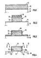
- FIG. 1 represents a surface portion of a semiconductor body 10, for example made of p-type silicon, which is surmounted by an insulating grid layer 11, preferably made of silicon oxide, with a thickness close to 20 nm.
- a first polycrystalline layer 12, of a thickness of approximately 300 nm was then deposited on the insulating gate layer 11.
- the first polycrystalline layer 12 was made conductive by doping at a high concentration according to one of the usual technique in particular by doping during the deposit.
- first insulating layer 13 made of silicon oxide, with a thickness of 60 nm for example, which is intended to serve later as a stripping stop.
- a localized stripping of the first insulating layer 13 and of the first polycrystalline layer 12 is then carried out so as to form grid islands 15 according to known anisotropic etching techniques and using a photosensitive resin mask 16.
- the grid islands 15 can be obtained by first carrying out a selective and localized etching of the first insulating layer 13 in a plasma containing a mixture of fluorine and oxygen ions, then by removing the mask of photosensitive resin 16 using an oxygen plasma, then finally, by selectively pickling the first polycrystalline layer 12 in the windows previously opened in the first insulating layer 13, using a plasma containing mainly chlorine ions.
- the pickling of the polycrystalline material being selective with respect to silicon oxide, the gate oxide layer 11, although relatively thin, constitutes a pickling stop at the end of the operation. .
- a protective layer of an anti-oxidation material 20 such as silicon nitride with a thickness of between 15 and 50 nm and preferably close to 30 nm is deposited by a method which ensures the most uniform possible coverage of the contours of the surface of the device including the substantially vertical portions of the edges of the grid islands 15.
- LPCVD chemical vapor deposition under reduced pressure
- the bulk of the protective layer 20 is then stripped of silicon nitride by an anisotropic pickling method, for example pickling with reactive fluorine or chlorine ions so as to form narrow temporary spacers 20a for protecting the edges of the islets.
- grid 15 as shown in Figure 4.
- the pickling of silicon nitride is not always selective with regard to the pickling of silicon oxide.
- the parts of the unprotected grid insulating layer 11 which are located outside the grid islands 15 are eliminated because this insulating layer is thin.
- at least a substantial portion of the first insulating layer 13 can be maintained on the upper surface of the grid island 15 because of its comparatively large thickness.
- the next step is the ion implantation of an n-type doping element, symbolized by the arrows 21, so as to form lightly doped portions of the source and drain regions 22, 23 using the grid islands 15 provided with the temporary spacers 20a as an implantation mask.
- this operation can be carried out by implantation of phosphorus at a dose of 4.1013 at / cm2, with an energy of 50 to 60 keV.
- the first insulating layer 13 is then reformed - respectively regenerated - according to whether it was completely eliminated previously or kept over a portion of its thickness.
- a layer of silicon oxide 24 with a thickness of the order of 10 to 15 nm is formed, while the portions of insulating gate layer 11 located under the temporary spacers 20a and whose integrity has a decisive influence on the operation of the device are regenerated by a lateral oxidation effect under the spacers provisional 20a.
- the temporary spacers 20a are first removed by selective pickling, for example by the wet route, in hot phosphoric acid (140 ° C.).
- a second polycrystalline layer 30 is then deposited with a thickness of approximately 50 nm, made conductive by doping. This operation is preferably carried out by a method ensuring good coverage of the edges of the grid islands 15 and for example by chemical vapor deposition under reduced pressure.
- the second polycrystalline layer 30 is isolated above the grid islands 15 by the first insulating layer 13, it is on the contrary in electrical contact with the first polycrystalline layer 12 on the edges 15a of the islands of grid 15, edges which have been protected during the reoxidation step by the temporary spacers 20a made of silicon nitride.
- an ion implantation symbolized by the arrows 31 with a view to producing additional portions 22a and 23a of the source and drain regions, with intermediate doping (n+) making it possible to ensure a more progressive variation of the doping in a lateral direction between the channel and the drain and source regions with high doping.
- Such an ion implantation operation can be carried out for example with phosphorus, at a dose of 2.1014 at / cm2 at an energy of 50 to 70 keV.
- insulating spacers 32 are then produced on the edges of the grid islands 15 according to a technique known per se, which essentially consists in depositing a second relatively thick insulating layer of the order of 200 nm, made of silicon oxide, then to remove most of this layer by anisotropic pickling, the second polycrystalline layer 30 forming pickling stop for this operation.
- FIG. 8 consists in removing most of the second polycrystalline layer 30, that is to say say the portions which are not protected by silicon oxide (first insulating layer 13 and insulating spacers 32) so as to form enlarged grid islands 35, from grid islands 15, the dimensions of which are increased by the width of the insulating spacers 32.
- source implantation and drain regions are produced by ion implantation represented by the arrows 36, heavily doped portions (n termee) 22b, 23b respectively. This can be done with Arsenic ions, at a dose of 2.1015 At / cm2 and with an energy of 100 keV.
- the remaining portions of the second L-shaped polycrystalline layer 30 which are in electrical contact with the portion of the first polycrystalline layer 12 of the grid island 15 produce with the first polycrystalline layer an inverted T-shaped gate electrode which covers the lightly doped portions 22, 23 of the source and drain regions as well as any intermediate doped portions 22a, 23a.
- This gate electrode extends laterally towards the heavily doped portions 22b, 23b of the source and drain regions.
- source and drain regions with different doping, 22, 23, 22a, 23a, 22b, 23b are arranged in a laterally stepped manner in the order which is suitable for promoting a high breakdown voltage of the diode. drain / substrate and to reduce the emission of high energy charge carriers at the passage of this junction.
- the device can be finished by opening localized contact windows by means of a photosensitive mask according to usual well-known techniques which it is not useful to describe in more detail here.
- Figures 9 and 10 show another embodiment of the invention, making it possible to form metallic contact areas on the device by a self-alignment technique.
- the removal by selective pickling of the second polycrystalline layer 30 which is not protected by the insulating spacers 32 is extended for a determined period under isotropic pickling conditions so as to form grooves 40 on either side of the grid islands 15 as well as grooves 41 under the insulating spacers 32 between these and the insulating layer 24.
- These grooves are produced in the second polycrystalline layer 30 by lateral pickling in the unprotected parts of this layer.
- a layer of insulating material having selective pickling properties is deposited over the entire device, for example a layer of silicon nitride 42 with a thickness of approximately 100 nm by a method ensuring good surface coverage by example the chemical vapor deposition method under reduced pressure, so as to at least fill the grooves 40 and 41 with silicon nitride.
- the layer of silicon nitride 40 is then pickled anisotropically so as to keep only this portion 42a and 42b of this layer, filling the grooves 40 and 41 respectively.
- the whole device is then subjected to a pickling of the silicon oxide present on the surface, selectively with respect to the silicon nitride, as well as with respect to the polycrystalline and monocrystalline silicon.
- the first insulating layer 13 is completely removed so as to expose the first polycrystalline layer 2 of the gate island as well as the contact zones 47 and 48 of the source and drain regions.
- the outline of the first insulating layer 13 as well as of the insulating spacers 32 before this operation is indicated respectively by the dotted lines 45 and 46. Given their large thickness, the major part of the insulating spacers 32 is retained after this operation.
- a MIS type transistor device is again obtained having an inverted T-shaped gate electrode which covers the lightly doped portions 22 and 23 of the source and drain regions and which extends through the remaining portions of the second polycrystalline layer 30, L-shaped, towards the heavily doped portions 22b and 23b of the source and drain regions.
- the lateral extension of this gate electrode is controlled during the etching step of the second polycrystalline layer 30.
- FIGS. 9 and 10 there have been shown no intermediate doped portions of the source and drain regions such that those described in FIG. 8 in the first embodiment of the invention, but of course these additional intermediate doped portions can also be produced in the embodiment which has just been described.
- contact with the grid island 15 is made at another location, away from the section plane of the figures.
- first insulating layer 13 is deposited in two stages: a first stage of depositing a very thick layer, for example 250 nm of silicon oxide, which is kept only at the locations to be protected, by localized pickling, then a second step of depositing a layer of silicon oxide 60nm thick, covering the entire device.
Landscapes
- Insulated Gate Type Field-Effect Transistor (AREA)
- Metal-Oxide And Bipolar Metal-Oxide Semiconductor Integrated Circuits (AREA)
Applications Claiming Priority (2)
| Application Number | Priority Date | Filing Date | Title |
|---|---|---|---|
| FR8914435A FR2654258A1 (fr) | 1989-11-03 | 1989-11-03 | Procede pour fabriquer un dispositif a transistor mis ayant une electrode de grille en forme de "t" inverse. |
| FR8914435 | 1989-11-03 |
Publications (1)
| Publication Number | Publication Date |
|---|---|
| EP0426251A1 true EP0426251A1 (de) | 1991-05-08 |
Family
ID=9387060
Family Applications (1)
| Application Number | Title | Priority Date | Filing Date |
|---|---|---|---|
| EP90202860A Withdrawn EP0426251A1 (de) | 1989-11-03 | 1990-10-29 | Verfahren zur Herstellung eines MIS-Transistor-Bauelementes mit einer invertierten T-förmigen Gitterelektrode |
Country Status (4)
| Country | Link |
|---|---|
| US (1) | US5015598A (de) |
| EP (1) | EP0426251A1 (de) |
| JP (1) | JPH03157938A (de) |
| FR (1) | FR2654258A1 (de) |
Cited By (2)
| Publication number | Priority date | Publication date | Assignee | Title |
|---|---|---|---|---|
| FR2676864A1 (fr) * | 1991-05-23 | 1992-11-27 | Samsung Electronics Co Ltd | Procede de fabrication de transistor mos a recouvrement grille-drain et structure correspondante. |
| EP0547907A3 (de) * | 1991-12-18 | 1993-08-04 | STMicroelectronics, Inc. | Verfahren zur Bildung einer Torelektrode, welche eine LDD-Struktur überlappt |
Families Citing this family (59)
| Publication number | Priority date | Publication date | Assignee | Title |
|---|---|---|---|---|
| US5153145A (en) * | 1989-10-17 | 1992-10-06 | At&T Bell Laboratories | Fet with gate spacer |
| FR2663157B1 (fr) * | 1990-06-12 | 1992-08-07 | Thomson Csf | Procede d'autoalignement des contacts metalliques sur un dispositif semiconducteur et semiconducteur autoaligne. |
| US5306655A (en) * | 1990-07-24 | 1994-04-26 | Matsushita Electric Industrial Co., Ltd. | Structure and method of manufacture for MOS field effect transistor having lightly doped drain and source diffusion regions |
| US5061647A (en) * | 1990-10-12 | 1991-10-29 | Motorola, Inc. | ITLDD transistor having variable work function and method for fabricating the same |
| KR100307272B1 (ko) * | 1990-12-04 | 2002-05-01 | 하라 레이노스케 | Mos소자제조방법 |
| US5102815A (en) * | 1990-12-19 | 1992-04-07 | Intel Corporation | Method of fabricating a composite inverse T-gate metal oxide semiconductor device |
| EP0513415A1 (de) * | 1991-05-16 | 1992-11-19 | Kabushiki Kaisha Toshiba | FET mit isoliertem Gate mit doppel-schichtigen Wannen von niedriger und höherer Störstoffkonzentrationen und sein Herstellungsverfahren |
| US5244823A (en) * | 1991-05-21 | 1993-09-14 | Sharp Kabushiki Kaisha | Process for fabricating a semiconductor device |
| US5401994A (en) * | 1991-05-21 | 1995-03-28 | Sharp Kabushiki Kaisha | Semiconductor device with a non-uniformly doped channel |
| US5292670A (en) * | 1991-06-10 | 1994-03-08 | Texas Instruments Incorporated | Sidewall doping technique for SOI transistors |
| KR100274555B1 (ko) * | 1991-06-26 | 2000-12-15 | 윌리엄 비. 켐플러 | 절연 게이트 전계 효과 트랜지스터 구조물 및 이의 제조 방법 |
| WO1993009567A1 (en) * | 1991-10-31 | 1993-05-13 | Vlsi Technology, Inc. | Auxiliary gate lightly doped drain (agldd) structure with dielectric sidewalls |
| EP0789399B1 (de) * | 1993-01-12 | 2001-11-07 | Sony Corporation | Ausgangsschaltung für Ladungsübertragungselement |
| US5358879A (en) * | 1993-04-30 | 1994-10-25 | Loral Federal Systems Company | Method of making gate overlapped lightly doped drain for buried channel devices |
| US5308777A (en) * | 1993-07-28 | 1994-05-03 | United Microelectronics Corporation | Mask ROM process |
| KR100189964B1 (ko) * | 1994-05-16 | 1999-06-01 | 윤종용 | 고전압 트랜지스터 및 그 제조방법 |
| US5506161A (en) * | 1994-10-24 | 1996-04-09 | Motorola, Inc. | Method of manufacturing graded channels underneath the gate electrode extensions |
| US5783475A (en) * | 1995-11-13 | 1998-07-21 | Motorola, Inc. | Method of forming a spacer |
| US5686329A (en) * | 1995-12-29 | 1997-11-11 | Taiwan Semiconductor Manufacturing Company, Ltd. | Method for forming a metal oxide semiconductor field effect transistor (MOSFET) having improved hot carrier immunity |
| US5739066A (en) | 1996-09-17 | 1998-04-14 | Micron Technology, Inc. | Semiconductor processing methods of forming a conductive gate and line |
| US5909622A (en) * | 1996-10-01 | 1999-06-01 | Advanced Micro Devices, Inc. | Asymmetrical p-channel transistor formed by nitrided oxide and large tilt angle LDD implant |
| US5985724A (en) * | 1996-10-01 | 1999-11-16 | Advanced Micro Devices, Inc. | Method for forming asymmetrical p-channel transistor having nitrided oxide patterned to selectively form a sidewall spacer |
| US5893739A (en) * | 1996-10-01 | 1999-04-13 | Advanced Micro Devices, Inc. | Asymmetrical P-channel transistor having a boron migration barrier and a selectively formed sidewall spacer |
| KR100205320B1 (ko) * | 1996-10-25 | 1999-07-01 | 구본준 | 모스펫 및 그 제조방법 |
| US5869879A (en) * | 1996-12-06 | 1999-02-09 | Advanced Micro Devices, Inc. | CMOS integrated circuit having a sacrificial metal spacer for producing graded NMOS source/drain junctions dissimilar from PMOS source/drain junctions |
| US5766969A (en) * | 1996-12-06 | 1998-06-16 | Advanced Micro Devices, Inc. | Multiple spacer formation/removal technique for forming a graded junction |
| US5869866A (en) | 1996-12-06 | 1999-02-09 | Advanced Micro Devices, Inc. | Integrated circuit having sacrificial spacers for producing graded NMOS source/drain junctions possibly dissimilar from PMOS source/drain junctions |
| KR100204805B1 (ko) * | 1996-12-28 | 1999-06-15 | 윤종용 | 디엠오에스 트랜지스터 제조방법 |
| US5895955A (en) * | 1997-01-10 | 1999-04-20 | Advanced Micro Devices, Inc. | MOS transistor employing a removable, dual layer etch stop to protect implant regions from sidewall spacer overetch |
| US5793089A (en) * | 1997-01-10 | 1998-08-11 | Advanced Micro Devices, Inc. | Graded MOS transistor junction formed by aligning a sequence of implants to a selectively removable polysilicon sidewall space and oxide thermally grown thereon |
| JPH10223889A (ja) * | 1997-02-04 | 1998-08-21 | Mitsubishi Electric Corp | Misトランジスタおよびその製造方法 |
| US20020137890A1 (en) * | 1997-03-31 | 2002-09-26 | Genentech, Inc. | Secreted and transmembrane polypeptides and nucleic acids encoding the same |
| US5963809A (en) * | 1997-06-26 | 1999-10-05 | Advanced Micro Devices, Inc. | Asymmetrical MOSFET with gate pattern after source/drain formation |
| TW339470B (en) * | 1997-09-01 | 1998-09-01 | United Microelectronics Corp | The manufacturing method for spacer |
| TW370719B (en) * | 1997-10-23 | 1999-09-21 | Winbond Electronics Corp | Manufacturing method of anti-electrostatic discharge element |
| US6063668A (en) * | 1997-12-18 | 2000-05-16 | Advanced Micro Devices, Inc. | Poly I spacer manufacturing process to eliminate polystringers in high density nand-type flash memory devices |
| US6281078B1 (en) | 1997-12-18 | 2001-08-28 | Advanced Micro Devices, Inc. | Manufacturing process to eliminate ONO fence material in high density NAND-type flash memory devices |
| US5994239A (en) * | 1997-12-18 | 1999-11-30 | Advanced Micro Devices, Inc. | Manufacturing process to eliminate polystringers in high density nand-type flash memory devices |
| US5837588A (en) * | 1998-01-26 | 1998-11-17 | Texas Instruments-Acer Incorporated | Method for forming a semiconductor device with an inverse-T gate lightly-doped drain structure |
| US6472281B2 (en) * | 1998-02-03 | 2002-10-29 | Matsushita Electronics Corporation | Method for fabricating semiconductor device using a CVD insulator film |
| JP2000012864A (ja) * | 1998-06-22 | 2000-01-14 | Semiconductor Energy Lab Co Ltd | 半導体装置の作製方法 |
| US6124610A (en) | 1998-06-26 | 2000-09-26 | Advanced Micro Devices, Inc. | Isotropically etching sidewall spacers to be used for both an NMOS source/drain implant and a PMOS LDD implant |
| US6143611A (en) * | 1998-07-30 | 2000-11-07 | Micron Technology, Inc. | Semiconductor processing methods, methods of forming electronic components, and transistors |
| JP4476390B2 (ja) * | 1998-09-04 | 2010-06-09 | 株式会社半導体エネルギー研究所 | 半導体装置の作製方法 |
| US6245626B1 (en) * | 1999-07-07 | 2001-06-12 | United Microelectronics Corp. | Method of fabricating a MOS device using a sacrificial layer and spacer |
| US6274446B1 (en) | 1999-09-28 | 2001-08-14 | International Business Machines Corporation | Method for fabricating abrupt source/drain extensions with controllable gate electrode overlap |
| US6492275B2 (en) | 2000-01-21 | 2002-12-10 | Advanced Micro Devices, Inc. | Control of transistor performance through adjustment of spacer oxide profile with a wet etch |
| FR2815174A1 (fr) * | 2000-10-06 | 2002-04-12 | St Microelectronics Sa | Transistors mos miniaturises de type ldd |
| KR100414220B1 (ko) * | 2001-06-22 | 2004-01-07 | 삼성전자주식회사 | 공유 콘택을 가지는 반도체 장치 및 그 제조 방법 |
| KR100395878B1 (ko) * | 2001-08-31 | 2003-08-25 | 삼성전자주식회사 | 스페이서 형성 방법 |
| US6911695B2 (en) * | 2002-09-19 | 2005-06-28 | Intel Corporation | Transistor having insulating spacers on gate sidewalls to reduce overlap between the gate and doped extension regions of the source and drain |
| JPWO2004112139A1 (ja) * | 2003-06-10 | 2006-09-28 | 富士通株式会社 | 半導体装置とその製造方法 |
| US6913980B2 (en) * | 2003-06-30 | 2005-07-05 | Texas Instruments Incorporated | Process method of source drain spacer engineering to improve transistor capacitance |
| JP2007508705A (ja) * | 2003-10-17 | 2007-04-05 | コーニンクレッカ フィリップス エレクトロニクス エヌ ヴィ | 半導体装置とこの種の半導体装置の製造方法 |
| US7135372B2 (en) * | 2004-09-09 | 2006-11-14 | Taiwan Semiconductor Manufacturing Company, Ltd. | Strained silicon device manufacturing method |
| US7642152B2 (en) * | 2005-09-07 | 2010-01-05 | United Microelectronics Corp. | Method of fabricating spacers and cleaning method of post-etching and semiconductor device |
| US8878177B2 (en) * | 2011-11-11 | 2014-11-04 | Semiconductor Energy Laboratory Co., Ltd. | Semiconductor device and method for manufacturing semiconductor device |
| JP6063117B2 (ja) * | 2011-11-11 | 2017-01-18 | 株式会社半導体エネルギー研究所 | 半導体装置 |
| US9941388B2 (en) * | 2014-06-19 | 2018-04-10 | Globalfoundries Inc. | Method and structure for protecting gates during epitaxial growth |
Citations (3)
| Publication number | Priority date | Publication date | Assignee | Title |
|---|---|---|---|---|
| DE3530065A1 (de) * | 1984-08-22 | 1986-03-06 | Mitsubishi Denki K.K., Tokio/Tokyo | Verfahren zur herstellung eines halbleiters |
| EP0173953A2 (de) * | 1984-08-28 | 1986-03-12 | Kabushiki Kaisha Toshiba | Verfahren zum Herstellen einer Halbleiteranordnung mit Gateelektrode |
| US4868617A (en) * | 1988-04-25 | 1989-09-19 | Elite Semiconductor & Sytems International, Inc. | Gate controllable lightly doped drain mosfet devices |
Family Cites Families (16)
| Publication number | Priority date | Publication date | Assignee | Title |
|---|---|---|---|---|
| JPS54161282A (en) * | 1978-06-12 | 1979-12-20 | Toshiba Corp | Manufacture of mos semiconductor device |
| JPS5764973A (en) * | 1980-10-09 | 1982-04-20 | Nec Corp | Manufacture os semiconductor device |
| JPS58200576A (ja) * | 1982-05-18 | 1983-11-22 | Oki Electric Ind Co Ltd | Mos型電界効果トランジスタの製造方法 |
| JPS6055665A (ja) * | 1983-09-06 | 1985-03-30 | Toshiba Corp | 半導体装置の製造方法 |
| JPH067556B2 (ja) * | 1985-03-15 | 1994-01-26 | 株式会社東芝 | Mis型半導体装置 |
| JPH0834310B2 (ja) * | 1987-03-26 | 1996-03-29 | 沖電気工業株式会社 | 半導体装置の製造方法 |
| JPH0666326B2 (ja) * | 1987-03-17 | 1994-08-24 | 松下電器産業株式会社 | 半導体装置およびその製造方法 |
| KR970003903B1 (en) * | 1987-04-24 | 1997-03-22 | Hitachi Mfg Kk | Semiconductor device and fabricating method thereof |
| US4837180A (en) * | 1987-07-09 | 1989-06-06 | Industrial Technology Research Institute | Ladder gate LDDFET |
| US4818715A (en) * | 1987-07-09 | 1989-04-04 | Industrial Technology Research Institute | Method of fabricating a LDDFET with self-aligned silicide |
| JP2568412B2 (ja) * | 1987-07-29 | 1997-01-08 | 日成ビルド工業株式会社 | 地下駐車場用のスタッカクレーン |
| US4963504A (en) * | 1987-11-23 | 1990-10-16 | Xerox Corporation | Method for fabricating double implanted LDD transistor self-aligned with gate |
| US4907048A (en) * | 1987-11-23 | 1990-03-06 | Xerox Corporation | Double implanted LDD transistor self-aligned with gate |
| JPH0666329B2 (ja) * | 1988-06-30 | 1994-08-24 | 株式会社東芝 | 半導体装置の製造方法 |
| US4906589A (en) * | 1989-02-06 | 1990-03-06 | Industrial Technology Research Institute | Inverse-T LDDFET with self-aligned silicide |
| US4951100A (en) * | 1989-07-03 | 1990-08-21 | Motorola, Inc. | Hot electron collector for a LDD transistor |
-
1989
- 1989-11-03 FR FR8914435A patent/FR2654258A1/fr active Pending
-
1990
- 1990-09-25 US US07/588,116 patent/US5015598A/en not_active Expired - Fee Related
- 1990-10-29 EP EP90202860A patent/EP0426251A1/de not_active Withdrawn
- 1990-11-01 JP JP2297028A patent/JPH03157938A/ja active Pending
Patent Citations (3)
| Publication number | Priority date | Publication date | Assignee | Title |
|---|---|---|---|---|
| DE3530065A1 (de) * | 1984-08-22 | 1986-03-06 | Mitsubishi Denki K.K., Tokio/Tokyo | Verfahren zur herstellung eines halbleiters |
| EP0173953A2 (de) * | 1984-08-28 | 1986-03-12 | Kabushiki Kaisha Toshiba | Verfahren zum Herstellen einer Halbleiteranordnung mit Gateelektrode |
| US4868617A (en) * | 1988-04-25 | 1989-09-19 | Elite Semiconductor & Sytems International, Inc. | Gate controllable lightly doped drain mosfet devices |
Non-Patent Citations (1)
| Title |
|---|
| IEEE TRANSACTIONS ON ELECTRON DEVICES, vol. 35, no. 12, décembre 1988, pages 2088-2093, IEEE, New York, US; R. IZAWA et al.: "Impact of the gate-drain overlapped device (GOLD) for deep submicrometer VLSI" * |
Cited By (2)
| Publication number | Priority date | Publication date | Assignee | Title |
|---|---|---|---|---|
| FR2676864A1 (fr) * | 1991-05-23 | 1992-11-27 | Samsung Electronics Co Ltd | Procede de fabrication de transistor mos a recouvrement grille-drain et structure correspondante. |
| EP0547907A3 (de) * | 1991-12-18 | 1993-08-04 | STMicroelectronics, Inc. | Verfahren zur Bildung einer Torelektrode, welche eine LDD-Struktur überlappt |
Also Published As
| Publication number | Publication date |
|---|---|
| FR2654258A1 (fr) | 1991-05-10 |
| US5015598A (en) | 1991-05-14 |
| JPH03157938A (ja) | 1991-07-05 |
Similar Documents
| Publication | Publication Date | Title |
|---|---|---|
| EP0426250B1 (de) | Verfahren zur Herstellung eines MIS-Transistor-Bauelementes mit einem Gitter, welches über geringdotierte Teile der Source- und Drain-Gebiete herausragt | |
| FR2654258A1 (fr) | Procede pour fabriquer un dispositif a transistor mis ayant une electrode de grille en forme de "t" inverse. | |
| EP1266409B1 (de) | Mos-transistor mit metallischen source- und draingebieten und dessen herstellungsverfahren | |
| EP1145300B1 (de) | Verfahren zur herstellung eines mis-transistors auf einem halbleitersubstrat | |
| EP2323160A1 (de) | Verfahren zur Herstellung von Feldeffekttransistoren mit einer Gegenelektrode und Halbleitervorrichtung | |
| FR2823009A1 (fr) | Procede de fabrication d'un transistor vertical a grille isolee a faible recouvrement de la grille sur la source et sur le drain, et circuit integre comportant un tel transistor | |
| EP0420748A1 (de) | Verfahren zur Herstellung einer Hochspannungs-MIS-integrierten Schaltung | |
| FR2823010A1 (fr) | Procede de fabrication d'un transistor vertical a grille isolee a quadruple canal de conduction, et circuit integre comportant un tel transistor | |
| EP2009682A1 (de) | Vom Substrat isolierter Finfet-Feldeffekttransistor | |
| FR3043837A1 (fr) | Procede de realisation de transistor a nanofil semi-conducteur et comprenant une grille et des espaceurs auto-alignes | |
| EP1192653A1 (de) | Seitenätzungverfahren mittels löchern zur herstellung von halbleiterbauelementen | |
| FR2676864A1 (fr) | Procede de fabrication de transistor mos a recouvrement grille-drain et structure correspondante. | |
| EP1346405B1 (de) | Verfahren zur herstellung einer zwischen elektroden eingefügten inselstruktur und deren anwendung auf transistoren | |
| EP1218942A1 (de) | Halbleiterbauelement mit den vorteilen von den soi und massiv aufbau und verfahren zur deren herstellung | |
| EP0190243B1 (de) | Verfahren zur herstellung einer integrierten schaltung vom mis-typ | |
| EP0209419B1 (de) | Verfahren zur Herstellung von mindestens zwei mit einer dielektrischen Schicht versehenen Metallisierungen auf einem Halbleiterkörper und Halbleiteranordnung mit dieser Schicht | |
| EP0522938B1 (de) | Verfahren zum Herstellen eines vertikalen Feldeffekt-Transistors und durch dieses Verfahren hergestellter Transistor | |
| EP4386634A1 (de) | Austauschelektroden für quanteninselgitter | |
| FR2791178A1 (fr) | NOUVEAU DISPOSITIF SEMI-CONDUCTEUR COMBINANT LES AVANTAGES DES ARCHITECTURES MASSIVE ET soi, ET PROCEDE DE FABRICATION | |
| FR2848726A1 (fr) | Transistor mis a grille auto-alignee et son procede de fabrication | |
| EP1328969B1 (de) | Herstellungsverfahren eines mos-transistors | |
| EP0197838A1 (de) | Verfahren zum Herstellen eines Feldeffekttransistors mit selbstausrichtender Gate-Metallisierung | |
| FR2976401A1 (fr) | Composant electronique comportant un ensemble de transistors mosfet et procede de fabrication | |
| EP4006996A2 (de) | Quantenvorrichtung und ihr herstellungsverfahren | |
| FR2679379A1 (fr) | Procede de fabrication de circuits integres avec electrodes tres etroites. |
Legal Events
| Date | Code | Title | Description |
|---|---|---|---|
| PUAI | Public reference made under article 153(3) epc to a published international application that has entered the european phase |
Free format text: ORIGINAL CODE: 0009012 |
|
| AK | Designated contracting states |
Kind code of ref document: A1 Designated state(s): DE FR GB IT NL |
|
| STAA | Information on the status of an ep patent application or granted ep patent |
Free format text: STATUS: THE APPLICATION IS DEEMED TO BE WITHDRAWN |
|
| 18D | Application deemed to be withdrawn |
Effective date: 19911108 |