EP0422806A2 - Magnetoresistiver Wandler - Google Patents
Magnetoresistiver Wandler Download PDFInfo
- Publication number
- EP0422806A2 EP0422806A2 EP90310687A EP90310687A EP0422806A2 EP 0422806 A2 EP0422806 A2 EP 0422806A2 EP 90310687 A EP90310687 A EP 90310687A EP 90310687 A EP90310687 A EP 90310687A EP 0422806 A2 EP0422806 A2 EP 0422806A2
- Authority
- EP
- European Patent Office
- Prior art keywords
- magnetoresistive
- transducer
- layer
- read transducer
- active region
- Prior art date
- Legal status (The legal status is an assumption and is not a legal conclusion. Google has not performed a legal analysis and makes no representation as to the accuracy of the status listed.)
- Granted
Links
Images

Classifications
-
- G—PHYSICS
- G11—INFORMATION STORAGE
- G11B—INFORMATION STORAGE BASED ON RELATIVE MOVEMENT BETWEEN RECORD CARRIER AND TRANSDUCER
- G11B5/00—Recording by magnetisation or demagnetisation of a record carrier; Reproducing by magnetic means; Record carriers therefor
- G11B5/127—Structure or manufacture of heads, e.g. inductive
- G11B5/33—Structure or manufacture of flux-sensitive heads, i.e. for reproduction only; Combination of such heads with means for recording or erasing only
- G11B5/39—Structure or manufacture of flux-sensitive heads, i.e. for reproduction only; Combination of such heads with means for recording or erasing only using magneto-resistive devices or effects
- G11B5/3903—Structure or manufacture of flux-sensitive heads, i.e. for reproduction only; Combination of such heads with means for recording or erasing only using magneto-resistive devices or effects using magnetic thin film layers or their effects, the films being part of integrated structures
Definitions
- This invention relates to thin film magnetic heads and, more particularly to a magnetic head having a magnetoresistive read transducer.
- U.S. patent 3,840,898 discloses an MR sensor in which a transverse bias is produced.
- a magnetoresistive strip such as NiFe is treated in edge regions to produce a hard magnetic state.
- edge regions are arranged parallel to the direction of sense current and run along the entire strip to produce a transverse bias and would not produce longitudinal bias.
- the invention provides a magnetoresistive read transducer comprising: a magnetoresitive sensor having passive end regions separated by a central active region; a thin film of magnetoresistive conductive layer extending over substantially only said central active region; and a first and a second thin film of of hard magnetic material, each of said thin films of hard magnetic material forming an abutting junction having electrical and magnetic continuity with a respective different end of said magnetoresistive sensor.
- the invention also provides a method for making a magnetoresistive read transducer having passive end regions separated by a central active region comprising the steps of: depositing a thin magnetoresistive layer of ferromagnetic material over at least the central active region of said transducer; producing a stencil covering the central active region of said transducer; etching away the part of said magnetoresistive material not covered by said stencil to form the central active region of said transducer; depositing a film of hard magnetic material over regions of said transducer not covered by said stencil to produce the passive end regions of said transducer, said hard magnetic material in said end regions forming an abutting junction with a respective different end of said layer of magnetoresistive material so that a longitudinal bias is produced in each of said passive end regions of said transducer.
- the invention provides a magnetoresistive (MR) read transducer in which the MR layer extends over substantially only the central active region and a hard magnetic bias layer is provided in each end region which forms an abutting junction with the MR layer to produce a longitudinal bias in the MR sensor.
- MR magnetoresistive
- the MR read transducer comprises an MR sensor having passive end regions separated by a central active region.
- a thin MR layer of ferromagnetic is formed which extends over substantially only the central active region.
- a first and second film of hard magnetic material is formed extending over substantially only one of the passive end regions and forming an abutting junction having electrical and magnetic continuity with one end of the MR layer to produce a longitudinal bias in the MR sensor.
- the preferred method for making the MR read transducer comprises the steps of depositing a thin MR layer of ferromagnetic material over at least the central active region of the transducer, producing a stencil covering the central active region of the transducer, and etching away the part of the MR material not covered by the stencil. A film of hard magnetic material is then deposited over regions of the transducer not covered by the stencil to produce the passive end regions of the transducer with the hard magnetic material forming an abutting junction with one end of the MR material so that a longitudinal bias is produced in each of the passive end regions of the transducer.
- the preferred use of such magnetoresitive read transducers is in magnetic data storage devices such as hard discs.
- a prior art MR read transducer of the type described and claimed in U.S. patent 4,663,685 comprises an MR layer 11 which extends over the entire transducer 10′.
- An exchange bias layer 12 extends over the end regions 14 only to produce a longitudinal bias field and a soft magnetic film layer 15, separated from the MR layer 11 by a thin non-magnetic spacer layer 13, produces a transverse bias field in at least part of the central active region 16.
- the read signal is sensed over the central active region 16 which is defined in this embodiment by the spacing between conductors 18 and 20.
- the MR read transducer comprises an MR layer 22 which extends over substantially only the central active region 24 and a hard magnetic bias layer 26 in each end region 28 which forms an abutting junction 30 with the MR layer 22 to produce longitudinal bias in the MR read transducer 10.
- This embodiment does not require additional side-reading suppression components. Instead, the hard magnetic bias layer 26 in each end region 28 need only provide for electrical and magnetic continuity to the MR layer 22.
- the hard magnetic bias layer 26 can be provided with a single layer of metal such as Co Cr, Co Pt or Co Cr Pt, for example, although the use of under-and/or overcoats such as W or Au may be desirable.
- transverse bias is also required in the central active region 24, and this bias can be provided by soft film bias, shunt bias, barber pole bias configuration, or any other compatible transverse bias techniques.
- the transverse bias structure has not been shown in the conceptual view of Fig. 2.
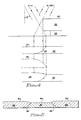
- FIGs. 3 a - d A specific embodiment of a process for fabricating a suitable junction between the MR layer 22 and the hard magnetic bias layer 26 is shown in Figs. 3 a - d.
- the process comprises the steps of depositing, upon a suitable substrate 21 a film of MR material such as NiFe, for example, over the length of the sensor.
- a transverse bias structure comprising a soft magnetic film 23 and non-magnetic spacer layer 25 are deposited on substrate 21 prior to deposition of the MR layer 22.
- the process then continues by depositing a film of a suitable material such as photoresist, and patterning the photoresist material to form a stencil 32 (Fig. 3a).
- Stencil 32 is used to define each edge of the MR layer 22 as the film of MR material 22 as well as the spacer layer 25 and the soft magnetic film 23 are subjected to a subtractive process such as sputter etching, ion milling or chemical etching to produce an MR trilayer structure 27 (Fig. 3b).
- the material for the hard magnetic bias layers 26 is then deposited as stencil 32 again defines edges of the bias layers 26 (Fig. 3c).
- a conductor layer is deposited to produce conductor leads 29 and 31. If desired, conductor leads 29 and 31 can be deposited in a later step if the conductor leads 29 and 31 are not coextensive with the hard bias layer 26.
- the preferred embodiment comprises a junction in which the topography is well controllable so that the junction can be produced easily and reliably.
- Fig. 4 shows in greater detail the formation of the contiguous junction according to an embodiment of the present invention.
- the stencil 32 comprises a bi-layer resist formed by a thin underlayer 33 and a thick imaging layer 34.
- One exposure and one develop step defines the edge profile of the resist.
- An undercut is created by dissolution of the underlayer 33 in a suitable developer with the undercut distance determined by the develop time.
- the unmasked areas of the layer of MR material 35 are then removed by the use of a unidirectional process such as ion milling, for example.
- the angle of incidence ⁇ is controlled by suitably tilting the substrate relative to the incident beam.
- circular symmetry is obtained by rotating the substrate about a normal to the substrate so that any given point sees the incident beam rotate conically about the azimuth angle ⁇ except near the stencil 32 whose edge shadows the film 35 during some segment of substrate revolution.
- Fig. 4 for an azimuth angle of 0 degrees, there is exposure of the film 35 to point C and the exposure limit point moves progressively to the left (as shown in Figure 4) until at an azimuth angle of 180 degrees the exposure limit point is moved to point a.
- the combined milling for this embodiment produces a curved taper 36 as a result of the removal during the milling process of the part 37 of the film shown in dashed lines.
- the hard magnetic bias layer 38 is then deposited, by sputtering, for example, during a similar orientation and rotation of the substrate to produce a deposition profile such as that shown in dashed lines 39.
- the combined junction profile resulting from the deposition of bias layer 38 is shown in full line.
- the layer of MR material 35 is shown as a single layer in Fig. 4, it will be recognized that the MR element may comprise other layers, such as transverse bias layers, for example.
- This junction profile comprises two overlapping tapers.
- the taper profile is determined by the height of the stencil 32, the selected angle of incidence ⁇ and the size of the undercut.
- the stencil thickness was about 1 ⁇ m and the angle of incidence ⁇ was in the range of 70 to 80 degrees.
- This selected combination produced a taper length of about five times the thickness of the sensor (ie. the magnetoresistive layer).
- the junction should be long, however, for magnetic reliability the junction should be short.
- junction lengths within the range of 3 to 5 times the sensor thickness were shown to be suitable.
- the magnetoresistive read transducer made by the above-described method is shown in Fig. 5 which shows the edge view of the sensor, i.e., the surface which is in close proximity to the magnetic recording medium from which previously recorded magnetic data is to be read.
- the transducer comprises an MR element 42 which extends over the central active region 44 of the transducer, and hard magnetic bias layers 46 which form an abutting junction 48 with the MR element 42.
- the hard magnetic bias layers 46 extend over the end regions 50 of the transducer so that a longitudinal bias can be produced in the end regions 50 only of the transducer.
Landscapes
- Engineering & Computer Science (AREA)
- Manufacturing & Machinery (AREA)
- Magnetic Heads (AREA)
Applications Claiming Priority (2)
| Application Number | Priority Date | Filing Date | Title |
|---|---|---|---|
| US419246 | 1989-10-10 | ||
| US07/419,246 US5018037A (en) | 1989-10-10 | 1989-10-10 | Magnetoresistive read transducer having hard magnetic bias |
Publications (3)
| Publication Number | Publication Date |
|---|---|
| EP0422806A2 true EP0422806A2 (de) | 1991-04-17 |
| EP0422806A3 EP0422806A3 (en) | 1993-03-03 |
| EP0422806B1 EP0422806B1 (de) | 1995-08-02 |
Family
ID=23661434
Family Applications (1)
| Application Number | Title | Priority Date | Filing Date |
|---|---|---|---|
| EP90310687A Expired - Lifetime EP0422806B1 (de) | 1989-10-10 | 1990-09-28 | Magnetoresistiver Wandler |
Country Status (4)
| Country | Link |
|---|---|
| US (1) | US5018037A (de) |
| EP (1) | EP0422806B1 (de) |
| JP (1) | JPH07122925B2 (de) |
| DE (1) | DE69021315T2 (de) |
Cited By (14)
| Publication number | Priority date | Publication date | Assignee | Title |
|---|---|---|---|---|
| EP0558237A3 (de) * | 1992-02-28 | 1993-10-13 | International Business Machines Corporation | Magnetoresistiver Lesewandler mit verbessertem Vorspannungs-Profil |
| US5485334A (en) * | 1992-11-12 | 1996-01-16 | Quantum Peripherals Colorado, Inc. | Magnetoresistive device and method having improved Barkhausen noise suppression |
| EP0634740A3 (de) * | 1993-07-13 | 1996-01-31 | Ibm | Magnetoresistiver Lesewandler. |
| EP0676747A3 (de) * | 1994-04-07 | 1996-05-01 | Read Rite Corp | Magnetoresistiver Wandler mit isolierender Oxydaustauschschicht. |
| US5532892A (en) * | 1995-06-05 | 1996-07-02 | Quantum Peripherals Colorado, Inc. | Soft adjacent layer biased magnetoresistive device incorporating a natural flux closure design utilizing coplanar permanent magnet thin film stabilization |
| EP0682338A3 (de) * | 1994-05-13 | 1996-07-24 | Read Rite Corp | Magnetoresistive Struktur mit aneinandergrenzendem Übergang mit harter Polarisationsentwurf und mit Leitungswiderstand. |
| EP0703572A3 (de) * | 1994-09-26 | 1996-07-31 | Read Rite Corp | Mehrschichtige harte Filme für longitudinale Vorspannung in magnetoresistiven Wandlern |
| EP0727773A1 (de) * | 1995-02-16 | 1996-08-21 | TDK Corporation | Magnetoresistiver Kopf |
| US5573809A (en) * | 1995-06-05 | 1996-11-12 | Quantum Peripherals Colorado, Inc. | Process for forming a magnetoresistive device |
| EP0747886A3 (de) * | 1995-06-05 | 1997-02-26 | Quantum Peripherals Colorado | Mit einer weichmagnetischen benachbarten Schicht vorgespannte magnetoresistive Anordnung, so aufgebaut, dass der Fluss sich natürlich schliesst, die mit einer koplanaren Permanent-Magnet-Dünnschicht stabilisiert wird, und Verfahren zu deren Herstellung |
| US5654854A (en) * | 1995-11-30 | 1997-08-05 | Quantum Corporation | Longitudinally biased magnetoresistive sensor having a concave shaped active region to reduce Barkhausen noise by achieving a substantially single magnetic domain state |
| US5664316A (en) * | 1995-01-17 | 1997-09-09 | International Business Machines Corporation | Method of manufacturing magnetoresistive read transducer having a contiguous longitudinal bias layer |
| US5708358A (en) * | 1996-03-21 | 1998-01-13 | Read-Rite Corporation | Spin valve magnetoresistive transducers having permanent magnets |
| CN1064163C (zh) * | 1994-04-21 | 2001-04-04 | 国际商业机器公司 | 双元件磁致电阻传感器 |
Families Citing this family (129)
| Publication number | Priority date | Publication date | Assignee | Title |
|---|---|---|---|---|
| JPH03242983A (ja) | 1990-02-06 | 1991-10-29 | Internatl Business Mach Corp <Ibm> | 磁気構造体の製造方法 |
| US5808843A (en) * | 1991-05-31 | 1998-09-15 | Hitachi, Ltd. | Magnetoresistance effect reproduction head |
| JPH0589435A (ja) * | 1991-09-27 | 1993-04-09 | Toshiba Corp | 磁気抵抗効果型磁気ヘツド |
| US5492605A (en) * | 1992-08-24 | 1996-02-20 | International Business Machines Corporation | Ion beam induced sputtered multilayered magnetic structures |
| SG47479A1 (en) * | 1992-08-25 | 1998-04-17 | Seagate Technology | A magnetoresistive sensor and method of making the same |
| US5669133A (en) * | 1992-08-25 | 1997-09-23 | Seagate Technology, Inc. | Method of making a magnetoresistive sensor |
| TW243530B (en) * | 1992-12-30 | 1995-03-21 | Ibm | Magnetoresistive sensor with improved microtrack profile for improved servo-positioning precision |
| EP0612061B1 (de) * | 1993-02-17 | 1998-08-26 | International Business Machines Corporation | Magnetoresistiver Lesewandler |
| US5966272A (en) * | 1993-06-21 | 1999-10-12 | Read-Rite Corporation | Magnetoresistive read head having an exchange layer |
| KR0131548B1 (ko) * | 1993-07-19 | 1998-04-18 | 윌리암 티. 엘리스 | 경사진 하드바이어스 자기저항성헤드를 갖는 자기저장시스템 |
| JP2683503B2 (ja) * | 1993-09-02 | 1997-12-03 | インターナショナル・ビジネス・マシーンズ・コーポレイション | 磁性膜構造 |
| US5479308A (en) * | 1993-11-15 | 1995-12-26 | Voegeli; Otto | Magnetoresistive transducer including interdiffusion layer |
| US5428491A (en) * | 1993-12-03 | 1995-06-27 | Eastman Kodak Company | Magnetoresistive head with deposited biasing magnet |
| WO1995026547A2 (en) * | 1994-03-25 | 1995-10-05 | Philips Electronics N.V. | Magneto-resistive device, and magnetic head comprising such a device |
| KR0153311B1 (ko) * | 1994-04-06 | 1998-12-15 | 가나이 쯔도무 | 자기 저항 효과형 박막 자기 헤드 및 그 제조 방법 |
| US5420736A (en) * | 1994-04-15 | 1995-05-30 | International Business Machines Corporation | MR read transducer with thermal noise cancellation |
| US6256222B1 (en) | 1994-05-02 | 2001-07-03 | Matsushita Electric Industrial Co., Ltd. | Magnetoresistance effect device, and magnetoresistaance effect type head, memory device, and amplifying device using the same |
| US5841611A (en) * | 1994-05-02 | 1998-11-24 | Matsushita Electric Industrial Co., Ltd. | Magnetoresistance effect device and magnetoresistance effect type head, memory device, and amplifying device using the same |
| JP3184400B2 (ja) * | 1994-06-07 | 2001-07-09 | アルプス電気株式会社 | 薄膜磁気ヘッドおよびその製造方法 |
| US5483402A (en) * | 1994-06-15 | 1996-01-09 | Quantum Corporation | Magneto resistive head having symmetric off-track performance profile |
| US5546254A (en) * | 1994-07-07 | 1996-08-13 | International Business Machines Corporation | Orthogonal MR Read head with single hard biased MR stripe |
| US5648031A (en) * | 1994-07-28 | 1997-07-15 | Custom Plastics Molding, Inc. | Method of forming antislip surfaces on thermoformed products |
| JPH0845029A (ja) * | 1994-08-01 | 1996-02-16 | Alps Electric Co Ltd | 薄膜磁気ヘッド |
| JPH0845030A (ja) * | 1994-08-03 | 1996-02-16 | Alps Electric Co Ltd | 磁気抵抗効果型磁気ヘッド |
| JP2694806B2 (ja) * | 1994-08-29 | 1997-12-24 | 日本電気株式会社 | 磁気抵抗効果素子およびその製造方法 |
| JPH0887721A (ja) * | 1994-09-16 | 1996-04-02 | Tdk Corp | 磁気変換素子及び薄膜磁気ヘッド |
| JP2720806B2 (ja) * | 1995-01-31 | 1998-03-04 | 日本電気株式会社 | 磁気抵抗効果型ヘッドおよびその製造方法 |
| US5646805A (en) * | 1995-03-06 | 1997-07-08 | Read-Rite Corporation | Magnetoresistive read transducer with partially abutted junctions |
| US5923503A (en) * | 1995-03-15 | 1999-07-13 | Alps Electric Co., Ltd. | Thin-film magnetic head and production method thereof |
| JP3448838B2 (ja) | 1995-06-30 | 2003-09-22 | 富士通株式会社 | 磁気抵抗効果型ヘッドの製造方法 |
| US5790351A (en) * | 1995-07-07 | 1998-08-04 | Nec Corporation | Magnetoresistive head with conductive underlayer |
| JP2849354B2 (ja) * | 1995-07-28 | 1999-01-20 | ティーディーケイ株式会社 | 磁気変換素子及び薄膜磁気ヘッド |
| US5754376A (en) * | 1995-09-12 | 1998-05-19 | Hitachi Metals, Ltd. | Magnetoresistive head with hard magnetic bias |
| US5935453A (en) * | 1995-11-16 | 1999-08-10 | International Business Machines Corporation | MR sensor having end regions with planar sides |
| US5793579A (en) * | 1995-11-30 | 1998-08-11 | Sanyo Electric Co., Ltd. | Thin film magnetic head and process for producing same |
| US5784772A (en) * | 1995-12-21 | 1998-07-28 | Storage Technology Corporation | Method of simultaneously forming MR sensors in a dual element MR head |
| KR100201681B1 (ko) * | 1996-01-03 | 1999-06-15 | 포만 제프리 엘 | 직교 자기저항 센서와 자기 저장 시스템 및 직교 자기저항 센서 제조 방법 |
| US6545847B2 (en) | 1996-02-14 | 2003-04-08 | Hitachi, Ltd. | Magnetoresistive effect head |
| US5936810A (en) | 1996-02-14 | 1999-08-10 | Hitachi, Ltd. | Magnetoresistive effect head |
| JPH09223304A (ja) * | 1996-02-15 | 1997-08-26 | Tdk Corp | 磁気ヘッド装置 |
| US5739987A (en) * | 1996-06-04 | 1998-04-14 | Read-Rite Corporation | Magnetoresistive read transducers with multiple longitudinal stabilization layers |
| US5930084A (en) | 1996-06-17 | 1999-07-27 | International Business Machines Corporation | Stabilized MR sensor and flux guide joined by contiguous junction |
| US5742459A (en) * | 1996-06-20 | 1998-04-21 | Read-Rite Corporation | Magnetic head having encapsulated magnetoresistive transducer and multilayered lead structure |
| US5742162A (en) * | 1996-07-17 | 1998-04-21 | Read-Rite Corporation | Magnetoresistive spin valve sensor with multilayered keeper |
| US5926348A (en) * | 1996-08-28 | 1999-07-20 | Yamaha Corporation | Magnetoresistive head having a magnetoresistive element with bent portions located at points of high longitudinal bias magnetic field intensity |
| US5739988A (en) * | 1996-09-18 | 1998-04-14 | International Business Machines Corporation | Spin valve sensor with enhanced magnetoresistance |
| SG72760A1 (en) * | 1996-09-19 | 2000-05-23 | Tdk Corp | Ferromagnetic tunnel junction magnetoresistive element and magnetic head |
| US7116527B1 (en) * | 1996-09-30 | 2006-10-03 | Kabushiki Kaisha Toshiba | Magnetoresistance effect device having hard magnetic film structural body |
| US5946169A (en) * | 1996-11-07 | 1999-08-31 | Seagate Technology, Inc. | Soft adjacent layer vertically biased magnetoresistive sensor having improved sensor stability |
| US5739990A (en) * | 1996-11-13 | 1998-04-14 | Read-Rite Corporation | Spin-valve GMR sensor with inbound exchange stabilization |
| JP3455037B2 (ja) * | 1996-11-22 | 2003-10-06 | アルプス電気株式会社 | スピンバルブ型薄膜素子、その製造方法、及びこのスピンバルブ型薄膜素子を用いた薄膜磁気ヘッド |
| US5729410A (en) * | 1996-11-27 | 1998-03-17 | International Business Machines Corporation | Magnetic tunnel junction device with longitudinal biasing |
| GB2336936B (en) | 1997-03-18 | 2001-01-10 | Seagate Technology | Improved magnetoresistive read sensor and method of fabricating a magnetoresistive read sensor |
| US5748416A (en) * | 1997-03-19 | 1998-05-05 | Hitachi Metals Ltd. | Magnetoresistive playback head |
| JP3253556B2 (ja) * | 1997-05-07 | 2002-02-04 | 株式会社東芝 | 磁気抵抗効果素子とそれを用いた磁気ヘッドおよび磁気記憶装置 |
| JP3699802B2 (ja) * | 1997-05-07 | 2005-09-28 | 株式会社東芝 | 磁気抵抗効果ヘッド |
| US6040962A (en) * | 1997-05-14 | 2000-03-21 | Tdk Corporation | Magnetoresistive element with conductive films and magnetic domain films overlapping a central active area |
| JP3263004B2 (ja) * | 1997-06-06 | 2002-03-04 | アルプス電気株式会社 | スピンバルブ型薄膜素子 |
| SG68063A1 (en) | 1997-07-18 | 1999-10-19 | Hitachi Ltd | Magnetoresistive effect type reproducing head and magnetic disk apparatus equipped with the reproducing head |
| US5982177A (en) * | 1997-08-08 | 1999-11-09 | Florida State University | Magnetoresistive sensor magnetically biased in a region spaced from a sensing region |
| JPH1196519A (ja) * | 1997-09-17 | 1999-04-09 | Alps Electric Co Ltd | スピンバルブ型薄膜素子およびその製造方法 |
| US6350487B1 (en) | 1997-09-24 | 2002-02-26 | Alps Electric Co., Ltd. | Spin-valve type thin film element and its manufacturing method |
| JPH11175920A (ja) | 1997-12-05 | 1999-07-02 | Nec Corp | 磁気抵抗効果型複合ヘッドおよびその製造方法 |
| JP3188232B2 (ja) * | 1997-12-09 | 2001-07-16 | アルプス電気株式会社 | 薄膜磁気ヘッドおよびその製造方法 |
| JP3269999B2 (ja) * | 1997-12-09 | 2002-04-02 | アルプス電気株式会社 | 薄膜磁気ヘッドの製造方法 |
| US5936293A (en) * | 1998-01-23 | 1999-08-10 | International Business Machines Corporation | Hard/soft magnetic tunnel junction device with stable hard ferromagnetic layer |
| US6356420B1 (en) | 1998-05-07 | 2002-03-12 | Seagate Technology Llc | Storage system having read head utilizing GMR and AMr effects |
| US6023395A (en) * | 1998-05-29 | 2000-02-08 | International Business Machines Corporation | Magnetic tunnel junction magnetoresistive sensor with in-stack biasing |
| US6005753A (en) * | 1998-05-29 | 1999-12-21 | International Business Machines Corporation | Magnetic tunnel junction magnetoresistive read head with longitudinal and transverse bias |
| JP2000011331A (ja) | 1998-06-18 | 2000-01-14 | Tdk Corp | 磁気抵抗効果素子及び薄膜磁気ヘッド |
| JP2000030223A (ja) | 1998-07-08 | 2000-01-28 | Tdk Corp | 磁気抵抗効果素子及び薄膜磁気ヘッド |
| US6097579A (en) * | 1998-08-21 | 2000-08-01 | International Business Machines Corporation | Tunnel junction head structure without current shunting |
| US6278594B1 (en) | 1998-10-13 | 2001-08-21 | Storage Technology Corporation | Dual element magnetoresistive read head with integral element stabilization |
| US6198609B1 (en) | 1998-11-09 | 2001-03-06 | Read-Rite Corporation | CPP Magnetoresistive device with reduced edge effect and method for making same |
| US6223420B1 (en) * | 1998-12-04 | 2001-05-01 | International Business Machines Corporation | Method of making a read head with high resistance soft magnetic flux guide layer for enhancing read sensor efficiency |
| JP3382866B2 (ja) * | 1998-12-18 | 2003-03-04 | 日本電気株式会社 | 磁気抵抗効果素子の製造方法 |
| US6587315B1 (en) | 1999-01-20 | 2003-07-01 | Alps Electric Co., Ltd. | Magnetoresistive-effect device with a magnetic coupling junction |
| JP3703348B2 (ja) | 1999-01-27 | 2005-10-05 | アルプス電気株式会社 | スピンバルブ型薄膜素子とそのスピンバルブ型薄膜素子を備えた薄膜磁気ヘッド |
| US6583971B1 (en) * | 1999-03-09 | 2003-06-24 | Sae Magnetics (Hk) Ltd. | Elimination of electric-pop noise in MR/GMR device |
| US6421212B1 (en) | 1999-09-21 | 2002-07-16 | Read-Rite Corporation | Thin film read head structure with improved bias magnet-to-magnetoresistive element interface and method of fabrication |
| US6139906A (en) * | 1999-10-07 | 2000-10-31 | Veeco Instruments, Inc. | Methods of depositing multilayer thin films |
| US6411476B1 (en) | 1999-10-28 | 2002-06-25 | International Business Machines Corporation | Trilayer seed layer structure for spin valve sensor |
| US6344953B1 (en) | 2000-03-08 | 2002-02-05 | Seagate Technology, Llc | Magnetoresistive read sensor using overlaid leads with insulating current guide layer |
| US6353318B1 (en) | 2000-03-10 | 2002-03-05 | Read-Rite Corporation | Magnetoresistive sensor having hard biased current perpendicular to the plane sensor |
| US6496334B1 (en) | 2000-05-26 | 2002-12-17 | Read-Rite Corportion | Data storage and retrieval apparatus with thin film read head having planarized extra gap and shield layers and method of fabrication thereof |
| GB2380052B (en) | 2000-07-13 | 2004-07-28 | Seagate Technology Llc | Domain control in shields of a magnetic transducer |
| US6504362B2 (en) * | 2000-07-13 | 2003-01-07 | Seagate Technology Llc | Process of measuring slide-reading of abutted-junction read heads |
| JP3260741B1 (ja) * | 2000-08-04 | 2002-02-25 | ティーディーケイ株式会社 | 磁気抵抗効果装置およびその製造方法ならびに薄膜磁気ヘッドおよびその製造方法 |
| US6801409B2 (en) | 2000-09-19 | 2004-10-05 | Seagate Technology Llc | Read head shield having improved stability |
| US6801408B1 (en) | 2000-11-02 | 2004-10-05 | Western Digital (Fremont), Inc. | Data storage and retrieval apparatus with thin film read head having a planar sensor element and an extra gap and method of fabrication thereof |
| US6577477B1 (en) | 2001-02-01 | 2003-06-10 | Headway Technologies, Inc. | Hard magnetic bias configuration for GMR |
| JP2003059014A (ja) | 2001-08-23 | 2003-02-28 | Hitachi Ltd | 磁気抵抗効果型ヘッド及びその製造方法 |
| US6636400B2 (en) | 2001-09-18 | 2003-10-21 | International Business Machines Corporation | Magnetoresistive head having improved hard biasing characteristics through the use of a multi-layered seed layer including an oxidized tantalum layer and a chromium layer |
| JP2003303406A (ja) | 2002-04-08 | 2003-10-24 | Hitachi Ltd | 磁気抵抗効果ヘッド及び磁気ヘッド |
| JP3828777B2 (ja) * | 2001-10-22 | 2006-10-04 | 株式会社日立グローバルストレージテクノロジーズ | 磁気抵抗効果ヘッド |
| US6861177B2 (en) * | 2002-02-21 | 2005-03-01 | Hitachi Global Storage Technologies Netherlands B.V. | Method of forming a read sensor using a lift-off mask having a hardmask layer and a release layer |
| US7139156B1 (en) | 2002-06-20 | 2006-11-21 | Storage Technology Corporation | Non-penetration of periodic structure to PM |
| US7007374B2 (en) * | 2002-08-09 | 2006-03-07 | Hitachi Global Storage Technologies Netherlands B.V. | Method of making a magnetic head |
| JP4284049B2 (ja) | 2002-09-25 | 2009-06-24 | 株式会社日立グローバルストレージテクノロジーズ | 磁気抵抗効果センサー及び磁気抵抗効果型ヘッド及びその製造方法 |
| US6985338B2 (en) * | 2002-10-21 | 2006-01-10 | International Business Machines Corporation | Insulative in-stack hard bias for GMR sensor stabilization |
| US7227726B1 (en) | 2002-11-12 | 2007-06-05 | Storage Technology Corporation | Method and system for providing a dual-stripe magnetoresistive element having periodic structure stabilization |
| JP4051271B2 (ja) | 2002-11-26 | 2008-02-20 | 株式会社日立グローバルストレージテクノロジーズ | 磁気記録ヘッド及び磁気記録再生装置 |
| US7555828B2 (en) * | 2002-12-02 | 2009-07-07 | Hitachi Global Storage Technologies Netherlands B.V. | Method for manufacturing a read sensor for a magnetoresistive head |
| JP2004193439A (ja) | 2002-12-13 | 2004-07-08 | Hitachi Ltd | 磁気抵抗効果ヘッド及びその製造方法 |
| JP2004272991A (ja) * | 2003-03-07 | 2004-09-30 | Hitachi Ltd | 磁気抵抗効果ヘッド |
| US20040209123A1 (en) * | 2003-04-17 | 2004-10-21 | Bajorek Christopher H. | Method of fabricating a discrete track recording disk using a bilayer resist for metal lift-off |
| US7099123B2 (en) * | 2003-07-29 | 2006-08-29 | Hitachi Global Storage Technologies | Self-pinned abutted junction heads having an arrangement of a second hard bias layer and a free layer for providing a net net longitudinal bias on the free layer |
| US7050277B2 (en) * | 2003-07-29 | 2006-05-23 | Hitachi Global Storage Technologies Netherlands B.V. | Apparatus having a self-pinned abutted junction magnetic read sensor with hard bias layers formed over ends of a self-pinned layer and extending under a hard bias layer |
| US7092220B2 (en) * | 2003-07-29 | 2006-08-15 | Hitachi Global Storage Technologies | Apparatus for enhancing thermal stability, improving biasing and reducing damage from electrostatic discharge in self-pinned abutted junction heads having a first self-pinned layer extending under the hard bias layers |
| US7072154B2 (en) | 2003-07-29 | 2006-07-04 | Hitachi Global Storage Technologies Netherlands B.V. | Method and apparatus for providing a self-pinned bias layer that extends beyond the ends of the free layer |
| US20050151282A1 (en) * | 2004-01-13 | 2005-07-14 | Harper Bruce M. | Workpiece handler and alignment assembly |
| US20050151300A1 (en) * | 2004-01-13 | 2005-07-14 | Harper Bruce M. | Workpiece isothermal imprinting |
| US20050150862A1 (en) * | 2004-01-13 | 2005-07-14 | Harper Bruce M. | Workpiece alignment assembly |
| JP2005203063A (ja) | 2004-01-19 | 2005-07-28 | Hitachi Global Storage Technologies Netherlands Bv | 磁気ヘッド及び磁気記録再生装置 |
| US20050155554A1 (en) * | 2004-01-20 | 2005-07-21 | Saito Toshiyuki M. | Imprint embossing system |
| US7329114B2 (en) * | 2004-01-20 | 2008-02-12 | Komag, Inc. | Isothermal imprint embossing system |
| US7686606B2 (en) * | 2004-01-20 | 2010-03-30 | Wd Media, Inc. | Imprint embossing alignment system |
| US7283333B2 (en) * | 2004-02-11 | 2007-10-16 | Hitachi Global Storage Technologies Netherlands B.V. | Self-pinned double tunnel junction head |
| US7221545B2 (en) * | 2004-02-18 | 2007-05-22 | Hitachi Global Storage Technologies Netherlands B.V. | High HC reference layer structure for self-pinned GMR heads |
| US7190560B2 (en) * | 2004-02-18 | 2007-03-13 | Hitachi Global Storage Technologies Netherlands B.V. | Self-pinned CPP sensor using Fe/Cr/Fe structure |
| US7344330B2 (en) * | 2004-03-31 | 2008-03-18 | Hitachi Global Storage Technologies Netherlands B.V. | Topographically defined thin film CPP read head fabrication |
| US7284316B1 (en) | 2004-11-17 | 2007-10-23 | Western Digital (Fremont), Llc | Method for forming a hard bias structure in a magnetoresistive sensor |
| US7444739B2 (en) * | 2005-03-30 | 2008-11-04 | Hitachi Global Storage Technologies Netherlands, B.V. | Method for fabricating improved sensor for a magnetic head utilizing reactive ion milling process |
| US20060292705A1 (en) * | 2005-06-24 | 2006-12-28 | Veeco Instruments Inc. | Method and process for fabricating read sensors for read-write heads in mass storage devices |
| JP2009259354A (ja) | 2008-04-18 | 2009-11-05 | Hitachi Global Storage Technologies Netherlands Bv | 磁気ヘッド及びその製造方法 |
| US8496466B1 (en) | 2009-11-06 | 2013-07-30 | WD Media, LLC | Press system with interleaved embossing foil holders for nano-imprinting of recording media |
| US8402638B1 (en) | 2009-11-06 | 2013-03-26 | Wd Media, Inc. | Press system with embossing foil free to expand for nano-imprinting of recording media |
| US9330685B1 (en) | 2009-11-06 | 2016-05-03 | WD Media, LLC | Press system for nano-imprinting of recording media with a two step pressing method |
| US8643981B2 (en) | 2011-12-28 | 2014-02-04 | HGST Netherlands B. V. | Magnetic domain control for an embedded contact sensor for a magnetic recording head |
Family Cites Families (9)
| Publication number | Priority date | Publication date | Assignee | Title |
|---|---|---|---|---|
| US3840898A (en) * | 1972-12-29 | 1974-10-08 | Ibm | Self-biased magnetoresistive sensor |
| US4024489A (en) * | 1975-11-18 | 1977-05-17 | International Business Machines Corporation | Magnetoresistive sandwich including sensor electrically parallel with electrical shunt and magnetic biasing layers |
| US4639806A (en) * | 1983-09-09 | 1987-01-27 | Sharp Kabushiki Kaisha | Thin film magnetic head having a magnetized ferromagnetic film on the MR element |
| US4663685A (en) * | 1985-08-15 | 1987-05-05 | International Business Machines | Magnetoresistive read transducer having patterned longitudinal bias |
| DE3783207T2 (de) * | 1986-10-31 | 1993-07-01 | Ibm | Magnetoresistiver lesewandler. |
| US4771349A (en) * | 1986-10-31 | 1988-09-13 | International Business Machine Corporation | Magnetoresistive read transducer |
| US4803580A (en) * | 1987-02-17 | 1989-02-07 | Magnetic Peripherals Inc. | Double-gap magnetoresistive head having an elongated central write/shield pole completely shielding the magnetoresistive sensor strip in the read gap |
| US4782414A (en) * | 1987-07-28 | 1988-11-01 | International Business Machine | Magnetoresistive read transducer with insulator defined trackwidth |
| US4879619A (en) * | 1988-03-28 | 1989-11-07 | International Business Machines Corporation | Magnetoresistive read transducer |
-
1989
- 1989-10-10 US US07/419,246 patent/US5018037A/en not_active Expired - Lifetime
-
1990
- 1990-09-07 JP JP2236018A patent/JPH07122925B2/ja not_active Expired - Fee Related
- 1990-09-28 DE DE69021315T patent/DE69021315T2/de not_active Expired - Fee Related
- 1990-09-28 EP EP90310687A patent/EP0422806B1/de not_active Expired - Lifetime
Cited By (15)
| Publication number | Priority date | Publication date | Assignee | Title |
|---|---|---|---|---|
| EP0558237A3 (de) * | 1992-02-28 | 1993-10-13 | International Business Machines Corporation | Magnetoresistiver Lesewandler mit verbessertem Vorspannungs-Profil |
| US5485334A (en) * | 1992-11-12 | 1996-01-16 | Quantum Peripherals Colorado, Inc. | Magnetoresistive device and method having improved Barkhausen noise suppression |
| CN1064162C (zh) * | 1993-07-13 | 2001-04-04 | 国际商业机器公司 | 具有连续纵向偏置层的磁致电阻读传感器的制造方法 |
| EP0634740A3 (de) * | 1993-07-13 | 1996-01-31 | Ibm | Magnetoresistiver Lesewandler. |
| EP0676747A3 (de) * | 1994-04-07 | 1996-05-01 | Read Rite Corp | Magnetoresistiver Wandler mit isolierender Oxydaustauschschicht. |
| CN1064163C (zh) * | 1994-04-21 | 2001-04-04 | 国际商业机器公司 | 双元件磁致电阻传感器 |
| EP0682338A3 (de) * | 1994-05-13 | 1996-07-24 | Read Rite Corp | Magnetoresistive Struktur mit aneinandergrenzendem Übergang mit harter Polarisationsentwurf und mit Leitungswiderstand. |
| EP0703572A3 (de) * | 1994-09-26 | 1996-07-31 | Read Rite Corp | Mehrschichtige harte Filme für longitudinale Vorspannung in magnetoresistiven Wandlern |
| US5664316A (en) * | 1995-01-17 | 1997-09-09 | International Business Machines Corporation | Method of manufacturing magnetoresistive read transducer having a contiguous longitudinal bias layer |
| EP0727773A1 (de) * | 1995-02-16 | 1996-08-21 | TDK Corporation | Magnetoresistiver Kopf |
| US5573809A (en) * | 1995-06-05 | 1996-11-12 | Quantum Peripherals Colorado, Inc. | Process for forming a magnetoresistive device |
| EP0747886A3 (de) * | 1995-06-05 | 1997-02-26 | Quantum Peripherals Colorado | Mit einer weichmagnetischen benachbarten Schicht vorgespannte magnetoresistive Anordnung, so aufgebaut, dass der Fluss sich natürlich schliesst, die mit einer koplanaren Permanent-Magnet-Dünnschicht stabilisiert wird, und Verfahren zu deren Herstellung |
| US5532892A (en) * | 1995-06-05 | 1996-07-02 | Quantum Peripherals Colorado, Inc. | Soft adjacent layer biased magnetoresistive device incorporating a natural flux closure design utilizing coplanar permanent magnet thin film stabilization |
| US5654854A (en) * | 1995-11-30 | 1997-08-05 | Quantum Corporation | Longitudinally biased magnetoresistive sensor having a concave shaped active region to reduce Barkhausen noise by achieving a substantially single magnetic domain state |
| US5708358A (en) * | 1996-03-21 | 1998-01-13 | Read-Rite Corporation | Spin valve magnetoresistive transducers having permanent magnets |
Also Published As
| Publication number | Publication date |
|---|---|
| DE69021315D1 (de) | 1995-09-07 |
| US5018037A (en) | 1991-05-21 |
| EP0422806A3 (en) | 1993-03-03 |
| DE69021315T2 (de) | 1996-04-25 |
| EP0422806B1 (de) | 1995-08-02 |
| JPH07122925B2 (ja) | 1995-12-25 |
| JPH03125311A (ja) | 1991-05-28 |
Similar Documents
| Publication | Publication Date | Title |
|---|---|---|
| EP0422806B1 (de) | Magnetoresistiver Wandler | |
| US5079035A (en) | Method of making a magnetoresistive read transducer having hard magnetic bias | |
| US5664316A (en) | Method of manufacturing magnetoresistive read transducer having a contiguous longitudinal bias layer | |
| US5784224A (en) | Compact read/write head having biased GMR element | |
| US5559654A (en) | Narrow track thin film head for high track density recording | |
| JP2637911B2 (ja) | 磁気ヘッド、磁気テープ・データ記憶装置、薄膜磁気センサ・アセンブリを基板上に製造する方法、および、磁気抵抗(mr)ヘッドの製造方法 | |
| EP0634740B1 (de) | Magnetoresistiver Lesewandler | |
| KR0172018B1 (ko) | 자기 저항 효과 소자 | |
| US4321641A (en) | Thin film magnetic recording heads | |
| US4489484A (en) | Method of making thin film magnetic recording heads | |
| EP0357236B1 (de) | Verfahren für die Massenproduktion von Magnetköpfen | |
| US7352539B2 (en) | Thin-film magnetic head having a covered insulating layer | |
| JP2720806B2 (ja) | 磁気抵抗効果型ヘッドおよびその製造方法 | |
| US5617277A (en) | Magnetoresistive read head with back filled gap insulation layers | |
| JP2004030899A (ja) | テープドライブ読取ヘッド内の磁気抵抗センサ、および薄膜読取ヘッドの製造方法 | |
| JP2902900B2 (ja) | 複合型薄膜磁気ヘッド | |
| JPH08287426A (ja) | 磁気抵抗効果型ヘッド | |
| EP0661692A1 (de) | Magnetoresistiver Kopf mit reduziertem Zuleitungswiderstand | |
| JPS5829116A (ja) | 磁気電気信号変換装置 | |
| JP2834674B2 (ja) | Mr型磁気ヘッド及びその製造方法 | |
| JPH11191206A (ja) | 薄膜磁気ヘッド | |
| JP2651808B2 (ja) | 磁気センサ | |
| JPH08115510A (ja) | 磁気抵抗読み取り変換器及びその製造方法 | |
| JPH07105510A (ja) | 磁気変換素子、薄膜磁気ヘッド及び磁気変換素子の製造方法 | |
| JPH08255315A (ja) | 薄膜磁気ヘッドおよびその製造方法 |
Legal Events
| Date | Code | Title | Description |
|---|---|---|---|
| PUAI | Public reference made under article 153(3) epc to a published international application that has entered the european phase |
Free format text: ORIGINAL CODE: 0009012 |
|
| 17P | Request for examination filed |
Effective date: 19901213 |
|
| AK | Designated contracting states |
Kind code of ref document: A2 Designated state(s): DE FR GB |
|
| PUAL | Search report despatched |
Free format text: ORIGINAL CODE: 0009013 |
|
| AK | Designated contracting states |
Kind code of ref document: A3 Designated state(s): DE FR GB |
|
| 17Q | First examination report despatched |
Effective date: 19940425 |
|
| GRAA | (expected) grant |
Free format text: ORIGINAL CODE: 0009210 |
|
| AK | Designated contracting states |
Kind code of ref document: B1 Designated state(s): DE FR GB |
|
| REF | Corresponds to: |
Ref document number: 69021315 Country of ref document: DE Date of ref document: 19950907 |
|
| ET | Fr: translation filed | ||
| PLBE | No opposition filed within time limit |
Free format text: ORIGINAL CODE: 0009261 |
|
| STAA | Information on the status of an ep patent application or granted ep patent |
Free format text: STATUS: NO OPPOSITION FILED WITHIN TIME LIMIT |
|
| 26N | No opposition filed | ||
| PGFP | Annual fee paid to national office [announced via postgrant information from national office to epo] |
Ref country code: FR Payment date: 19990917 Year of fee payment: 10 |
|
| PG25 | Lapsed in a contracting state [announced via postgrant information from national office to epo] |
Ref country code: FR Free format text: LAPSE BECAUSE OF NON-PAYMENT OF DUE FEES Effective date: 20010531 |
|
| REG | Reference to a national code |
Ref country code: FR Ref legal event code: ST |
|
| PGFP | Annual fee paid to national office [announced via postgrant information from national office to epo] |
Ref country code: DE Payment date: 20010925 Year of fee payment: 12 |
|
| REG | Reference to a national code |
Ref country code: GB Ref legal event code: IF02 |
|
| PG25 | Lapsed in a contracting state [announced via postgrant information from national office to epo] |
Ref country code: DE Free format text: LAPSE BECAUSE OF NON-PAYMENT OF DUE FEES Effective date: 20030401 |
|
| REG | Reference to a national code |
Ref country code: GB Ref legal event code: 732E |
|
| PGFP | Annual fee paid to national office [announced via postgrant information from national office to epo] |
Ref country code: GB Payment date: 20080820 Year of fee payment: 19 |
|
| GBPC | Gb: european patent ceased through non-payment of renewal fee |
Effective date: 20090928 |
|
| PG25 | Lapsed in a contracting state [announced via postgrant information from national office to epo] |
Ref country code: GB Free format text: LAPSE BECAUSE OF NON-PAYMENT OF DUE FEES Effective date: 20090928 |