EP0423495A2 - Halbleiterspeichergerät - Google Patents
Halbleiterspeichergerät Download PDFInfo
- Publication number
- EP0423495A2 EP0423495A2 EP90117849A EP90117849A EP0423495A2 EP 0423495 A2 EP0423495 A2 EP 0423495A2 EP 90117849 A EP90117849 A EP 90117849A EP 90117849 A EP90117849 A EP 90117849A EP 0423495 A2 EP0423495 A2 EP 0423495A2
- Authority
- EP
- European Patent Office
- Prior art keywords
- memory
- memory part
- status
- use status
- address
- Prior art date
- Legal status (The legal status is an assumption and is not a legal conclusion. Google has not performed a legal analysis and makes no representation as to the accuracy of the status listed.)
- Ceased
Links
Images





Classifications
-
- G—PHYSICS
- G11—INFORMATION STORAGE
- G11C—STATIC STORES
- G11C29/00—Checking stores for correct operation ; Subsequent repair; Testing stores during standby or offline operation
-
- G—PHYSICS
- G11—INFORMATION STORAGE
- G11C—STATIC STORES
- G11C29/00—Checking stores for correct operation ; Subsequent repair; Testing stores during standby or offline operation
- G11C29/70—Masking faults in memories by using spares or by reconfiguring
- G11C29/78—Masking faults in memories by using spares or by reconfiguring using programmable devices
- G11C29/785—Masking faults in memories by using spares or by reconfiguring using programmable devices with redundancy programming schemes
- G11C29/787—Masking faults in memories by using spares or by reconfiguring using programmable devices with redundancy programming schemes using a fuse hierarchy
-
- G—PHYSICS
- G11—INFORMATION STORAGE
- G11C—STATIC STORES
- G11C29/00—Checking stores for correct operation ; Subsequent repair; Testing stores during standby or offline operation
- G11C29/70—Masking faults in memories by using spares or by reconfiguring
- G11C29/78—Masking faults in memories by using spares or by reconfiguring using programmable devices
- G11C29/838—Masking faults in memories by using spares or by reconfiguring using programmable devices with substitution of defective spares
Definitions
- This invention relates to a semiconductor memory device, and more particularly to a redundant circuit in such semiconductor memory device.
- This redundant circuit is used when the main cell is faulty, and a higher yield is expected if the device is equipped with more than one redundant circuit.
- the device is assumed to be equipped with two redundant circuits.
- the semiconductor memory device can still operate when the main cell has one or two failures.
- both redundant circuits are in the not-in-use status.
- one of the two redundant circuits is put into the in-use status while the other is left in the not-in-use status.
- both redundant circuits are put into the in-use status. In all of these cases, the semiconductor memory device is opera_ble.
- failures occur randomly, they may occur in the main cell or in the redundant circuits. If a failure occurs in one of the redundant circuits, there is no problem, providing a failure does not occur simultaneously in the main cell, since in this case neither of the redundant circuits would be put into the in-use status anyway. If a failure occurs simultaneously in the main cell, a problem may arise, since the failed redundant circuit may be put into the in-use status. However, a problem does not arise if the non-failing circuit is put into the in-use status.
- the failed circuit is put into the in-use status and the non-failing circuit is put into the not-in-use status, the failure of the main cell is not cured and the device remains faulty.
- Figure 1 shows the configuration of a semiconductor memory device with a redundant circuit.
- an address signal 10 is supplied to an address buffer 12 from which a row address signal 14 and a column address signal 16 are supplied respectively to a row decoder 18 and a column decoder 20.
- a main cell 22 is accessed by the row decoder 18 and the column decoder 20. The content of the main cell 22 that is accessed is supplied to a read/write circuit 24 through the row decoder 18 and the column decoder 20.
- 26 is an input/output buffer and 28 is an input/output signal.
- the device is equipped with redundant cells to relieve it when the main cell 22 has a failure.
- 30 is a row redundant circuit and 32 is a column redundant circuit.
- the row redundant circuit 30 is explained first.
- a status memory part 36 memorizes whether a row spare cell 34 is in the not-in-use status or in the in-use status.
- a faulty address memory part 38 memorizes the row address having a failure in the main cell 22, namely, the faulty address.
- a comparison circuit 40 has the spare cell 34 get accessed in lieu of the main cell 22, only where the memory address from the faulty address memory part 38 and the input address (a row address signal 14) are matched after a comparison, when the status memory part 36 shows that the spare cell 34 is in the in-use status.
- the column redundant circuit 32 is configured similarly to the row redundant circuit 30 and has a column spare cell 42, a status memory part 44, a faulty address memory part 46 and a comparison circuit 48.
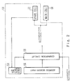
- Figure 2 shows a simplified scheme of an existing redundant circuit
- Figure 3 shows its action.
- a redundant circuit 50 has a spare cell 52, a status memory part 54, a faulty address memory part 56 and a comparison circuit 58.
- 60 is a main cell.
- the comparison signal 64 from the comparison circuit 58 for a match of the memory address and the input address is different from that for a mismatch. That is, if the memory address and the input address are in a mismatch, the comparison signal 64 shows a mismatch, i.e. "0" level, which enables the main cell 60 to be accessed. On the other hand, if the memory address and the input address are in a match, the comparison signal 64 shows a match, i.e. "1" level, which enables the spare cell 52 to be accessed.
- a redundant circuit as described above is configured by an erasable element such as a DRAM, an SRAM or an EPROM, and a check detects a failure in the redundant circuit after check data are written to the redundant circuit, there is no problem because the check data of the redundant circuit can be erased. That is, if the existence of a failure in a redundant circuit is detected after the redundant circuit (its spare cell) is checked, a processing to avoid using the redundant circuit is possible.
- the redundant circuit is configured by an unerasable element such as a PROM or a mask ROM, a check to detect a failure in the redundant circuit cannot be performed, because once check data are written to the redundant circuit (its spare cell), they cannot be erased. This prevents the data assumed to be written to the redundant circuit from being written.
- an unerasable element such as a PROM or a mask ROM
- a faulty address memory part and a status memory part are configured by a PROM.
- the faulty address memory part and the status memory part are so configured that they cannot erase or rewrite data, whether they comprise an erasable/rewritable PROM or an unerasable/unrewritable PROM.
- An example of the former is a fuse cut type PROM and an example of the latter is an EPROM memory element that is shielded from light.
- An unerasable/unrewritable PROM is used because a feared misaction, that a row or a column containing a failure gets accessed since the row or the column assumed to be replaced becomes different from the row or the column containing a failure when the redundant circuit is actually used, does not actually occur.
- a redundant circuit (its spare cell) uses an unerasable element, the redundant circuit cannot be checked by writing check data into it.
- semiconductor memory devices having multiple redundant circuits, e.g. two.
- the semiconductor memory device is operable, even if one of the two redundant circuits has a failure, if the other redundant circuit does not have a failure, since the other one could be used.
- it because it is impossible to check a redundant circuit by writing check data to it, it also becomes impossible to check which of the two redundant circuits used has a failure when two redundant circuits are used (one with a failure and the other without a failure), and it is possible for the one having a failure to be selected. In this case, the failure of the main cell is not eliminated and despite the existence of the other redundant circuit having no failure, the semiconductor memory device may remain faulty and the yield lowered.
- An object of this invention is to provide a semiconductor memory device with more than one redundant circuit, in which, when one of the redundant circuits has a failure, it can be put out of use even after programming.
- a semiconductor memory device has a first memory part and more than one redundant circuit that is used when the first memory part is faulty.
- the redundant circuits are equipped with a second memory part, a status memory part that memorizes whether the second memory part is in the in-use or the not-in-use status, a faulty address memory part that memorizes a faulty address of the first memory part, and a comparison circuit that has the second memory part get accessed in lieu of the first memory part by outputting a match signal only if the memory address from the faulty address memory part and the input address is matched after comparison when the status memory part shows the in-use status.
- the status memory part memorizes an out-of-use status meaning the second memory part has a failure. It also memorizes whether the second memory part is in the not-in-use status or the in-use status.
- the comparison circuit prohibits the second memory part from being accessed regardless of a match or a mismatch of a memory address from the faulty address memory part and the input address when the status memory part is in the out-of-use status.
- each redundant circuit the data originally assumed to be written are written (programmed) to the second memory part (spare cell), the data written into the second memory part are confirmed at this time, and the status memory part memorizes that the second memory part is in the out-of-use status, even after programming, when the existence of a failure in the second memory part is confirmed.
- the second memory part that has a failure is prohibited from being accessed regardless of a match or a mismatch of the memory address and the input address. If another redundant circuit has a second memory part (spare cell) without any failure, this second memory part is accessed when the memory address matches the input address.
- a semiconductor memory device has a first memory part and a redundant circuit that is used when the first memory part is faulty.
- the redundant circuit is equipped with more than one second memory part and more than one status memory part set corresponding to the more than one second memory part.
- the redundant circuit comprises a plurality of second memory parts, a plurality of status memory parts provided corresponding to the second memory parts and for memorizing whether the second memory parts are in the in-use status, the not-in-use status, or the out-of-use status, the out-of-use status meaning the existence of a failure in the second memory part, a faulty address memory part that memorizes a faulty address of the first memory part, and a comparison circuit that outputs a match signal only if the memory address from the faulty address memory part is matched with the input address for selecting one second memory part corresponding to the status memory part showing the in-use status, and accessing it in lieu of the first memory part when the comparison circuit outputs a match signal and one of the status memory parts is in the in-use status.
- the data originally assumed to be written are written (programmed) to more than one second memory part (spare cell).
- the data written into the second memory parts are confirmed at this time and, when the existence of a failure in any second memory part is confirmed, the corresponding status memory part memorizes that the second memory part is in the out-of-use status even after programming.
- the memory address and the input address match, a non-failed second memory part in the in-use status is selected and this second memory part is accessed in lieu of the first memory part.
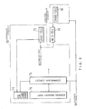
- a redundant circuit 70 contains a spare cell 72 as the second memory part, a status memory part 74, an address memory part 76 and a comparison circuit 78. 80 is the main cell as the first memory part.
- another redundant circuit 82 is established, which is configured similarly to the redundant circuit 70.
- the comparison signal 86 from the comparison circuit 78 indicates "0" level, regardless of a match or a mismatch of the memory address from the faulty address memory part 76 with the input address of the address signal 84, which enables the main cell 80 to be accessed.
- the comparison signal 86 from the comparison circuit 78 for a match of the memory address and the input address differs from that for a mismatch. That is, for a mismatch between the memory address and the input address, the comparison signal 86 indicates a mismatch, i.e. "0" level, which enables the main cell 80 to be accessed; for a match between the memory address and the input address, the comparison signal 86 indicates a match, i.e. "0" level, which enables the spare cell 72 to be accessed.
- the comparison signal 86 from the comparison circuit 78 indicates a mismatch, i.e. "0" level, regardless of whether there is a match or a mismatch between the memory address and the input address. This prohibits the spare cell 72 from getting accessed.
- the other redundant circuit 82 without a failure has a spare cell 88, i.e., if the status memory part within the redundant circuit 82 shows that the spare cell 88 is in the in-use status ("1" level), in case of a match between the memory address and the input address, the spare cell 88 without any failure gets accessed.
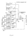
- Figure 6 shows the redundant circuit of the first preferred embodiment of this invention
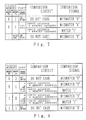
- Figure 7 shows its actions.
- the status memory part 74 contains a memory (A) 90-1 and a memory (B) 90-2 configured by a PROM, as well as an Inverter 91.
- the faulty address memory part 76 contains a memory (1) 92-1, a memory (2) 92-2, a memory (3) 92-3 and a memory (4) 92-4.
- the comparison circuit 78 contains exclusive "OR" gates (EOR) 94-1, 94-2, 94-3 and 94-4, as well as "AND” gates 96 and 98.
- An input terminal of respective EOR 94-1 through 94-4 is connected to memories 92-1 through 92-4 and the other input terminal of the same is supplied with input addresses 84-1 through 84-4 via Inverters 100-1 through 100-4.
- the memory 90-1 When the status memory part 74 indicates the in-use status, the memory 90-1 is programmed to show "1" level, whereas the memory 90-2 remains in “0" level. Therefore, in the comparison circuit 78, the input terminals 98a and 98b of the "AND” gate 98 are in “1” level, and the "AND” gate 98 is in an ON-action-ready status.
- the comparison signal 86 from the "AND” gate 98 for a match of the memory address and the input address differs from that for a mismatch.
- any respective mismatch between memory addresses 102-1 through 102-4 from memories 92-1 through 92-4 of the address memory part 76 and input addresses 84-1 through 84-4 of the address signal 84 causes the comparison signal 86 from the "AND" gate 98 to indicate a mismatch, i.e. "0" level, since the output from the "AND” gate 96, i.e. the input terminal 98c of the "AND” gate 98, is at "0" level.
- This enables the main cell 80 to be accessed.
- Figure 8 shows the redundant circuit of the second preferred embodiment of this invention
- Figure 9 shows its actions.
- memory 90-1 indicates the not-in-use status or the in-use status
- memory 90-2 indicates a usable status or the out-of-use status. Since memories 90-1 and 90-2 are independent in their roles, the use of those two memories produces four combinations. In the second embodiment shown in Figures 8 and 9, there are two use statuses. (In the first embodiment, there is only one use status.)
- the status memory part 74 realizes an in-use status 1.
- the status memory part 74 contains an EOR 104 besides memories 90-1 and 90-2; the in-use status detection part 106 contains "AND" gates 108 and 110 as well as inverters 112 and 114, and can detect whether the status memory part 74 realizes the in-use status 1 or in-use status 2.
- the status memory part 74 realizes the in-use status 1
- the in-use status 1 detection signal 116 from "AND” gate 108 realizes “1” level.
- the status memory part 74 realizes the in-use status 2
- the status memory part 74 realizes the not-in-use status.
- status memory part 74 realizes the out-of-use status and their processings are similar to those of the first embodiment.
- the redundant circuit in the second embodiment is configured to be able to change between the row side relief and the column side relief, e.g. with a mask ROM, it can memorize whether it relieves the row side or the column side as the in-use status 1 or the in-use status 2, respectively.
- Figure 10 shows an example of the system configuration of a semiconductor device in such a case.
- the in-use status detection part 106 (configured the same as that of Figure 8) outputs either the in-use status 1 detection signal 116 or the in-use status 2 detection signal 118, according to which an address switching circuit 120 changes the relief direction.
- the address switching circuit 120 changes the relief direction either in the row direction (word line direction) or in the column direction (bit line direction), respectively, when the in-use status detection part 106 outputs either the in-use status 1 detection signal 116 or the in-use status 2 detection signal 118.
- 122 is a redundant row decoder
- 124 is a redundant column decoder
- 126 is a sense amplifier
- 128 is a data switching circuit
- 130 is an input/output buffer
- 132 is an input/output signal
- 134 is a row address buffer
- 136 is a column address buffer
- 138 is a row decoder
- 140 is a column decoder
- 142 is a sense amplifier.
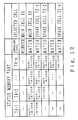
- Figure 11 shows the redundant circuit of the third preferred embodiment of this invention
- Figure 12 shows its actions.
- each of more than one redundant circuit is configured to be equipped with the spare cell 72, the status memory part 74, the faulty address memory part 76 and the comparison circuit 78.
- the more than one spare cell 72-1 through 72-n is configured to have only one piece of the faulty address memory part 76 and the comparison circuit 78. That is, shown in Figure 11, the configuration of the third embodiment is as follows.
- One piece of the redundant circuit 70 has more than one spare cell 72-1 through 72-n and more than one status memory part 74-1 through 74-n, each set to correspond to one of the spare cells 72-1 through 72-n.
- the newly set selection circuit 150 properly selects one spare cell to be accessed among the more than one spare cell 72-1 through 72-n, according to the memory content of each of the status memory parts 74-1 through 74-n and the comparison signal from the comparison circuit 78.
- This configuration produces the action shown in Figure 12. That is, if the memory address 102 of the faulty address memory part 76 and the input address 84 match, and the comparison circuit 78 outputs a matching signal, and any of the status memory parts 74-1 through 74-n show the in-use status, the selection circuit 150 selects one spare cell to correspond to the status memory part that shows the in-use status, and this spare cell is accessed in lieu of the main cell 80. However, even if the comparison circuit 78 outputs a matching signal, unless any of the status memory parts 74-1 through 74-n shows the in-use status, the main cell 80 is selected.
- the comparison circuit 78 does not output a matching signal (in case of a mismatch), regardless of the content of the status memory parts 74-1 through 74-n, the main cell 80 is selected.
- the selection circuit 150 is prohibited from selecting the spare cell.
- this invention puts the failed spare cell in the out-of-use status. Then, if another spare cell does not have a failure, the spare cell without a failure is put into use. Therefore, this invention improves the yield of a semiconductor memory device.
Landscapes
- For Increasing The Reliability Of Semiconductor Memories (AREA)
- Techniques For Improving Reliability Of Storages (AREA)
Applications Claiming Priority (2)
| Application Number | Priority Date | Filing Date | Title |
|---|---|---|---|
| JP240957/89 | 1989-09-18 | ||
| JP1240957A JPH03104097A (ja) | 1989-09-18 | 1989-09-18 | 半導体記憶装置 |
Publications (2)
| Publication Number | Publication Date |
|---|---|
| EP0423495A2 true EP0423495A2 (de) | 1991-04-24 |
| EP0423495A3 EP0423495A3 (en) | 1992-10-21 |
Family
ID=17067167
Family Applications (1)
| Application Number | Title | Priority Date | Filing Date |
|---|---|---|---|
| EP19900117849 Ceased EP0423495A3 (en) | 1989-09-18 | 1990-09-17 | A semiconductor memory device |
Country Status (4)
| Country | Link |
|---|---|
| US (1) | US5195057A (de) |
| EP (1) | EP0423495A3 (de) |
| JP (1) | JPH03104097A (de) |
| KR (1) | KR940006920B1 (de) |
Cited By (1)
| Publication number | Priority date | Publication date | Assignee | Title |
|---|---|---|---|---|
| EP0763794A3 (de) * | 1995-09-18 | 1999-04-14 | Nec Corporation | Halbleiterspeicher und Verfahren zum Ersetzen einer redundanten Speicherzelle |
Families Citing this family (41)
| Publication number | Priority date | Publication date | Assignee | Title |
|---|---|---|---|---|
| JPH05500724A (ja) * | 1989-07-06 | 1993-02-12 | エムブイ リミテッド | 障害許容データ記憶システム |
| US5398206A (en) * | 1990-03-02 | 1995-03-14 | Hitachi, Ltd. | Semiconductor memory device with data error compensation |
| JP2778234B2 (ja) * | 1990-09-13 | 1998-07-23 | 日本電気株式会社 | 冗長デコーダ回路 |
| JPH04192198A (ja) * | 1990-11-27 | 1992-07-10 | Mitsubishi Electric Corp | 冗長回路 |
| JP2687785B2 (ja) * | 1991-09-27 | 1997-12-08 | 日本電気株式会社 | 半導体記憶装置 |
| US5257229A (en) * | 1992-01-31 | 1993-10-26 | Sgs-Thomson Microelectronics, Inc. | Column redundancy architecture for a read/write memory |
| JPH05242693A (ja) * | 1992-02-28 | 1993-09-21 | Mitsubishi Electric Corp | 半導体記憶装置 |
| JP3268823B2 (ja) * | 1992-05-28 | 2002-03-25 | 日本テキサス・インスツルメンツ株式会社 | 半導体記憶装置 |
| US6000843A (en) * | 1992-07-03 | 1999-12-14 | Nippon Steel Corporation | Electrically alterable nonvolatile semiconductor memory |
| JP2922060B2 (ja) * | 1992-07-27 | 1999-07-19 | 富士通株式会社 | 半導体記憶装置 |
| US5471479A (en) * | 1992-08-06 | 1995-11-28 | Motorola, Inc. | Arrangement for column sparing of memory |
| JP3020077B2 (ja) * | 1993-03-03 | 2000-03-15 | 株式会社日立製作所 | 半導体メモリ |
| GB9305801D0 (en) * | 1993-03-19 | 1993-05-05 | Deans Alexander R | Semiconductor memory system |
| US5386380A (en) * | 1993-07-21 | 1995-01-31 | United Microelectronics Corporation | Bypass scheme for ROM IC |
| US5404331A (en) * | 1993-07-30 | 1995-04-04 | Sgs-Thomson Microelectronics, Inc. | Redundancy element check in IC memory without programming substitution of redundant elements |
| EP0657814B1 (de) * | 1993-12-07 | 1999-03-17 | STMicroelectronics S.r.l. | Halbleiterspeicher mit redundanter Schaltung |
| JP2751821B2 (ja) * | 1994-02-16 | 1998-05-18 | 日本電気株式会社 | 不揮発性半導体記憶装置 |
| DE9412376U1 (de) * | 1994-08-01 | 1995-12-07 | TELBUS Gesellschaft für elektronische Kommunikations-Systeme mbH, 85391 Allershausen | Speicherschaltung zur Kompensation von Bitfehlern in Speicherbausteinen |
| US5572470A (en) * | 1995-05-10 | 1996-11-05 | Sgs-Thomson Microelectronics, Inc. | Apparatus and method for mapping a redundant memory column to a defective memory column |
| US5644541A (en) * | 1995-11-03 | 1997-07-01 | Philip K. Siu | Memory substitution system and method for correcting partially defective memories |
| US5631868A (en) * | 1995-11-28 | 1997-05-20 | International Business Machines Corporation | Method and apparatus for testing redundant word and bit lines in a memory array |
| US5640353A (en) * | 1995-12-27 | 1997-06-17 | Act Corporation | External compensation apparatus and method for fail bit dynamic random access memory |
| US5771195A (en) * | 1995-12-29 | 1998-06-23 | Sgs-Thomson Microelectronics, Inc. | Circuit and method for replacing a defective memory cell with a redundant memory cell |
| US5841709A (en) * | 1995-12-29 | 1998-11-24 | Stmicroelectronics, Inc. | Memory having and method for testing redundant memory cells |
| US6037799A (en) * | 1995-12-29 | 2000-03-14 | Stmicroelectronics, Inc. | Circuit and method for selecting a signal |
| US5790462A (en) * | 1995-12-29 | 1998-08-04 | Sgs-Thomson Microelectronics, Inc. | Redundancy control |
| US5612918A (en) * | 1995-12-29 | 1997-03-18 | Sgs-Thomson Microelectronics, Inc. | Redundancy architecture |
| JP3244031B2 (ja) * | 1997-08-20 | 2002-01-07 | 日本電気株式会社 | 半導体記憶装置 |
| US6034891A (en) * | 1997-12-01 | 2000-03-07 | Micron Technology, Inc. | Multi-state flash memory defect management |
| US6536005B1 (en) * | 1999-10-26 | 2003-03-18 | Teradyne, Inc. | High-speed failure capture apparatus and method for automatic test equipment |
| KR100380024B1 (ko) * | 2001-01-04 | 2003-04-18 | 삼성전자주식회사 | 리던던시를 구비하는 반도체 메모리 장치 |
| JP4062247B2 (ja) * | 2003-12-11 | 2008-03-19 | ソニー株式会社 | 半導体記憶装置 |
| US7035152B1 (en) * | 2004-10-14 | 2006-04-25 | Micron Technology, Inc. | System and method for redundancy memory decoding |
| JP2006345912A (ja) * | 2005-06-13 | 2006-12-28 | Young Sangyo Co Ltd | バッグのポケット構造 |
| JP2007081018A (ja) * | 2005-09-13 | 2007-03-29 | Matsushita Electric Ind Co Ltd | 電気ヒューズモジュール |
| US9229887B2 (en) * | 2008-02-19 | 2016-01-05 | Micron Technology, Inc. | Memory device with network on chip methods, apparatus, and systems |
| US8086913B2 (en) * | 2008-09-11 | 2011-12-27 | Micron Technology, Inc. | Methods, apparatus, and systems to repair memory |
| US9123552B2 (en) | 2010-03-30 | 2015-09-01 | Micron Technology, Inc. | Apparatuses enabling concurrent communication between an interface die and a plurality of dice stacks, interleaved conductive paths in stacked devices, and methods for forming and operating the same |
| US8887013B2 (en) * | 2011-07-01 | 2014-11-11 | Avalanche Technology, Inc. | Mapping of random defects in a memory device |
| US9472302B2 (en) * | 2013-03-07 | 2016-10-18 | Intel Corporation | Redundant fuse coding |
| US11099748B1 (en) * | 2018-08-08 | 2021-08-24 | United States Of America As Represented By The Administrator Of Nasa | Fault tolerant memory card |
Family Cites Families (5)
| Publication number | Priority date | Publication date | Assignee | Title |
|---|---|---|---|---|
| US4639897A (en) * | 1983-08-31 | 1987-01-27 | Rca Corporation | Priority encoded spare element decoder |
| JP2530610B2 (ja) * | 1986-02-27 | 1996-09-04 | 富士通株式会社 | 半導体記憶装置 |
| JPS62204499A (ja) * | 1986-03-04 | 1987-09-09 | Oki Electric Ind Co Ltd | メモリ装置の冗長回路 |
| FR2611400A1 (fr) * | 1987-02-26 | 1988-09-02 | Thomson Semiconducteurs | Procede de test d'elements pour une memoire integree et dispositif de mise en oeuvre du procede |
| JPS63244494A (ja) * | 1987-03-31 | 1988-10-11 | Toshiba Corp | 半導体記憶装置 |
-
1989
- 1989-09-18 JP JP1240957A patent/JPH03104097A/ja active Pending
-
1990
- 1990-09-17 EP EP19900117849 patent/EP0423495A3/en not_active Ceased
- 1990-09-18 US US07/584,311 patent/US5195057A/en not_active Expired - Lifetime
- 1990-09-18 KR KR1019900014703A patent/KR940006920B1/ko not_active Expired - Fee Related
Cited By (1)
| Publication number | Priority date | Publication date | Assignee | Title |
|---|---|---|---|---|
| EP0763794A3 (de) * | 1995-09-18 | 1999-04-14 | Nec Corporation | Halbleiterspeicher und Verfahren zum Ersetzen einer redundanten Speicherzelle |
Also Published As
| Publication number | Publication date |
|---|---|
| US5195057A (en) | 1993-03-16 |
| KR940006920B1 (ko) | 1994-07-29 |
| KR910006999A (ko) | 1991-04-30 |
| JPH03104097A (ja) | 1991-05-01 |
| EP0423495A3 (en) | 1992-10-21 |
Similar Documents
| Publication | Publication Date | Title |
|---|---|---|
| US5195057A (en) | Semiconductor memory device having a redundant memory which can be selectively placed in a not-in-use status | |
| JP2530610B2 (ja) | 半導体記憶装置 | |
| US5124948A (en) | Mask ROM with spare memory cells | |
| KR950009743A (ko) | 다른칩에 구제기능을 가진 반도체 메모리 시스템 | |
| JP3594891B2 (ja) | 半導体記憶装置およびその検査方法 | |
| KR950008541B1 (ko) | 반도체 기억장치의 용장회로 | |
| US6314030B1 (en) | Semiconductor memory having segmented row repair | |
| US6434067B1 (en) | Semiconductor memory having multiple redundant columns with offset segmentation boundaries | |
| US6041422A (en) | Fault tolerant memory system | |
| WO2001016955A1 (en) | Circuit and method for a multiplexed redundancy scheme in a memory device | |
| JP4504558B2 (ja) | 半導体集積メモリ | |
| KR960011542B1 (ko) | 반도체 메모리 장치 | |
| JP2619170B2 (ja) | 半導体メモリ及びその試験方法 | |
| EP0472209B1 (de) | Halbleiterspeichergerät mit Redundanzschaltung | |
| US5025418A (en) | Semiconductor device for performing automatic replacement of defective cells | |
| US5058071A (en) | Semiconductor memory device having means for repairing the memory device with respect to possible defective memory portions | |
| JP3281203B2 (ja) | 半導体記憶装置 | |
| US6320791B1 (en) | Writing apparatus for a non-volatile semiconductor memory device | |
| US6421283B1 (en) | Trap and patch system for virtual replacement of defective volatile memory cells | |
| JP3866345B2 (ja) | 半導体記憶装置及び半導体記憶装置の試験方法 | |
| KR100924579B1 (ko) | 리던던시 메모리 셀 억세스 회로, 이를 포함하는 반도체메모리 장치, 및 반도체 메모리 장치의 테스트 방법 | |
| JPH01133298A (ja) | 半導体メモリ装置 | |
| US6373759B2 (en) | SRAM device | |
| JP2973419B2 (ja) | 半導体メモリ装置 | |
| JPH03160698A (ja) | 不揮発性半導体記憶装置 |
Legal Events
| Date | Code | Title | Description |
|---|---|---|---|
| PUAI | Public reference made under article 153(3) epc to a published international application that has entered the european phase |
Free format text: ORIGINAL CODE: 0009012 |
|
| AK | Designated contracting states |
Kind code of ref document: A2 Designated state(s): DE FR GB |
|
| PUAL | Search report despatched |
Free format text: ORIGINAL CODE: 0009013 |
|
| AK | Designated contracting states |
Kind code of ref document: A3 Designated state(s): DE FR GB |
|
| 17P | Request for examination filed |
Effective date: 19930323 |
|
| 17Q | First examination report despatched |
Effective date: 19950608 |
|
| STAA | Information on the status of an ep patent application or granted ep patent |
Free format text: STATUS: THE APPLICATION HAS BEEN REFUSED |
|
| 18R | Application refused |
Effective date: 19951201 |