EP0423940A2 - Logische Schaltung - Google Patents
Logische Schaltung Download PDFInfo
- Publication number
- EP0423940A2 EP0423940A2 EP90310171A EP90310171A EP0423940A2 EP 0423940 A2 EP0423940 A2 EP 0423940A2 EP 90310171 A EP90310171 A EP 90310171A EP 90310171 A EP90310171 A EP 90310171A EP 0423940 A2 EP0423940 A2 EP 0423940A2
- Authority
- EP
- European Patent Office
- Prior art keywords
- transistor
- emitter
- power source
- output
- base
- Prior art date
- Legal status (The legal status is an assumption and is not a legal conclusion. Google has not performed a legal analysis and makes no representation as to the accuracy of the status listed.)
- Withdrawn
Links
Images


Classifications
-
- H—ELECTRICITY
- H03—ELECTRONIC CIRCUITRY
- H03K—PULSE TECHNIQUE
- H03K19/00—Logic circuits, i.e. having at least two inputs acting on one output; Inverting circuits
-
- H—ELECTRICITY
- H03—ELECTRONIC CIRCUITRY
- H03K—PULSE TECHNIQUE
- H03K19/00—Logic circuits, i.e. having at least two inputs acting on one output; Inverting circuits
- H03K19/01—Modifications for accelerating switching
- H03K19/013—Modifications for accelerating switching in bipolar transistor circuits
- H03K19/0136—Modifications for accelerating switching in bipolar transistor circuits by means of a pull-up or down element
-
- H—ELECTRICITY
- H03—ELECTRONIC CIRCUITRY
- H03K—PULSE TECHNIQUE
- H03K19/00—Logic circuits, i.e. having at least two inputs acting on one output; Inverting circuits
- H03K19/02—Logic circuits, i.e. having at least two inputs acting on one output; Inverting circuits using specified components
- H03K19/08—Logic circuits, i.e. having at least two inputs acting on one output; Inverting circuits using specified components using semiconductor devices
- H03K19/082—Logic circuits, i.e. having at least two inputs acting on one output; Inverting circuits using specified components using semiconductor devices using bipolar transistors
- H03K19/086—Emitter coupled logic
Definitions
- This invention relates to logic circuits and in particular to emitter coupled logic (ECL) circuits.
- ECL emitter coupled logic
- ECL circuits are often used as logic circuits in high performance systems such as large-sized computers, work stations, and measuring instruments due to their high speed characteristics. With recent improvements in system performance, ECL logic circuits are required to be higher in speed and integration density. But the greater the integration, the greater the power consumption and the more the delay in long wiring cannot be ignored . Therefore it is necessary to realize a low power consumption and high-speed operation of the circuit in long wiring.
- ECL logic circuits are high-speed digital circuits composed of a current mode logic (CML) circuit and emitter-follower transistor added to improve the load driving capacity.
- CML current mode logic
- V ref central voltage value of logical amplitude
- the output voltage is characterized in that both positive and negative outputs (OR and NOR logical outputs) can be taken out.
- the charging and discharging time of charges accumulated in this wiring load capacitance CL is one of the factors determining the circuit operation speed. If the wiring load capacitance CL is large, it takes the output a longer time to change from the H level to the L level than from L level to the H level.
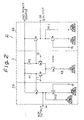
- FIG. 1 denotes an active pull-down ECL logic circuit (OR/NOR circuit) which consists of the CML circuit (ECL logic part) 2 made of emitter-coupled transistors Q1 and Q2, a constant current transistor Q3, resistors R1, R2, and R3; the emitter-follower circuit 3 made of an emitter-follower transistor Q4, pull-down transistor Q5, and emitter-follower resistor R4; and the emitter-follower circuit 4 made of an emitter-follower transistor Q6, pull-down transistor Q7, and emitter-follower resistor R5.
- CML circuit ECL logic part
- R1, R2, and R3 constant current transistor
- the emitter-follower circuit 3 made of an emitter-follower transistor Q4, pull-down transistor Q5, and emitter-follower resistor R4
- the emitter-follower circuit 4 made of an emitter-follower transistor Q6, pull-down transistor Q7, and emitter-follower resistor R5.
- the base of pull-down transistor Q5 is connected to the collector of the transistor Q1 via a capacitor C1, whose signals are inversed in phase to the signals applied to the base of the emitter-follower transistor Q4.
- the base of the pull-down transistor Q7 is connected to the collector of the transistor Q2 via a capacitor C2, whose signals are inversed in phase to the signals applied to the base of the emitter-follower transistor Q6.
- numerals 11 and 12 denote the input terminals where input signals Vin1 and Vin2 are input
- 13 and 14 denote the output terminals from which the output signals Vout1 and Vout2 are output.
- Vcs1 is the control voltage
- GND the high potential power source
- V EE1 the low potential power source (negative power source).
- the NPN transistor Q5 is usually on when sending the output level from the output terminal 13, and when Q5 changes, its current flow is instuntaneously increased by the current flowing through the capacitor C1.
- the control voltage V cs1 is always applied to the bases of Q5 and Q7 to turn them on in order to produce the output level. Only when Q5 and Q7 are changed is the current flowing through them increased by the current momentarily flowing through the capacitors C1 and C2 (which block DC) to improve the load driving force. Then the charges are promptly discharged from the wiring load capacitance CL via Q5, resistor R4, Q7, and resistor R5 to switch from the level H to the level L at high speed.
- Vcs1 In the active pull-down ECL logic circuit of Figure 1, however, Vcs1 must be applied to the transistors Q5 and Q7 at all times to keep them turned on, which results in increased power consumption, making it necessary to increase the transistor size.
- the increased junction and wiring capacity can obstruct high speed operation while the increased gate size prevents high integration of transistors.
- a logic circuit, especially an ECL logic circuit, embodying the present invention comprises a logic circuit containing an emitter-coupled transistor which is composed of first and second transistors, the collectors of which are both connected to a second power source and the emitters of which are commonly connected to a constant current source connected to a first power source.
- Input signals are input to the base of each transistor and the output signal in the same or inverse phase as the input signals output from each collector of both transistors; an output circuit comprising an emitter-follower transistor having its base connected to the collector of at least one transistor of the logic circuit having its collector connected to a second power source and having its emitter connected to an output terminal; a pull-down transistor having its collector connected to the emitter of the emitter-follower transistor and its emitter connected to a third power source; a control voltage terminal which is connected to the base of the pull-down transistor and a pulse greater than the threshold voltage of the pull-down transistor is input at the instant the logic level at the output terminal changes from high to low.
- a resistor which is inserted between the emitter-follower transistor and a fourth power source.
- resistors R11 and R12 are inserted between emitter-follower transistors Q4 and Q6 of the emitter circuit and a fourth power source V EE2.
- the emitter-follower current flowing through the transistors Q5 and Q7 flow through the resistors R11 and R12, and Q5 and Q7 are normally in an off-state.
- the pulse higher than the threshold voltage is input to the base of the transistors Q5 and Q7 and they operate to actively lower the output voltage level.
- it becomes possible to make the circuitry operate at a high speed because the discharge time of charges accumulated in a load capacitance of the circuit is reduced, while the power consumption of the circuit can be maintained at a desirably low level even if the wiring load is large.
- FIG. 2 is a circuit diagram of an ECL logic output circuit embodying the present invention, in which the same numbers are given to components which correspond to the same components in the previously-considered circuit shown in Fig. 1.
- numeral 21 shows an active pull-down ECL logic circuit (ECL logic circuit).
- This circuit 21 is composed of a CML circuit (ECL logic circuit) 2 consisting of emitter-coupled transistors Q1 and Q2, constant current transistor Q3, resistors R1, R2, and R3; an emitter-follower circuit (OR output) 22 for receiving signals from the transistor Q2 and driving an external load; and an emitter-follower circuit (NOR output) 23 for receiving signals from Q1 and driving an external load.
- CML circuit ECL logic circuit 2 consisting of emitter-coupled transistors Q1 and Q2, constant current transistor Q3, resistors R1, R2, and R3
- an emitter-follower circuit (OR output) 22 for receiving signals from the transistor Q2 and driving an external load
- an emitter-follower circuit (NOR output) 23 for receiving signals from Q1 and driving an external load.
- the emitter-follower circuit 23 comprises an emitter-follower transistor Q6, the base of which is connected to the collector of the emitter-coupled transistor Q1 of ECL logic circuit 2, the collector of which is connected to a second power source, and the emitter of which is connected to an output terminal 14 (NOR); a pull-down transistor Q7 the collector of which is connected to the emitter of the emitter-follower transistor Q6 and the emitter of which is connected to a third power source; a control voltage terminal 16 connected to the base of the pull-down transistor Q7 and receiving a pulse higher than the threshold voltage of the pull-down transistor Q7 at the instant the logic level at the output terminal 14 changes from high to low ; and resistor R12 inserted between the collector of pull-down transistor Q7 and a fourth power source.
- Q5 and Q7 can normally be kept off and the current flows from the emitter-follower through the resistors R11 and R12. Namely, current usually flows through R11 (or R12) while keeping the transistor Q5 (and Q7) turned off.
- the emitter-follower output circuits 22 and 23 were arranged to connect to the respective outputs from the ECL logic circuit 2, but only one emitter-follower circuit may be used.
- Circuitry embodying the invention can be used when two outputs (such as OR/NOR, or AND/NAND) are obtained at once from the ECL logic circuit.
- a circuit as shown in Fig. 7, for example, can be used to detect the timing when the output from the emitter-follower output circuit changes from “H” to "L”, and generate a pulse to be applied to either control voltage terminal 15 or 16, thereby momentarily turning on the corresponding pull-down transistor Q5 or Q7 and discharging the charges from the load connected to the output 13 through the transistor Q5 or Q7, thus considerably improving the switching operation of the circuit.
- the first and third power sources may be the same power supply rail.
- FIGs 3 through 6 relate to a first embodiment of an ECL logic circuit according to the aforesaid principle.
- the same reference numerals are given to the same components as in the circuitry of Figs. 1 and 2.
- numeral 31 shows an active pull-down ECL logic circuit (ECL logic circuit), which comprises a CML circuit (ECL logic) 2 consisting of an emitter-coupled transistor Q3 and resistors R1, R2, and R3; an emitter-follower circuit (OR output part) 32 for receiving the signals appearing at the transistor Q2 and driving an external load; and an emitter-follower circuit (NOR output part) 33 for receiving the signals from the transistor Q1 and driving an external load.
- ECL logic circuit active pull-down ECL logic circuit
- CML circuit ECL logic 2 consisting of an emitter-coupled transistor Q3 and resistors R1, R2, and R3
- an emitter-follower circuit OR output part
- NOR output part for receiving the signals from the transistor Q1 and driving an external load.
- the emitter-follower circuit 32 comprises an emitter-follower transistor Q4 receiving the Q2 collector potential at its base; a pull-down transistor Q5, the collector of which is connected to the emitter of the emitter-follower transistor Q4, and the base of which is connected via the capacitor C1, to the collector of the emitter-coupled transistor Q1, whose output is inversed in phase to that at the base of emitter-follower transistor Q4, and at the same time, is connected to a fifth power source via a level shift means 34 consisting of a transistor, diode, resistor etc.; and a resistor R11 inserted between the emitter-follower transistor Q4 and the fourth power source.
- a level shift means 34 consisting of a transistor, diode, resistor etc.
- the emitter-follower circuit 33 comprises an emitter-follower transistor Q6 receiving the Q1 collector potential at its base; a pull-down transistor Q7, the collector of which is connected to the emitter of the emitter-follower transistor Q6, and the base of which is connected via the capacitor C2, to the collector of emitter-coupled transistor Q2, whose output is inversed in phase to that at the base of emitter-follower transistor Q6, and at the same time is connected to a fifth power source via the level shift means consisting of a transistor, diode, resistor, etc.; and a resistor R12 inserted between the emitter-follower transistor Q6 and a fourth power source. Therefore the active pull down ECL logic circuit 31 has a circuit construction wherein resistors R11 and R12 provide respective current paths essentially in parallel with the major current paths of the transistors Q5 and Q7.
- the capacitors C1 and C2 in this embodiment are equivalent to the aforesaid control voltage generating means.
- the emitters of Q4 and Q6 are connected to a fourth power source V EE2 via resistors R11 and R12.
- the transistors Q5 and Q7 can normally be kept off by allowing the emitter-follower current to flow through resistors R11 and R12.
- the DC emitter-follower current flows through R11 (or R12) when the transistors Q5 (and Q7) are off. But when the output is changed from “H” to "L”, a short signal (pulse) higher than the threshold voltage V BE between the base and emitter of Q5 is generated at the capacitor C1 (or C2), and is applied to the transistor Q5 (or Q7) to operate it to actively lower the output voltage level. Namely, the emitter-follower current normally flows through resistor R11 (and R12) (in the case of DC) and transistors Q5 (and Q7) are turned off.
- low power consumption can be achieved by using the first and fourth power sources, and making the latter which is connected to R11 and R12 less negative in potential than the former.
- the power consumption cannot be reduced, but the wiring for the two power sources can be combined into one. Since AC current flows through the capacitor C1 (or C2) connected to the transistor Q5 (or Q7) at the time of switching, the transistor Q5 (or Q7) operates to positively lower the voltage level.
- the first power source has the lowest potential while the second power source is has the highest potential in the circuit.
- the second power source may be connected to earth (GND), and thus the first power source may have a certain negative voltage, for example, - 5 V.
- the fourth power source must have a potential higher than that of the third power source while less than that of the second power source.
- the third power source may have the same potential as that of the fifth power source and therefore the third power source may be commonly used for the fifth power source and vice-versa.
- Figure 4 (a) shows a schematic circuit diagram of the emitter-follower portion 3 of the active pull-down ECL logic circuit of Fig. 1
- Fig. 4(b) shows schematically the corresponding emitter-follower portion 32 of the active pull-down ECL logic circuit of Fig. 3.
- a control voltage V CS1 applied to transistor Q5 must be at a potential that will keep Q5 turned on in order to produce the output voltage V OH /V OL .
- the power consumption thus becomes V EE1 x i with i being the emitter-follower current.
- a resistor R11 is inserted between the emitter of emitter-follower transistor Q4 and a negative power source V EEZ (a fourth power source) to generate the output voltage V ON /V OL .
- V CS1 in the Fig. 4(b) circuit is set lower than Vcs1 in Fig. 4(a), the transistor Q5 is normally off.
- the emitter /collector current in Q4 (IQ4) is equal to the emitter /collector current in Q5 (IQ5).
- the transistor Q5 can be reduced in size in proportion to the amount of the current flowing through resistor R11.
- the resistor used in a usual ECL circuit can be used for R11 and R12.
- the circuit is used where the cut-off frequency f T is low as shown in Fig.5 1, since the Q5 collector current Ic is large.
- the transistor size has to be large leading to the increased function and wiring capacities and the lowered operation speed or otherwise the increased gate size.
- circuit 21 in the present embodiment there is no problem in the circuit 21 in the present embodiment as it can be used at the place where f T is high as shown in Fig. 5 2.
- this embodiment has the effect of allowing circuit operation at high speed in order to actively lower the voltage level even if the wiring load CL is large. Further the circuit can considerably contribute to reduced power consumption because the transistor Q5 (and Q7) is normally kept off, and a fourth power source V EE2 is used to make the current flow through resistor R11 (and R12).
- the transistor Q5 or Q7 can be made smaller in size than the transistor used in the conventional circuit, and therefore is more advantageous for high integration.
- the voltage applied to the emitter-follower transistor Q4 and the inverse phase of the voltage applied to the base of pull-down transistor Q5 are obtained from the collector of each transistor of the ECL logic circuit. Since these voltages are applied via a capacitor, transient signals occur in inverse phase relative to the input signals, which can shorten the turn-on time of the pull-down transistor.
- the input 11 can be replaced by multiple inputs.
- Figure 7 is a circuit diagram of another embodiment of an ECL logic circuit according to the present invention, showing a circuit for generating a control voltage to be applied to the base of pull-down transistor Q5 or Q7 of the ECL logic circuit 21 shown in Fig. 2. Only the part where the control voltage output is input to the ECL logic circuit is different from the circuit in Fig. 2, so the identical circuit construction is omitted and only the main part will be explained.
- this circuit does not derive a Q1 or Q2 collector potential from the ECL logic 2 via capacitors C1 and C2, but incorporates a transistor Q8 and resistors R13 and R14 into the input section of ECL logic part 2 as shown in Fig. 7, and connects the collector and emitter of transistor Q8 to the bases of OR pull-down transistor Q5 and NOR pull-down transistor Q7 via capacitors C3 and C4, respectively.
- pulses take place from capacitor C3 or C4 depending on changes in input, and are applied instuntaneously to the bases of pull-down transistors Q5 and Q7.
- the subsequent circuit operations are the same as in the circuit of the first embodiment.
- the circuit construction is shown of a control voltage generating means which simultaneously controls the pull-down transistor Q5 of the OR output section 2 and the pull-down transistor Q7 of the NOR output section 23.
- this embodiment can adopt a construction that controls the pull-down transistor of either the OR output section 22 or the NOR output section 23.
- Figure 16 shows the control voltage generating circuit developed by improving the above-mentioned control voltage generating means.
- Figure 16 shows an input circuit section (pulse generating circult) consisting of a transistor Q8, resistors R13 and R14, with the OR output section 22 being used as an active pull-down, to which is added a speed-up capacitor C113 to improve the operation speed.
- the speed-up capacitor C113 is added to both ends of resistor R14 at the emitter side of transistor Q8.
- the AC impedance can be reduced and transient current can be made to flow through the capacitor C113, so that a pulse can quickly be generated and applied to the base of active pull-down transistor Q5. Therefore the higher the input signal frequency is, the greater the effect of capacitor 113 becomes.
- this capacitor C113 is only effective when accelerating the OR output.
- this speed-up capacitor C113 is chosen according to the added wiring capacity CL for the following reasons.
- the speed-up capacitor C113 should have an appropriate value according to the added wiring capacity CL.
- this speed-up capacitor C113 is made variable according to the added wiring capacity CL, and it is small, the speed-up capacitor can be made zero or a very small value, and if the capacitor CL is large, the speed-up capacitor can be increased.
- a variable speed-up capacitor C113 can be realized by arranging a plurality of capacitors and connecting them with conductive wires.
- Figure 17 shows another embodiment of the control voltage generating circuit according to the present invention. A circuit for two inputs with the NOR side being used for active pull-down is shown.
- the collector and emitter of a transistor Q121 are commonly connected to the collector and emitter of the input side transistor Q1 of the ECL circuit, and its base is connected to another input terminal 122.
- the base of Q1 is connected to the input terminal 11 and the base of Q8.
- the input terminals 122 and 11 are connected to the bases of transistors Q128 and Q8 respectively, with their collectors connected to the second power source and their emitters to the first or third power sources via resistor R14.
- the input terminals can be increased accordingly in the same manner.
- This circuit operates in such a manner that when any one of the plural input signals is changed from the L level to the H level, one of the input transistors Q121 and Q1 of the ECL circuit where the signal is input turns on and the output terminal 13 changes from the H level to the L level.
- one of the transistors Q128 and Q8 where the signal is input turns on, and a pulse is generated by the circuit comprising the capacitors C4 and resistor R124, to turn on the pull-down transistor Q5.
- Figure 18 shows another embodiment of the control voltage generating circuit according to the present invention.
- the simple resistor at the emitter side of transistor Q8 of the circuit where the pulse is taken out is replaced with a constant current source consisting of a transistor Q159 and resistor R14.
- a voltage is applied to a terminal 153 so that the transistor Q159 is turned on.
- the voltage applied to this terminal 153 may be the same as the voltage applied to a terminal 154 (Vcs).
- the transistor Q159 as a constant current source, the current flowing through the resistor R14 can be kept constant, so that the voltage applied to the capacitor C4 can be stabilized against changes in the power source voltage, and the amplitude of the generated current can be fixed.
- circuit according to this embodiment is effective when the output is at the NOR side only.
- Figure 19 shows another embodiment of the control voltage generating circuit according to the present invention.
- an additional emitter-follower transistor Q88 and resistor R88 are added to the input circuit section consisting of R13, Q8, and R14 as mentioned above.
- the voltage changes of input signals in the transistor Q8 of the first-stage input circuit can further be amplified by the transistor Q88 of the second-stage input circuit, so as to reliably turn on the pull-down transistor Q5.
- Figure 20 shows a different embodiment of the control voltage generating circuit according to this invention, in which the input circuit in each of the above-mentioned embodiments was modified to have the same circuit construction with the ECL logic circuit.
- the input circuit construction is the same ECL circuit construction comprising transistors Q1 and Q2, and has a current switch circuit comprised of transistors Q8 and Q8′, resistors R13 and R13′.
- the constant current source of the ECL circuit at the input circuit side is comprised of transistor Q3′ and resistor R5′, and the base of transistor Q3′ is so made to have the same level as the constant current source Vcs of the ECL circuit.
- input signals are input to the base of the transistor Q8 of the input circuit via input terminal 11, and are also applied to the base of Q1 of another ECL circuit. Both the ECL circuits operate as ordinary ECL circuits.
- the voltage at the collector side of transistor Q8′ also changes from the L level to the H level and a positive pulse is generated by the differential circuit comprised of the capacitor C3 and resistor R114.
- the collector of transistor Q8′ and the base of pull-down transistor Q5 at the NOR side output circuit are connected to each other via a capacitor, but the collector of transistor Q8 may instead be connected to the base of pull-down transistor Q7 in the OR side output circuit section via a capacitor. Further, both connections can simultaneously be made.
- transistors Q74 and Q75 for supplying the pull-down transistor Q5 with DC bias are connected in series with the base of transistor Q5, but these transistors Q74 and Q75 may be removed and the pull-down transistor Q5 may be driven without using DC bias.
- this embodiment can be used when reducing the required space on the device surface is more important than the circuit operation speed.
- no capacitor is attached to the collectors of transistors Q1 and Q2 of the ECL logic section 2, so the circuit operation can be further accelerated, further enhancing the effects of the above embodiments.
- FIG. 8 shows the third embodiment of the the ECL logic output circuit according to the present invention.
- the same reference numerals are given to the same components as in the first embodiment in Figure 3, and the explanation of identical parts is omitted.
- numeral 41 denotes an active pull-down ECL circuit, which has the same circuit construction as the aforesaid active pull-down ECL logic circuit 31 except for NPN transistors Q9 and Q10, the bases of which connected to a bias voltage terminal for a constant current source (not shown), provided between the second power source (GND) and the first power source (V EE1 ), to keep their voltage level constant relative to the first power source V EE1 , and resistors R21 and R22 connected to the emitters of NPN transistors Q9 and Q10.
- Numerals 42 and 43 are emitter-follower circuits in the ECL logic circuit 41.
- this embodiment can further enhance the effects of the first embodiment.
- the logic circuit can actively lower its output voltage level while preventing an increase in power consumption, thus contributing to increased operation speed and high integration of the circuit.
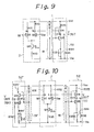
- Figure 9 shows another embodiment of a logic output circuit according to the present invention, the basic construction of which comprises a logic circuit 2 containing an emitter-coupled transistor which is composed of first and second transistors the collectors of which are both connected to the second power source, and the emitters of which are commonly connected to the constant current source connected to the first power source, an input signal in the same or inverse phase of input signals taken out from each one of collectors of different transistors; an emitter-follower transistor, the base of which is connected to the collector of at least one transistor of the logic circuit, the collector of which is preferably connected to the second power via a first resistor R15, and the emitter of which is connected to the output terminal; and a pull-down transistor, the collector of which is connected to the emitter of the emitter-follower transistor and the emitter of which is connected to the third power source.
- a logic circuit 2 containing an emitter-coupled transistor which is composed of first and second transistors the collectors of which are both connected to the second power source, and the emitters of which are
- the logic output circuit has a second resistor provided between the output terminal and the third power source, and a capacitor for connecting the collector of the emitter-follower transistor to the base of the pull-down transistor.
- the logic circuit 2 has a differential circuit formed by two transistors Q11 and Q12, and resistors R111 and R112 connected to a high potential power source Vcc (a second power source), and the emitters of transistors Q11 and Q12 are connected to a low potential power source V EE (a first power source through a resistor R113).
- Vcc a high potential power source
- V EE a low potential power source through a resistor R113.
- the base of transistor Q11 is used as the input IN and the base of the other transistor Q12 receives a reference voltage VB EE .
- the collector a of transistor Q11 is a NOR output
- the collector b of transistor Q12 is an OR output.
- the output circuit 52 uses an emitter-follower transistor (the first transistor Q14) and the pull-down transistor (the second transistor Q15), the collector of the first transistor Q14 being connected to the high potential power source Vcc via a first resistor R115, and the emitter of the second transistor Q15 being connected to the low potential power source VEE via, for example, the resistor R14 and speed-up capacitor C12.
- the output from the OR output b of the logic circuit is input to the base of the first transistor Q14, and an appropriate bias circuit 19 is connected to the base of the second transistor Q15.
- the emitter of the first and second transistors Q14 is connected to the output part Vout, and the second resistor R116 is connected between the output Vout and a low potential power source V EE .
- a coupling capacitor C11 is provided between the collector of the first transistor Q14 and the base of the second transistor Q15.
- the total current i3 summed with i1 and i2 flows through the first transistor Q14 and the first resistor R115.
- i1 is a current defined by a base voltage of the second transistor Q15, the base-emitter voltage V EE of the second transistor Q15 and the resistor R114 and i2 is a current i2 defined by the output Vout and the second resistor R116.
- the first and second transistors Q14 and Q15 are on irrespective of the voltage input to their bases. If the input to the logic circuit 2 changes from “H” to “L”, the signal output from OR output b of the logic circuit 2 changes from “H” to “L” and the emitter output of the first transistor Q14, i.e., Vout, changes from “H” to “L”, and therefore the voltage between Vout and V EE reduced. Accordingly the current i2 flowing through the second resistor R116 reduces, and the current i3 flowing through the resistor R15 and transistor Q14 also reduces, increasing the collector voltage of the first transistor Q14.
- the second transistor Q15 conducts and its impedance becomes less than the impedance of the second resistor R116, instantaneously allowaning a large current to flow, so that any electrical charges in the capacitance of a wiring load, etc. (not shown) connected to the output Vout can rapidly be discharged.
- a waveform inversed in phase to the output of the output part b of the logic circuit is input to the base of the second transistor Q15.
- the above inverse-phase waveform can be obtained by generating a potential corresponding to the current i2 at the collector of the first transistor Q14 by allowing the current i2 corresponding to the potential between the output part Vout and V EE through the second resistor R116 provided between the output Vout and a low potential power source VEE.
- the resistor R114 and capacitor C12 connected to the emitter of the second transistor Q15 may be omitted.
- the above embodiment is an example of the output being obtained from the OR output b of the logic circuit, but the same effects can be produced by obtaining the output from the NOR output a.
- the output may be simultaneously obtained from both the NOR output a and the OR output b.
- Figure 10 shows another embodiment in which the output is obtained from both the OR output b and NOR output a of the logic circuit 2.
- Figure 10 shows the same output circuit 51′ as in Figure 9 which is provided in symmetry with the NOR output a and OR output b of the logic circuit part 2, in which the same reference numbers or symbols marked with ′ are used for the same components as in Figure 9.
- FIG 11 shows the principle of another embodiment of the logic output circuit according to the present invention, wherein an output circuit 62 is connected to the logic circuit 2, the first transistor (emitter follower transistor) Q21 and the second transistor (pull-down transistor) Q22 are connected in series between the high potential power source (the second power source) and low potential power source (the third power source) with the middle point of said series connection used as the output terminal, said output circuit 62 comprising the regular- and inverse-phase signals generating means 02 connected in parallel with the first and second transistors between a high and low potential power sources and generating regular- and inverse-phase signals based on the single input signal output from said logic circuit part 2; and a transient signal generating means K2 for generating large transient current signals at the rise time of the inverse-phase signals and transient cut-off signals at the fall time of the inverse signals, the output circuit 62 driving and controlling the series connected first transistor (emitter-follower transistor Q21) based on the regular-phase signals and driving and controlling the second transistor (pull
- each transient signal generation means does not affect the other's potential changes, thus maintaining a high speed of switching operation.
- a circuit consisting of the regular- and inverse-phase signal generating means and the transient signals generating means in this embodiment corresponds to the control voltage output circuit in the previous embodiment ( Figure 7).
- the output circuit part 2 of the ECL circuit shown as an example of the logic circuit according to the present invention includes output circuits 62 and 63 connected to the logic circuit part 2.
- Either of the differential outputs of the logic circuit part 2 is input as a control signal, based on which the first transistors (emitter-follower transistors) Q21 and Q31 and the second transistors (pull-up transistors) Q22 and Q32 are driven and controlled, and by driving said first and second transislors Q21, Q31, Q22 and Q32, data (output signals) are output to a load from the output terminal Dout.
- the output circuits 62 and 63 consist of inverse-phase signal generating circuits O2 and O3, including transistor Q23, for generating inverse signals based on the differential output input from the logic circuit part 2; transient signal generating means K2 and K3 comprising capacitors C21 and C1, and resistors R24 and R34 for generating a large transient current signal Tt at the rise time of the inverse-phase signal Tn and a transient shut-off signal Tb at the fall time of the inverse-phase signal Tn; bias circuits B2 and B3 for applying a certain bias voltage to the second transistor Q22 and Q32; and output step circuits D2 and D3 for sending data from an output terminal D OUT based on an input signal Tin from said logic circuit.
- another control transistor Q23 is provided between first and second power sources, and its base is connected to the collector of one transistor Q12 or Q11 of the logic output circuit, and the collectors of the control transistor Q23 and Q33 are connected to the transistor Q32 via capacitors C21 and C31.
- the output circuit 62 forming this circuit operates as an OR circuit, and the output circuit 63 operates as a NOR circuit.
- the input data are input to the input terminal D in of the logic circuit part 2, and the input signal Tin corresponding to this input data (see Figure 13) is input to the output circuit 62 from the collector of transistor Q12.
- an input signal (not shown) inversed in phase to said input signal Tin is input to the output circuit 63 from the collector of transistor Q11 of logic circuit part 2.
- the input signal Tin (see the waveform (9) in Figure 13) is applied to the bases of transistors Q23 and Q21 to generate the signal Tn (see the waveform (C) in Figure 13) inversed in phase to the waveform of the input signal Tin in the inverse-phase signal generating circuit O2 including the transistor Q23.
- the inverse-phase signal Tn is applied to the capacitor C21, and the large transient current signal Tt is generated at the rise time of the inverse-phase signal Tn and the transient cut-off signal Tb is generated at the fall time of the inverse-phase signal Tn in the differential circuit composed of the capacitor C21 and resistor R24.
- the transistor Q21 to which the input signal Tin is input outputs a signal Dout from its emitter in response to the regular phase signal Tp of the input signal Tin (see the waveform (b) in Figure 13).
- a certain voltage VR24 (voltage drop of the resistor R24) usually output from the bias circuit B2 is applied to the base of transistor Q22, and a constant current determined by this applied voltage flows through the transistors Q21 and Q22.
- the transient large current signal Tt is generated by the differential circuit consisting of the capacitor C21 and resistor R24 (see Figure 13).
- This large transient current signal Tt is supplied to the base of transistor Q22 in the output step circuit D2, and transistor Q22 rapidly discharges the electric charges accumulated in the load connected to the output terminal Dout.
- This transient shut-off signal Tb is supplied to the base of transistor Q22, which then cuts off, and the output signals are rapidly supplied from the output terminal Dout to the load through the transistor Q21.
- the output circuit 63 also operates based on signals from the logic circuit part 2.
- the output circuit 62 generates an inverse-phase signal Tn in the inverse-phase signal generating circuit O2 based on the signal in the same phase as the input signal Din.
- This inverse- phase signal Tn is input to the capacitor C21. and a regular- phase signal Tp in the same phase as the input signal Din is supplied as the base current to the transistor Q21 of the output step circuit D2.
- the output circuit 63 generates the inverse-phase signal Tn (inversed in phase to the input signal to the output circuit 63) in the inverse-phase signal generating circuit O3 based on the signal inversed in phase to the input signal Din, and this inverse-phase signal Tn is input to the capacitor C31 and the regular-phase signal Tp inversed in phase to the input signal Din is supplied as the base current to the transistor C31 of the output step circuit D3.
- the regular-phase signal Tp in the same phase as the input signal Tin to drive and control the transistors Q21 and Q31 of output step circuits D2 and D3, and the inverse phase signal Tn to be input to the capacitors C21 and C31 to drive and control the transistors Q22 and Q32 can be generated independently of each other without affecting the mutual switching operation.
- Figure 14 shows the circuit construction of another embodiment according to the present invention, in which the logic circuit part 2 sending the control signals to the output circuit 62 is constructed with the collector dotted gate with a multi-input structure.
- the outputs of both regular- and inverse-phase signals can be generated by the inverse-phase generating circuit O2 of the output circuit 62 with a simple circuit construction.
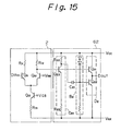
- Figure 15 shows the circuit construction of still another embodiment according to the present invention, in which the output step circuit D2 in the output circuit 62 is constructed without using the resistor R21 and capacitor C22, as in the embodiment shown in Figure 12.
Landscapes
- Engineering & Computer Science (AREA)
- Physics & Mathematics (AREA)
- Computer Hardware Design (AREA)
- Computing Systems (AREA)
- General Engineering & Computer Science (AREA)
- Mathematical Physics (AREA)
- Power Engineering (AREA)
- Logic Circuits (AREA)
Applications Claiming Priority (6)
| Application Number | Priority Date | Filing Date | Title |
|---|---|---|---|
| JP240136/89 | 1989-09-18 | ||
| JP1240136A JPH03102914A (ja) | 1989-09-18 | 1989-09-18 | 出力回路 |
| JP286103/89 | 1989-11-02 | ||
| JP1286103A JPH03147420A (ja) | 1989-11-02 | 1989-11-02 | Ecl論理回路 |
| JP339451/89 | 1989-12-28 | ||
| JP1339451A JPH03201718A (ja) | 1989-12-28 | 1989-12-28 | 出力回路 |
Publications (2)
| Publication Number | Publication Date |
|---|---|
| EP0423940A2 true EP0423940A2 (de) | 1991-04-24 |
| EP0423940A3 EP0423940A3 (en) | 1991-11-13 |
Family
ID=27332782
Family Applications (1)
| Application Number | Title | Priority Date | Filing Date |
|---|---|---|---|
| EP19900310171 Withdrawn EP0423940A3 (en) | 1989-09-18 | 1990-09-18 | A logic circuit |
Country Status (2)
| Country | Link |
|---|---|
| EP (1) | EP0423940A3 (de) |
| KR (1) | KR930009491B1 (de) |
Cited By (12)
| Publication number | Priority date | Publication date | Assignee | Title |
|---|---|---|---|---|
| EP0473352A3 (en) * | 1990-08-22 | 1992-08-05 | Nec Corporation | Emitter follower output circuit |
| EP0511646A1 (de) * | 1991-04-30 | 1992-11-04 | Nec Corporation | Logikschaltung mit hoher Schaltgeschwindigkeit |
| EP0632595A1 (de) * | 1993-06-28 | 1995-01-04 | Siemens Aktiengesellschaft | Leitungstreiberschaltstufe in Stromschaltertechnik |
| DE19730745C2 (de) * | 1996-12-27 | 2002-08-29 | Mitsubishi Electric Eng | Emittergekoppelte Logikschaltung |
| RU2693298C1 (ru) * | 2018-10-16 | 2019-07-02 | Федеральное государственное бюджетное образовательное учреждение высшего образования "Юго-Западный государственный университет" (ЮЗГУ) | Триггерный логический элемент ИЛИ-НЕ на полевых транзисторах |
| RU2710937C1 (ru) * | 2018-10-09 | 2020-01-14 | Федеральное государственное бюджетное образовательное учреждение высшего образования "Юго-Западный государственный университет" (ЮЗГУ) | Триггерный логический элемент ИЛИ-НЕ |
| RU2726853C1 (ru) * | 2020-02-03 | 2020-07-16 | Федеральное государственное бюджетное образовательное учреждение высшего образования. "Юго-Западный государственный университет" (ЮЗГУ) | Триггерный логический элемент ИЛИ/ИЛИ-НЕ |
| RU2760464C1 (ru) * | 2021-04-28 | 2021-11-25 | Федеральное государственное бюджетное образовательное учреждение высшего образования «Юго-Западный государственный университет» | Триггерный логический элемент И-НЕ |
| RU2763152C1 (ru) * | 2021-05-27 | 2021-12-27 | Федеральное государственное бюджетное образовательное учреждение высшего образования «Юго-Западный государственный университет» | Триггерный логический элемент НЕ/ИЛИ/И/ИЛИ-НЕ/И-НЕ на полевых транзисторах |
| RU2763585C1 (ru) * | 2021-05-27 | 2021-12-30 | Федеральное государственное бюджетное образовательное учреждение высшего образования «Юго-Западный государственный университет» (ЮЗГУ) (RU) | Триггерный логический элемент И/И-НЕ на полевых транзисторах |
| RU2767177C1 (ru) * | 2021-06-30 | 2022-03-16 | Федеральное государственное бюджетное образовательное учреждение высшего образования «Юго-Западный государственный университет» (ЮЗГУ) (RU) | Триггерный логический элемент ИЛИ/ИЛИ-НЕ |
| RU2767176C1 (ru) * | 2021-06-30 | 2022-03-16 | Федеральное государственное бюджетное образовательное учреждение высшего образования «Юго-Западный государственный университет» | Триггерный логический элемент ИЛИ-НЕ |
Family Cites Families (4)
| Publication number | Priority date | Publication date | Assignee | Title |
|---|---|---|---|---|
| US3978347A (en) * | 1974-10-02 | 1976-08-31 | Motorola, Inc. | High band width emitter coupled logic gate |
| US4683383A (en) * | 1984-07-19 | 1987-07-28 | Tandem Computers Incorporated | Driver circuit for a three-state gate array using low driving current |
| JPS6177424A (ja) * | 1984-09-25 | 1986-04-21 | Fujitsu Ltd | Ecl回路 |
| US4926065A (en) * | 1987-11-17 | 1990-05-15 | Applied Micro Circuits Corporation | Method and apparatus for coupling an ECL output signal using a clamped capacitive bootstrap circuit |
-
1990
- 1990-09-17 KR KR1019900014677A patent/KR930009491B1/ko not_active Expired - Fee Related
- 1990-09-18 EP EP19900310171 patent/EP0423940A3/en not_active Withdrawn
Cited By (14)
| Publication number | Priority date | Publication date | Assignee | Title |
|---|---|---|---|---|
| US5233234A (en) * | 1990-08-22 | 1993-08-03 | Nec Corporation | Emitter follower output circuit |
| EP0473352A3 (en) * | 1990-08-22 | 1992-08-05 | Nec Corporation | Emitter follower output circuit |
| EP0511646A1 (de) * | 1991-04-30 | 1992-11-04 | Nec Corporation | Logikschaltung mit hoher Schaltgeschwindigkeit |
| US5237216A (en) * | 1991-04-30 | 1993-08-17 | Nec Corporation | High-speed cml push-pull logic circuit having temperature compensated biasing |
| EP0632595A1 (de) * | 1993-06-28 | 1995-01-04 | Siemens Aktiengesellschaft | Leitungstreiberschaltstufe in Stromschaltertechnik |
| DE19730745C2 (de) * | 1996-12-27 | 2002-08-29 | Mitsubishi Electric Eng | Emittergekoppelte Logikschaltung |
| RU2710937C1 (ru) * | 2018-10-09 | 2020-01-14 | Федеральное государственное бюджетное образовательное учреждение высшего образования "Юго-Западный государственный университет" (ЮЗГУ) | Триггерный логический элемент ИЛИ-НЕ |
| RU2693298C1 (ru) * | 2018-10-16 | 2019-07-02 | Федеральное государственное бюджетное образовательное учреждение высшего образования "Юго-Западный государственный университет" (ЮЗГУ) | Триггерный логический элемент ИЛИ-НЕ на полевых транзисторах |
| RU2726853C1 (ru) * | 2020-02-03 | 2020-07-16 | Федеральное государственное бюджетное образовательное учреждение высшего образования. "Юго-Западный государственный университет" (ЮЗГУ) | Триггерный логический элемент ИЛИ/ИЛИ-НЕ |
| RU2760464C1 (ru) * | 2021-04-28 | 2021-11-25 | Федеральное государственное бюджетное образовательное учреждение высшего образования «Юго-Западный государственный университет» | Триггерный логический элемент И-НЕ |
| RU2763152C1 (ru) * | 2021-05-27 | 2021-12-27 | Федеральное государственное бюджетное образовательное учреждение высшего образования «Юго-Западный государственный университет» | Триггерный логический элемент НЕ/ИЛИ/И/ИЛИ-НЕ/И-НЕ на полевых транзисторах |
| RU2763585C1 (ru) * | 2021-05-27 | 2021-12-30 | Федеральное государственное бюджетное образовательное учреждение высшего образования «Юго-Западный государственный университет» (ЮЗГУ) (RU) | Триггерный логический элемент И/И-НЕ на полевых транзисторах |
| RU2767177C1 (ru) * | 2021-06-30 | 2022-03-16 | Федеральное государственное бюджетное образовательное учреждение высшего образования «Юго-Западный государственный университет» (ЮЗГУ) (RU) | Триггерный логический элемент ИЛИ/ИЛИ-НЕ |
| RU2767176C1 (ru) * | 2021-06-30 | 2022-03-16 | Федеральное государственное бюджетное образовательное учреждение высшего образования «Юго-Западный государственный университет» | Триггерный логический элемент ИЛИ-НЕ |
Also Published As
| Publication number | Publication date |
|---|---|
| EP0423940A3 (en) | 1991-11-13 |
| KR930009491B1 (ko) | 1993-10-04 |
| KR910007280A (ko) | 1991-04-30 |
Similar Documents
| Publication | Publication Date | Title |
|---|---|---|
| US5289055A (en) | Digital ECL bipolar logic gates suitable for low-voltage operation | |
| EP0423940A2 (de) | Logische Schaltung | |
| US4804869A (en) | BiMOS logical circuit | |
| US4577125A (en) | Output voltage driver with transient active pull-down | |
| US5089724A (en) | High-speed low-power ECL/NTL circuits with AC-coupled complementary push-pull output stage | |
| EP0219867B1 (de) | Logische Schaltung | |
| US5216296A (en) | Logic circuit having sharper falling edge transition | |
| US5059827A (en) | ECL circuit with low voltage/fast pull-down | |
| EP0183464A2 (de) | Emittergekoppelte logische Schaltungen | |
| JP3530582B2 (ja) | シングルエンド入力論理ゲートを有する集積論理回路 | |
| US4931673A (en) | ECL-to-TTL translator circuit with ground bounce protection | |
| US6255857B1 (en) | Signal level shifting circuits | |
| JPH0777348B2 (ja) | イネーブルゲート | |
| US5101124A (en) | ECL to TTL translator circuit with improved slew rate | |
| JPH07303037A (ja) | エミッタ結合型論理回路 | |
| EP0328842B1 (de) | Halb-Stromschalter mit Rückkopplung | |
| JPH10513031A (ja) | 容量放電結合チャージポンプを用いたアクティブプルダウン回路 | |
| US5789946A (en) | Active pull down emitter coupled logic circuit | |
| JPH071865B2 (ja) | エミッタ結合論理回路 | |
| KR100247313B1 (ko) | 논리 회로 | |
| US4682056A (en) | Switching circuit having low speed/power product | |
| US5508642A (en) | Series-gated emitter-coupled logic circuit providing closely spaced output voltages | |
| US3612913A (en) | Digital circuit | |
| EP0520830A2 (de) | Vorrichtung und Verfahren zur Konversion eines ECL-ähnlichen Signals in einem CMOS-Signal | |
| JP2861356B2 (ja) | 半導体集積回路 |
Legal Events
| Date | Code | Title | Description |
|---|---|---|---|
| PUAI | Public reference made under article 153(3) epc to a published international application that has entered the european phase |
Free format text: ORIGINAL CODE: 0009012 |
|
| AK | Designated contracting states |
Kind code of ref document: A2 Designated state(s): DE FR GB |
|
| PUAL | Search report despatched |
Free format text: ORIGINAL CODE: 0009013 |
|
| AK | Designated contracting states |
Kind code of ref document: A3 Designated state(s): DE FR GB |
|
| 17P | Request for examination filed |
Effective date: 19920108 |
|
| 17Q | First examination report despatched |
Effective date: 19940923 |
|
| STAA | Information on the status of an ep patent application or granted ep patent |
Free format text: STATUS: THE APPLICATION IS DEEMED TO BE WITHDRAWN |
|
| 18D | Application deemed to be withdrawn |
Effective date: 19950204 |