EP0423973B1 - Interconnexions au niveau du gate en silicide - Google Patents
Interconnexions au niveau du gate en silicide Download PDFInfo
- Publication number
- EP0423973B1 EP0423973B1 EP90310818A EP90310818A EP0423973B1 EP 0423973 B1 EP0423973 B1 EP 0423973B1 EP 90310818 A EP90310818 A EP 90310818A EP 90310818 A EP90310818 A EP 90310818A EP 0423973 B1 EP0423973 B1 EP 0423973B1
- Authority
- EP
- European Patent Office
- Prior art keywords
- silicide
- dielectric
- gate material
- recited
- gate
- Prior art date
- Legal status (The legal status is an assumption and is not a legal conclusion. Google has not performed a legal analysis and makes no representation as to the accuracy of the status listed.)
- Expired - Lifetime
Links
Images
Classifications
-
- H—ELECTRICITY
- H10—SEMICONDUCTOR DEVICES; ELECTRIC SOLID-STATE DEVICES NOT OTHERWISE PROVIDED FOR
- H10W—GENERIC PACKAGES, INTERCONNECTIONS, CONNECTORS OR OTHER CONSTRUCTIONAL DETAILS OF DEVICES COVERED BY CLASS H10
- H10W20/00—Interconnections in chips, wafers or substrates
- H10W20/01—Manufacture or treatment
- H10W20/031—Manufacture or treatment of conductive parts of the interconnections
- H10W20/064—Manufacture or treatment of conductive parts of the interconnections by modifying the conductivity of conductive parts, e.g. by alloying
- H10W20/066—Manufacture or treatment of conductive parts of the interconnections by modifying the conductivity of conductive parts, e.g. by alloying by forming silicides of refractory metals
-
- H—ELECTRICITY
- H10—SEMICONDUCTOR DEVICES; ELECTRIC SOLID-STATE DEVICES NOT OTHERWISE PROVIDED FOR
- H10D—INORGANIC ELECTRIC SEMICONDUCTOR DEVICES
- H10D64/00—Electrodes of devices having potential barriers
- H10D64/01—Manufacture or treatment
- H10D64/013—Manufacture or treatment of electrodes having a conductor capacitively coupled to a semiconductor by an insulator
- H10D64/01302—Manufacture or treatment of electrodes having a conductor capacitively coupled to a semiconductor by an insulator the insulator being formed after the semiconductor body, the semiconductor being silicon
- H10D64/01304—Manufacture or treatment of electrodes having a conductor capacitively coupled to a semiconductor by an insulator the insulator being formed after the semiconductor body, the semiconductor being silicon characterised by the conductor
- H10D64/01306—Manufacture or treatment of electrodes having a conductor capacitively coupled to a semiconductor by an insulator the insulator being formed after the semiconductor body, the semiconductor being silicon characterised by the conductor the conductor comprising a layer of silicon contacting the insulator, e.g. polysilicon
- H10D64/01308—Manufacture or treatment of electrodes having a conductor capacitively coupled to a semiconductor by an insulator the insulator being formed after the semiconductor body, the semiconductor being silicon characterised by the conductor the conductor comprising a layer of silicon contacting the insulator, e.g. polysilicon the conductor further comprising a non-elemental silicon additional conductive layer, e.g. a metal silicide layer formed by the reaction of silicon with an implanted metal
- H10D64/0131—Manufacture or treatment of electrodes having a conductor capacitively coupled to a semiconductor by an insulator the insulator being formed after the semiconductor body, the semiconductor being silicon characterised by the conductor the conductor comprising a layer of silicon contacting the insulator, e.g. polysilicon the conductor further comprising a non-elemental silicon additional conductive layer, e.g. a metal silicide layer formed by the reaction of silicon with an implanted metal the additional conductive layer comprising a silicide layer formed by the silicidation reaction between the layer of silicon with a metal layer which is not formed by metal implantation
-
- H—ELECTRICITY
- H10—SEMICONDUCTOR DEVICES; ELECTRIC SOLID-STATE DEVICES NOT OTHERWISE PROVIDED FOR
- H10D—INORGANIC ELECTRIC SEMICONDUCTOR DEVICES
- H10D64/00—Electrodes of devices having potential barriers
- H10D64/01—Manufacture or treatment
- H10D64/013—Manufacture or treatment of electrodes having a conductor capacitively coupled to a semiconductor by an insulator
- H10D64/01302—Manufacture or treatment of electrodes having a conductor capacitively coupled to a semiconductor by an insulator the insulator being formed after the semiconductor body, the semiconductor being silicon
- H10D64/01304—Manufacture or treatment of electrodes having a conductor capacitively coupled to a semiconductor by an insulator the insulator being formed after the semiconductor body, the semiconductor being silicon characterised by the conductor
- H10D64/01326—Aspects related to lithography, isolation or planarisation of the conductor
Definitions
- This invention relates to integrated circuits using silicide interconnections between components.
- Integrated circuits require low resistance electrical contacts to components, as well as low resistance interconnects or runners between components.
- polysilicon has a relatively low resistivity and has been widely and successfully used for both applications, alternative materials have been sought in an attempt to obtain even lower resistivities. As the dimensions of components continue to decrease, such lower resistivity alternatives become even more desirable because the resistance of the interconnect is inversely proportional to its cross-sectional area.
- the most commonly used alternative to polysilicon is a transition metal silicide.
- fabrication of a silicide proceeds by depositing the transition metal, such as Ti or Co, on silicon and heating the resulting composite. The transition metal reacts with the silicon to form the silicide.
- the silicon is present only where the silicide is ultimately desired and there is no need to remove unwanted silicide, although the unreacted metal must be removed by, e.g., etching.
- the resulting silicide is self-aligned and is frequently referred to by those skilled in the art as salicide ( s elf- a capitad sili cide ).
- Salicides are used on gate electrodes, source/drain region electrical contacts, and interconnects.
- Another exemplary technique fabricates structures that are called polycides. Polysilicon and transition metal silicide layers are sequentially deposited and then simultaneously patterned. Both the gate and gate runner have a silicide on top. However, the gate etching may be difficult to control due to the silicide/polysilicon structure.
- the chemical reaction between silicon and the metal necessarily consumes some of the underlying silicon; i.e., the underlying silicon reacts with the metal to form the silicide.
- deposition of a thick metal layer, necessary to obtain a thick, low-resistance, silicide layer, is frequently undesirable on both the gate and the source/drain regions.
- a thick silicide layer in the gate may produce either a high stress which adversely affects the quality of both the gate oxide and the device characteristics, or some silicide which penetrates the gate oxide and also adversely affect the device characteristics. The likelihood of the latter problem becomes greater as gate oxides continue to become thinner.
- Silicides are desirable on the source/drain regions because they have low resistance as compared to other materials. However, the source/drain regions should be shallow in integrated circuit devices having submicron features, and a thick metal deposition on these regions might lead to a reaction that would consume all, or a substantial fraction, of these regions.
- silicide containing structure for both the source/drain regions and the runners is theoretically possible, but is difficult to implement in practice because of the conflicting requirements of a thick silicide on the runners and a thin silicide on the source and drain regions.
- materials other than polysilicon and silicides in the gate and for interconnects there exist similar considerations to the use of materials other than polysilicon and silicides in the gate and for interconnects.
- EP-A-0285410 discloses a method for forming vertical metal interconnects on a semiconductor substrate having an uneven surface which comprises first forming a laminated metal structure over the entire substrate.
- the laminated metal structure includes a first metallization sublayer, an intermediate etch stop barrier layer, and a second metallization sublayer.
- the laminated metal structure is then patterned into the desired vertical metal interconnects, which interconnects are at different elevations because of the uneven underlying surface.
- the vertical metal interconnects are then planarized by first applying a dielectric layer and a sacrificial layer, etching back the combined dielectric and sacrificial layers to expose only the higher vertical metal interconnects, and then selectively etching back the second metal sublayer component of the higher vertical metal interconnects.
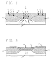
- FIGS. 1 and 2 are sectional views of structures useful in explaining the method of this invention. For reasons of clarity, the elements depicted are not drawn to scale.
- FIG. 1 is a sectional view of a portion of an integrated circuit, i.e., a field-effect transistor, at an intermediate stage of fabrication according to this invention. Depicted are substrate 1; gate structure 3, which has insulating sidewalls 5, polysilicon conductor 7, and, optionally, dielectric layer 9 on top of the polysilicon; source/drain regions 11, field oxide 13, second dielectric layer 15; and polysilicon runners 17 on the field oxide.
- the area between the field oxide regions, which contains the gate structure and the source/drain regions, is termed a device region.
- Silicide layers 19 contact the source/drain regions 11.
- the runners also have insulating sidewalls 5.
- An integrated circuit will have many transistors; only a portion of a single transistor is depicted for clarity of exposition.
- the elements depicted are fabricated using well-known techniques which need not be described in detail, as the techniques are known to those skilled in the art. Some device elements, such as the gate oxide, are not depicted as they are not essential to the description of device fabrication. Several features of an exemplary fabrication sequence will, however, be briefly noted.
- the polysilicon is blanket deposited and lithographically patterned to form the runners 17 and gate structure 7.
- a salicidation step can be performed to fabricate the thin salicide regions 19. If the gate structure does not have a dielectric on top of the polysilicon, a salicide may be formed on top of the gate structure.
- An etchback planarizes the first dielectric and leaves the top surfaces of the polysilicon runners 17 exposed. If a dielectric is initially present on top of the runners, it is removed by the planarization etch, as shown in FIG. 1. Etching is stopped as soon as the surfaces of the runners are cleared of dielectric material so that the device elements; i.e., source/drain regions and gate structure, are not exposed. Some over-etching is desirable to ensure that the top surfaces of all runners are clear.
- a silicide-forming transition metal such as Ti or Co, is now blanket deposited and the structure heated to form a silicide on the exposed portions of the runners, which are, as previously mentioned, primarily the top surface of the runner.
- the thickness of the deposited metal is determined by the desired thickness of the silicide. Unreacted metal is removed and another, i.e., second, dielectric layer is deposited to the final desired thickness. The second dielectric layer is then patterned to form windows for the electrical contacts to the device elements; i.e., source, drain, and gate.
- FIG. 2 is a sectional view at right angles to that of FIG. 1. Depicted are substrate 1, layer 9, field oxide regions 13, dielectric layer 15, patterned polysilicon layer 17; and device region 23, which is between the field oxide regions. Within device region 23 are the gate and source/drain regions; these elements are not depicted for reasons of clarity. The fabrication technique is that described with respect to FIG. 1.
- the dielectric layer 15 is generally thicker in the device region 23 than it is on the field oxide region 13 due to the presence of the field oxide.
- the planarizing etchback clears patterned polysilicon 17 on the field oxide regions but will not affect any of the device elements, including the gate, which are masked by dielectric 15.
- Layer 9 may be, e.g., a salicide or a dielectric.
- the source/drain regions need not be salicide regions 19, as the salicidation step for these regions may be omitted, if desired. If they are salicide regions, the dielectric on top of the gate structure is omitted if gate salicidation is desired. The salicide so formed will be thin. The presence of the dielectric on the gate structure prevents silicide formation on the polysilicon if gate salicidation is undesired.
- the described process leads to thin silicides for the source/drain regions and a thick silicide for the runners. Additionally, it will be readily appreciated that the second dielectric layer will have an essentially planar surface which may be used for patterned metallizations.
- the conducting gate material might comprise a conducting nitride, such as TiN.
- the conductivity of the exposed conducting gate material i.e., runner, might be increased by selective deposition of a metal such as tungsten.
Landscapes
- Electrodes Of Semiconductors (AREA)
- Insulated Gate Type Field-Effect Transistor (AREA)
- Internal Circuitry In Semiconductor Integrated Circuit Devices (AREA)
Claims (6)
- Procédé de fabrication de circuits intégrés comprenant les étapes :de dépôt d'une couche de matière de grille conductrice (17) sur un substrat (1) qui comporte des zones d'oxyde de champ (13) et des zones de dispositif composant une structure de grille (3) ;d'application d'un motif sur ladite matière de grille conductrice (17) sur lesdites zones d'oxyde de champ (13) ;de formation d'un premier diélectrique (15) par-dessus ledit substrat (1) qui recouvre la matière de grille (17) ;d'élimination par gravure dudit diélectrique (15) en vue d'exposer les surfaces supérieures de ladite matière de grille conductrice (17) sur lesdites zones d'oxyde de champ (13) mais non sur lesdites zones de dispositif ; etd'augmentation de la conductivité de ladite matière de grille conductrice exposée (17).
- Procédé selon la revendication 1, dans lequel ladite matière de grille conductrice (17) comprend du polysicilium.
- Procédé selon la revendication 2, dans lequel ladite étape d'augmentation comprend les étapes :de dépôt d'un métal de transition formant un siliciure ; etde chauffage en vue de former un siliciure.
- Procédé selon la revendication 1, comprenant l'autre étape de dépôt et d'application d'un motif sur un deuxième diélectrique en vue de former des fenêtres qui exposent des parties sélectionnées desdites zones de dispositif.
- Procédé selon la revendication 4, comprenant l'autre étape de dépôt d'un métal dans lesdites fenêtres.
- Procédé selon la revendication 1, dans lequel ladite étape d'augmentation comprend le dépôt de tungstène sélectivement sur lesdits rails conducteurs exposés.
Applications Claiming Priority (2)
| Application Number | Priority Date | Filing Date | Title |
|---|---|---|---|
| US07/420,207 US4935376A (en) | 1989-10-12 | 1989-10-12 | Making silicide gate level runners |
| US420207 | 1989-10-12 |
Publications (3)
| Publication Number | Publication Date |
|---|---|
| EP0423973A2 EP0423973A2 (fr) | 1991-04-24 |
| EP0423973A3 EP0423973A3 (en) | 1992-09-23 |
| EP0423973B1 true EP0423973B1 (fr) | 2001-06-13 |
Family
ID=23665519
Family Applications (1)
| Application Number | Title | Priority Date | Filing Date |
|---|---|---|---|
| EP90310818A Expired - Lifetime EP0423973B1 (fr) | 1989-10-12 | 1990-10-03 | Interconnexions au niveau du gate en silicide |
Country Status (4)
| Country | Link |
|---|---|
| US (1) | US4935376A (fr) |
| EP (1) | EP0423973B1 (fr) |
| JP (1) | JP3039798B2 (fr) |
| DE (1) | DE69033747T2 (fr) |
Families Citing this family (7)
| Publication number | Priority date | Publication date | Assignee | Title |
|---|---|---|---|---|
| US5461005A (en) * | 1991-12-27 | 1995-10-24 | At&T Ipm Corp. | Method of forming silicide in integrated circuit manufacture |
| US5654570A (en) * | 1995-04-19 | 1997-08-05 | International Business Machines Corporation | CMOS gate stack |
| US6194296B1 (en) * | 1995-10-31 | 2001-02-27 | Integrated Device Technology, Inc. | Method for making planarized polycide |
| US6074921A (en) * | 1997-06-30 | 2000-06-13 | Vlsi Technology, Inc. | Self-aligned processing of semiconductor device features |
| US6207543B1 (en) | 1997-06-30 | 2001-03-27 | Vlsi Technology, Inc. | Metallization technique for gate electrodes and local interconnects |
| US5953612A (en) * | 1997-06-30 | 1999-09-14 | Vlsi Technology, Inc. | Self-aligned silicidation technique to independently form silicides of different thickness on a semiconductor device |
| US6001721A (en) * | 1998-02-19 | 1999-12-14 | Taiwan Semiconductor Manufacturing Company, Ltd. | Silicide and salicide on the same chip |
Family Cites Families (16)
| Publication number | Priority date | Publication date | Assignee | Title |
|---|---|---|---|---|
| US4455737A (en) * | 1978-05-26 | 1984-06-26 | Rockwell International Corporation | Process for and structure of high density VLSI circuits, having self-aligned gates and contacts for FET devices and conducting lines |
| JPS55125651A (en) * | 1979-03-22 | 1980-09-27 | Nec Corp | Production of semiconductor integrated circuit |
| US4392150A (en) * | 1980-10-27 | 1983-07-05 | National Semiconductor Corporation | MOS Integrated circuit having refractory metal or metal silicide interconnect layer |
| US4382827A (en) * | 1981-04-27 | 1983-05-10 | Ncr Corporation | Silicon nitride S/D ion implant mask in CMOS device fabrication |
| US4374700A (en) * | 1981-05-29 | 1983-02-22 | Texas Instruments Incorporated | Method of manufacturing silicide contacts for CMOS devices |
| JPS57208169A (en) * | 1981-06-17 | 1982-12-21 | Toshiba Corp | Semiconductor device and manufacture thereof |
| JPS5852850A (ja) * | 1981-09-24 | 1983-03-29 | Nec Corp | 半導体装置の製造方法 |
| JPS58130554A (ja) * | 1982-01-28 | 1983-08-04 | Toshiba Corp | 半導体装置の製造方法 |
| US4442591A (en) * | 1982-02-01 | 1984-04-17 | Texas Instruments Incorporated | High-voltage CMOS process |
| JPS6065545A (ja) * | 1983-09-21 | 1985-04-15 | Hitachi Micro Comput Eng Ltd | 半導体装置の製造方法 |
| FR2555364B1 (fr) * | 1983-11-18 | 1990-02-02 | Hitachi Ltd | Procede de fabrication de connexions d'un dispositif a circuits integres a semi-conducteurs comportant en particulier un mitset |
| KR940006668B1 (ko) * | 1984-11-22 | 1994-07-25 | 가부시끼가이샤 히다찌세이사꾸쇼 | 반도체 집적회로 장치의 제조방법 |
| US4619038A (en) * | 1985-08-15 | 1986-10-28 | Motorola, Inc. | Selective titanium silicide formation |
| JPS63133551A (ja) * | 1986-11-26 | 1988-06-06 | Agency Of Ind Science & Technol | 半導体装置の製造方法 |
| US4824521A (en) * | 1987-04-01 | 1989-04-25 | Fairchild Semiconductor Corporation | Planarization of metal pillars on uneven substrates |
| US4822749A (en) * | 1987-08-27 | 1989-04-18 | North American Philips Corporation, Signetics Division | Self-aligned metallization for semiconductor device and process using selectively deposited tungsten |
-
1989
- 1989-10-12 US US07/420,207 patent/US4935376A/en not_active Expired - Lifetime
-
1990
- 1990-10-03 EP EP90310818A patent/EP0423973B1/fr not_active Expired - Lifetime
- 1990-10-03 DE DE69033747T patent/DE69033747T2/de not_active Expired - Lifetime
- 1990-10-12 JP JP2272492A patent/JP3039798B2/ja not_active Expired - Lifetime
Non-Patent Citations (1)
| Title |
|---|
| Journal Vacuum Sci.& Technology, vol.17, No.4, pages 775-792, 1980,by S.P. Muraka et al. * |
Also Published As
| Publication number | Publication date |
|---|---|
| US4935376A (en) | 1990-06-19 |
| JPH03138929A (ja) | 1991-06-13 |
| DE69033747D1 (de) | 2001-07-19 |
| DE69033747T2 (de) | 2002-02-28 |
| EP0423973A2 (fr) | 1991-04-24 |
| JP3039798B2 (ja) | 2000-05-08 |
| EP0423973A3 (en) | 1992-09-23 |
Similar Documents
| Publication | Publication Date | Title |
|---|---|---|
| KR100187870B1 (ko) | 반도체 구조물 및 그 제조 방법 | |
| US5464782A (en) | Method to ensure isolation between source-drain and gate electrode using self aligned silicidation | |
| EP0497595B1 (fr) | Interconnexion locale pour circuits intégrés | |
| US4392150A (en) | MOS Integrated circuit having refractory metal or metal silicide interconnect layer | |
| US5610099A (en) | Process for fabricating transistors using composite nitride structure | |
| EP0517368B1 (fr) | Interconnexion locale pour circuits intégrés | |
| US5200358A (en) | Integrated circuit with planar dielectric layer | |
| US4822749A (en) | Self-aligned metallization for semiconductor device and process using selectively deposited tungsten | |
| EP0540446B1 (fr) | Piliers de contact autoalignés pour dispositifs semi-conducteurs | |
| US6004878A (en) | Method for silicide stringer removal in the fabrication of semiconductor integrated circuits | |
| US4933297A (en) | Method for etching windows having different depths | |
| GB2077993A (en) | Low sheet resistivity composite conductor gate MOS device | |
| JP2697797B2 (ja) | 金属・ポリシリコン二重層ゲートの形成方法 | |
| EP0603360A1 (fr) | Procedes de formation d'une interconnexion locale et d'une charge de polysilicium a resistance elevee | |
| US5989987A (en) | Method of forming a self-aligned contact in semiconductor fabrications | |
| US4935376A (en) | Making silicide gate level runners | |
| EP0526244B1 (fr) | Procédé de formation d'un contact enterré en silicium polycristallin | |
| JP2001237427A (ja) | 拡張されたソース/ドレインコンタクト領域を有する隆起シリサイドソース/ドレイン型mosトランジスタおよび方法 | |
| KR100275739B1 (ko) | 역방향 자기정합 구조의 트랜지스터 및 그 제조방법 | |
| US6066532A (en) | Method of fabricating embedded gate electrodes | |
| US6483153B1 (en) | Method to improve LDD corner control with an in-situ film for local interconnect processing | |
| US6136698A (en) | Method of increasing contact area of a contact window | |
| US6096643A (en) | Method of fabricating a semiconductor device having polysilicon line with extended silicide layer | |
| US6096639A (en) | Method of forming a local interconnect by conductive layer patterning | |
| US6165882A (en) | Polysilicon gate having a metal plug, for reduced gate resistance, within a trench extending into the polysilicon layer of the gate |
Legal Events
| Date | Code | Title | Description |
|---|---|---|---|
| PUAI | Public reference made under article 153(3) epc to a published international application that has entered the european phase |
Free format text: ORIGINAL CODE: 0009012 |
|
| AK | Designated contracting states |
Kind code of ref document: A2 Designated state(s): DE FR GB IT |
|
| PUAL | Search report despatched |
Free format text: ORIGINAL CODE: 0009013 |
|
| AK | Designated contracting states |
Kind code of ref document: A3 Designated state(s): DE FR GB IT |
|
| 17P | Request for examination filed |
Effective date: 19930311 |
|
| RAP3 | Party data changed (applicant data changed or rights of an application transferred) |
Owner name: AT&T CORP. |
|
| 17Q | First examination report despatched |
Effective date: 19940714 |
|
| APAA | Appeal reference recorded |
Free format text: ORIGINAL CODE: EPIDOS REFN |
|
| APAD | Appeal reference recorded |
Free format text: ORIGINAL CODE: EPIDOS REFNE |
|
| APCB | Communication from the board of appeal sent |
Free format text: ORIGINAL CODE: EPIDOS OBAPE |
|
| APCB | Communication from the board of appeal sent |
Free format text: ORIGINAL CODE: EPIDOS OBAPE |
|
| APAB | Appeal dossier modified |
Free format text: ORIGINAL CODE: EPIDOS NOAPE |
|
| GRAG | Despatch of communication of intention to grant |
Free format text: ORIGINAL CODE: EPIDOS AGRA |
|
| GRAH | Despatch of communication of intention to grant a patent |
Free format text: ORIGINAL CODE: EPIDOS IGRA |
|
| RIC1 | Information provided on ipc code assigned before grant |
Free format text: 7H 01L 21/768 A, 7H 01L 21/28 B |
|
| GRAH | Despatch of communication of intention to grant a patent |
Free format text: ORIGINAL CODE: EPIDOS IGRA |
|
| GRAA | (expected) grant |
Free format text: ORIGINAL CODE: 0009210 |
|
| AK | Designated contracting states |
Kind code of ref document: B1 Designated state(s): DE FR GB IT |
|
| REF | Corresponds to: |
Ref document number: 69033747 Country of ref document: DE Date of ref document: 20010719 |
|
| ITF | It: translation for a ep patent filed | ||
| ET | Fr: translation filed | ||
| REG | Reference to a national code |
Ref country code: GB Ref legal event code: IF02 |
|
| PLBE | No opposition filed within time limit |
Free format text: ORIGINAL CODE: 0009261 |
|
| STAA | Information on the status of an ep patent application or granted ep patent |
Free format text: STATUS: NO OPPOSITION FILED WITHIN TIME LIMIT |
|
| 26N | No opposition filed | ||
| PG25 | Lapsed in a contracting state [announced via postgrant information from national office to epo] |
Ref country code: IT Free format text: LAPSE BECAUSE OF NON-PAYMENT OF DUE FEES;WARNING: LAPSES OF ITALIAN PATENTS WITH EFFECTIVE DATE BEFORE 2007 MAY HAVE OCCURRED AT ANY TIME BEFORE 2007. THE CORRECT EFFECTIVE DATE MAY BE DIFFERENT FROM THE ONE RECORDED. Effective date: 20051003 |
|
| APAH | Appeal reference modified |
Free format text: ORIGINAL CODE: EPIDOSCREFNO |
|
| PGFP | Annual fee paid to national office [announced via postgrant information from national office to epo] |
Ref country code: DE Payment date: 20091026 Year of fee payment: 20 |
|
| PGFP | Annual fee paid to national office [announced via postgrant information from national office to epo] |
Ref country code: GB Payment date: 20091022 Year of fee payment: 20 Ref country code: FR Payment date: 20091110 Year of fee payment: 20 |
|
| REG | Reference to a national code |
Ref country code: GB Ref legal event code: PE20 Expiry date: 20101002 |
|
| PG25 | Lapsed in a contracting state [announced via postgrant information from national office to epo] |
Ref country code: GB Free format text: LAPSE BECAUSE OF EXPIRATION OF PROTECTION Effective date: 20101002 |
|
| PG25 | Lapsed in a contracting state [announced via postgrant information from national office to epo] |
Ref country code: DE Free format text: LAPSE BECAUSE OF EXPIRATION OF PROTECTION Effective date: 20101003 |