EP0424018A2 - Verfahren zum Isolieren mit Feldoxyd für integrierte Schaltungen - Google Patents
Verfahren zum Isolieren mit Feldoxyd für integrierte Schaltungen Download PDFInfo
- Publication number
- EP0424018A2 EP0424018A2 EP90311086A EP90311086A EP0424018A2 EP 0424018 A2 EP0424018 A2 EP 0424018A2 EP 90311086 A EP90311086 A EP 90311086A EP 90311086 A EP90311086 A EP 90311086A EP 0424018 A2 EP0424018 A2 EP 0424018A2
- Authority
- EP
- European Patent Office
- Prior art keywords
- oxide
- layer
- spacer
- substrate
- field oxide
- Prior art date
- Legal status (The legal status is an assumption and is not a legal conclusion. Google has not performed a legal analysis and makes no representation as to the accuracy of the status listed.)
- Withdrawn
Links
Images


Classifications
-
- H—ELECTRICITY
- H10—SEMICONDUCTOR DEVICES; ELECTRIC SOLID-STATE DEVICES NOT OTHERWISE PROVIDED FOR
- H10P—GENERIC PROCESSES OR APPARATUS FOR THE MANUFACTURE OR TREATMENT OF DEVICES COVERED BY CLASS H10
- H10P14/00—Formation of materials, e.g. in the shape of layers or pillars
- H10P14/60—Formation of materials, e.g. in the shape of layers or pillars of insulating materials
- H10P14/61—Formation of materials, e.g. in the shape of layers or pillars of insulating materials using masks
-
- H—ELECTRICITY
- H10—SEMICONDUCTOR DEVICES; ELECTRIC SOLID-STATE DEVICES NOT OTHERWISE PROVIDED FOR
- H10W—GENERIC PACKAGES, INTERCONNECTIONS, CONNECTORS OR OTHER CONSTRUCTIONAL DETAILS OF DEVICES COVERED BY CLASS H10
- H10W10/00—Isolation regions in semiconductor bodies between components of integrated devices
- H10W10/01—Manufacture or treatment
- H10W10/011—Manufacture or treatment of isolation regions comprising dielectric materials
- H10W10/012—Manufacture or treatment of isolation regions comprising dielectric materials using local oxidation of silicon [LOCOS]
-
- H—ELECTRICITY
- H10—SEMICONDUCTOR DEVICES; ELECTRIC SOLID-STATE DEVICES NOT OTHERWISE PROVIDED FOR
- H10W—GENERIC PACKAGES, INTERCONNECTIONS, CONNECTORS OR OTHER CONSTRUCTIONAL DETAILS OF DEVICES COVERED BY CLASS H10
- H10W10/00—Isolation regions in semiconductor bodies between components of integrated devices
- H10W10/10—Isolation regions comprising dielectric materials
- H10W10/13—Isolation regions comprising dielectric materials formed using local oxidation of silicon [LOCOS], e.g. sealed interface localised oxidation [SILO] or side-wall mask isolation [SWAMI]
Definitions
- This invention relates to semiconductor devices and methods for manufacturing them; more particularly, it relates to methods for fabricating interdevice isolation structures on a semiconductor chip.
- LOCOS Local Oxidation of Silicon
- the LOCOS process involves the formation of a silicon dioxide pad layer upon a bare silicon surface. The pad layer is then covered with silicon nitride. Both the pad layer and the silicon nitride layer are then patterned to expose portions of bare silicon. The bare silicon is subsequently oxidized to produce an isolation structure often termed a "field oxide.”
- the thermal oxidation process used to grow the field oxide causes a lifting of the edges of the silicon nitride layer.
- the tapered portion of the field oxide which extends beneath the edge of the silicon nitride layer is often termed a "bird's beak.”
- the presence of the bird's beak effectively increases the size of the field oxide, thereby ultimately decreasing the amount of silicon real estate available for later device formation.
- the final size of the field oxide is generally larger than the original lithographic pattern imposed upon the silicon nitride layer.
- poly buffered LOCOS a layer of polysilicon is formed between the pad oxide and the silicon nitride overlayer.
- the silicon nitride overlayer may be comparatively thick.
- the polysilicon layer being somewhat more forgiving than the comparatively rigid silicon nitride overlayer, serves to absorb stresses generated during the thermal oxidation step. Consequently, the possibility of dislocation formation during the thermal oxidation step is reduced.
- practical experience with the poly buffered LOCOS has still shown an undesirable amount of bird's beak formation - perhaps, because the polysilicon layer compresses slightly, permitting undesirable outward growth of the silicon dioxide.
- a disadvantage to the use of a polysilicon buffer layer is that it tends to permit formation of the feature (i.e., bird's beak) which the overlying thick silicon nitride layer is designed to suppress.
- the present invention provides a method of field oxide formation with greatly reduced bird's beak formation and little risk of damage to the underlying substrate.
- a polysilicon layer is sandwiched between a pad oxide layer and a silicon nitride layer during the initial steps of wafer processing.
- the sandwich is patterned to expose bare silicon at the locations where a field oxide is desired.
- a wet clean is performed to remove a small portion of the pad oxide underneath the polysilicon layer.
- a silicon nitride layer is deposited and anisotropically etched back to form a spacer.
- the spacer has a protruding foot which extends into the region where the pad oxide was removed by the previous wet cleaning step.
- a field oxide is formed. The forming process causes a slight lifting - but very little distortion of - the silicon nitride structure. However, bird's beak formation is minimal (and may be further reduced by subsequent etching).
- the polysilicon layer may be eliminated.
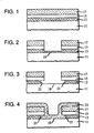
- reference numeral 11 denotes a substrate which typically consists essentially of silicon or epitaxial silicon.
- Pad oxide 13 may be formed by conventional processes upon substrate 11.
- a typical thickness for pad oxide 13 is between 100 ⁇ and 300 ⁇ .
- Polysilicon layer 15 may be formed upon pad oxide 13 by conventional processes.
- a typical thickness for polysilicon layer 15 is between 400 ⁇ and 600 ⁇ .
- Silicon nitride layer 17 is formed upon polysilicon layer 15 by conventional processes.
- a typical thickness for silicon nitride layer 17 is between 1500 ⁇ and 2800 ⁇ . It is possible to eliminate polysilicon layer 15. However, if layer 15 is eliminated, the thickness of layer 17 should be reduced to the approximate range of 800 ⁇ to 1300 ⁇ to avoid stress problems.
- FIG. 2 depicts the structure of FIG. 1 after layers 13, 15 and 17 have been patterned to create opening 19.
- the patterning may be accomplished by those skilled in the art. Usually a photoresist is deposited and portions selectively removed to create an opening in the photoresist. Then layers 17,15, and 13 may be etched through the opening.) It is desired to form a field oxide within opening 19.
- a wet cleaning procedure is performed on the structure illustrated in FIG. 2. As illustrated in FIG. 3, the wet cleaning procedure tends to preferentially attack pad oxide 13, creating gap 21 beneath layer 15.
- a typical solution for performing the wet clean is 15:1 HF solution for approximately 1-2 minutes.
- Gap 21 desirably extends inward about 200-400 ⁇ .
- silicon nitride layer 23 is blanket deposited (typically by one of various chemical vapor deposition techniques known to those skilled in the art) over the structure of FIG. 3. It will be noted that layer 23 protrudes into gap 21.
- layer 23 has been anisotropically etched to produce spacer 25 with foot-like protrusions 27.
- a typical suitable anisotropic etch process involves the use of trifluoromethane and oxygen in a ratio of 45:8 respectively. It will be noted that protrusions 27 extend away from opening 19 within which the field oxide is to be formed.
- field oxide 29 may be formed by high pressure oxidation at 20-25 atm. at approximately 920°C for 15 minutes.
- other processes such as steam thermal oxidation at approximately 950°C-1000°C for approximately one hour may be used.
- field oxides 29 Although the formation of field oxides 29 causes some uplifting of spacer 25 together with foot-like protrusion 27, undesirable bird's beak formation is significantly reduced. It is believed that foot-like protrusions prevent migration of oxygen into layers 13 and 15 while simultaneously helping to prevent excessive lifting of the stack of layers 13,15, and 17 during formation of the field oxide.
- the bird's beak region 31 of field oxide 29 is substantially smaller than the bird's beak produced by, for example, a conventional LOCOS process.
- FIG. 11 illustrates field oxide 29 after an isotropic etch has been performed.
- the size of the field oxide before the isotropic etch is shown in phantom and designated by reference numeral 29′.
- the shape of field oxide 29 is comparatively symmetric about the outer surface 45 of substrate 11, i.e., the size and shape of upper portion 41 of field oxide is similar to the size and shape of lower portion 43.
- field oxides formed from conventional poly buffered LOCOS processes tend to exhibit a disproportionate amount of oxide above the outer surface of the substrate (where it serves no useful purpose).
- FIGs. 7-10 illustrate an alternative process for forming a field oxide according to the present invention.
- the structure depicted in FIG. 7 is formed after the steps depicted by FIGs. 1-3 have been completed.
- additional thin thermal oxide layers 51 and 53 are regrown (preferably in dry oxygen at approximately 850-900°C for approximately 40 minutes).
- the thickness of layers 51 and 53 is approximately 100 ⁇ .
- Layers 51 and 53 provide additional protection against the creation of defects in substrate 11. It will be noted that layer 51 is formed upon substrate 11 in opening 19, while layer 53 grows on the underside of polysilicon layer 15.
- FIG. 8-10 silicon nitride layer 23 is deposited on the structure depicted in FIG. 7.
- spacers 25 are formed by anisotropic etching.
- field oxide 29 is formed by conventional techniques such as those described previously. Finally, layers 13,15,17, and 53 together with spacers 25 are removed, leaving a structure similar to that depicted in FIG. 11. As mentioned before, an isotropic etch may be applied to further reduce the size of the resulting bird's beak.
- polysilicon layer 15 may be omitted. If layer 15 is omitted, of course, the processing sequence is simplified. However, as mentioned before, without a stress relief layer, it is desirable to make the overlying silicon nitride layer 17 somewhat thinner to avoid generation of defects. Because layer 17 is thinner, the bird's beak is not as effectively suppressed, and a slightly larger bird's beak occurs when polysilicon layer 15 is omitted.
- the inventive process provides a variety of advantages over other isolation techniques.
- One advantage of the inventive process is that the size of the field oxide body is smaller than the smallest opening achievable by straightforward lithography.
- Spacer 25 effectively reduces the size of opening 19 and thus permits formation of a smaller field oxide than otherwise possible.
- the spacer also helps to prevent oxygen intrusion into layers 13 and 15.
- the inventive process is expected to generate less silicon defects than the aforementioned Ghezzo et al. process because there is no tilting or bending distortion of the nitride spacer as exhibited in Ghezzo et al.
- the addition of a polysilicon layer between spacers in Ghezzo et al. will not alleviate the defect generation problem.
- the present invention does not exhibit bending or tilting of nitride spacer 25.
- the entire stack of layers 13,17 (and 15 if present) tilts somewhat gradually, thus lessening the likelihood of defect formation.
- the inward foot-like protrusions of applicants' spacer permit a slight raising of the nitride overlayer.
- the outward protrusions of the Ghezzo et al. structure tend to drag the upper surface of the silicon as they tilt, thus contributing to defect formation.
Landscapes
- Local Oxidation Of Silicon (AREA)
- Element Separation (AREA)
Applications Claiming Priority (2)
| Application Number | Priority Date | Filing Date | Title |
|---|---|---|---|
| US42284489A | 1989-10-17 | 1989-10-17 | |
| US422844 | 1999-10-21 |
Publications (2)
| Publication Number | Publication Date |
|---|---|
| EP0424018A2 true EP0424018A2 (de) | 1991-04-24 |
| EP0424018A3 EP0424018A3 (en) | 1991-07-31 |
Family
ID=23676656
Family Applications (1)
| Application Number | Title | Priority Date | Filing Date |
|---|---|---|---|
| EP19900311086 Withdrawn EP0424018A3 (en) | 1989-10-17 | 1990-10-10 | Integrated circuit field isolation process |
Country Status (2)
| Country | Link |
|---|---|
| EP (1) | EP0424018A3 (de) |
| JP (1) | JPH03145131A (de) |
Cited By (8)
| Publication number | Priority date | Publication date | Assignee | Title |
|---|---|---|---|---|
| EP0518418A1 (de) * | 1991-06-10 | 1992-12-16 | Koninklijke Philips Electronics N.V. | Verfahren zum Herstellen einer Halbleiteranordnung, wobei in einer Oberfläche eines Siliziumkörpers durch Oxidation Feldoxidgebiete gebildet werden |
| EP0540149A1 (de) * | 1991-08-30 | 1993-05-05 | STMicroelectronics, Inc. | Verfahren zur Herstellung von isolierenden Gebieten am Oxyd |
| EP0540157A1 (de) * | 1991-09-30 | 1993-05-05 | STMicroelectronics, Inc. | Verfahren zur Herstellung einer submikronen Isolierung für CMOS-Bauelemente |
| US5358893A (en) * | 1993-06-10 | 1994-10-25 | Samsung Electronics Co., Ltd. | Isolation method for semiconductor device |
| US5374584A (en) * | 1992-07-10 | 1994-12-20 | Goldstar Electron Co. Ltd. | Method for isolating elements in a semiconductor chip |
| US5422300A (en) * | 1992-12-03 | 1995-06-06 | Motorola Inc. | Method for forming electrical isolation in an integrated circuit |
| US5977607A (en) * | 1994-09-12 | 1999-11-02 | Stmicroelectronics, Inc. | Method of forming isolated regions of oxide |
| CN117790290A (zh) * | 2024-02-23 | 2024-03-29 | 合肥晶合集成电路股份有限公司 | 半导体结构及其制作方法 |
Families Citing this family (2)
| Publication number | Priority date | Publication date | Assignee | Title |
|---|---|---|---|---|
| KR100419877B1 (ko) * | 1997-06-30 | 2004-06-30 | 주식회사 하이닉스반도체 | 반도체 장치의 소자 분리 방법 |
| JP7645729B2 (ja) * | 2021-07-06 | 2025-03-14 | エイブリック株式会社 | 半導体装置の製造方法 |
Family Cites Families (1)
| Publication number | Priority date | Publication date | Assignee | Title |
|---|---|---|---|---|
| NL8601415A (nl) * | 1986-06-02 | 1988-01-04 | Philips Nv | Werkwijze ter vervaardiging van een halfgeleiderinrichting. |
-
1990
- 1990-10-10 EP EP19900311086 patent/EP0424018A3/en not_active Withdrawn
- 1990-10-17 JP JP2276567A patent/JPH03145131A/ja active Pending
Cited By (10)
| Publication number | Priority date | Publication date | Assignee | Title |
|---|---|---|---|---|
| EP0518418A1 (de) * | 1991-06-10 | 1992-12-16 | Koninklijke Philips Electronics N.V. | Verfahren zum Herstellen einer Halbleiteranordnung, wobei in einer Oberfläche eines Siliziumkörpers durch Oxidation Feldoxidgebiete gebildet werden |
| US5254494A (en) * | 1991-06-10 | 1993-10-19 | U.S. Philips Corp. | Method of manufacturing a semiconductor device having field oxide regions formed through oxidation |
| EP0540149A1 (de) * | 1991-08-30 | 1993-05-05 | STMicroelectronics, Inc. | Verfahren zur Herstellung von isolierenden Gebieten am Oxyd |
| EP0540157A1 (de) * | 1991-09-30 | 1993-05-05 | STMicroelectronics, Inc. | Verfahren zur Herstellung einer submikronen Isolierung für CMOS-Bauelemente |
| US5374584A (en) * | 1992-07-10 | 1994-12-20 | Goldstar Electron Co. Ltd. | Method for isolating elements in a semiconductor chip |
| US5422300A (en) * | 1992-12-03 | 1995-06-06 | Motorola Inc. | Method for forming electrical isolation in an integrated circuit |
| US5358893A (en) * | 1993-06-10 | 1994-10-25 | Samsung Electronics Co., Ltd. | Isolation method for semiconductor device |
| US5977607A (en) * | 1994-09-12 | 1999-11-02 | Stmicroelectronics, Inc. | Method of forming isolated regions of oxide |
| CN117790290A (zh) * | 2024-02-23 | 2024-03-29 | 合肥晶合集成电路股份有限公司 | 半导体结构及其制作方法 |
| CN117790290B (zh) * | 2024-02-23 | 2024-06-07 | 合肥晶合集成电路股份有限公司 | 半导体结构及其制作方法 |
Also Published As
| Publication number | Publication date |
|---|---|
| JPH03145131A (ja) | 1991-06-20 |
| EP0424018A3 (en) | 1991-07-31 |
Similar Documents
| Publication | Publication Date | Title |
|---|---|---|
| JP3273636B2 (ja) | 集積回路及びその製造方法 | |
| JP3390208B2 (ja) | 半導体装置製造方法 | |
| US4746630A (en) | Method for producing recessed field oxide with improved sidewall characteristics | |
| US4541167A (en) | Method for integrated circuit device isolation | |
| EP0488625B1 (de) | Methode zur Herstellung eines Feldoxyds für Halbleiter | |
| JPS6175540A (ja) | 集積回路の製法 | |
| US5326715A (en) | Method for forming a field oxide film of a semiconductor device | |
| JPS6141139B2 (de) | ||
| US5512509A (en) | Method for forming an isolation layer in a semiconductor device | |
| US5926721A (en) | Isolation method for semiconductor device using selective epitaxial growth | |
| EP0424018A2 (de) | Verfahren zum Isolieren mit Feldoxyd für integrierte Schaltungen | |
| JPS6175541A (ja) | 集積回路の製造方法 | |
| US5629230A (en) | Semiconductor processing method of forming field oxide regions on a semiconductor substrate utilizing a laterally outward projecting foot portion | |
| US5397732A (en) | PBLOCOS with sandwiched thin silicon nitride layer | |
| JPS63299144A (ja) | パッド用酸化保護層でシールされたインターフェイス分離方法 | |
| US4775644A (en) | Zero bird-beak oxide isolation scheme for integrated circuits | |
| US4729816A (en) | Isolation formation process with active area protection | |
| JPH06326091A (ja) | 半導体素子のフィールド酸化膜の形成方法 | |
| JPH09232304A (ja) | 半導体装置のlocos素子分離方法 | |
| US5899726A (en) | Method of forming oxide isolation in a semiconductor device | |
| US5930647A (en) | Methods of forming field oxide and active area regions on a semiconductive substrate | |
| JPH04151838A (ja) | 半導体装置の製造方法 | |
| JPS63217640A (ja) | 半導体装置の素子分離形成方法 | |
| JPH11186253A (ja) | 半導体装置の製造方法 | |
| KR100303438B1 (ko) | 반도체장치의소자분리방법 |
Legal Events
| Date | Code | Title | Description |
|---|---|---|---|
| PUAI | Public reference made under article 153(3) epc to a published international application that has entered the european phase |
Free format text: ORIGINAL CODE: 0009012 |
|
| AK | Designated contracting states |
Kind code of ref document: A2 Designated state(s): DE ES FR GB IT |
|
| PUAL | Search report despatched |
Free format text: ORIGINAL CODE: 0009013 |
|
| AK | Designated contracting states |
Kind code of ref document: A3 Designated state(s): DE ES FR GB IT |
|
| 17P | Request for examination filed |
Effective date: 19920122 |
|
| 17Q | First examination report despatched |
Effective date: 19920304 |
|
| STAA | Information on the status of an ep patent application or granted ep patent |
Free format text: STATUS: THE APPLICATION IS DEEMED TO BE WITHDRAWN |
|
| 18D | Application deemed to be withdrawn |
Effective date: 19920915 |