EP0424182B1 - Verfahren zur Herstellung von Photolackmustern - Google Patents
Verfahren zur Herstellung von Photolackmustern Download PDFInfo
- Publication number
- EP0424182B1 EP0424182B1 EP90311533A EP90311533A EP0424182B1 EP 0424182 B1 EP0424182 B1 EP 0424182B1 EP 90311533 A EP90311533 A EP 90311533A EP 90311533 A EP90311533 A EP 90311533A EP 0424182 B1 EP0424182 B1 EP 0424182B1
- Authority
- EP
- European Patent Office
- Prior art keywords
- resist
- xylene
- developer
- process according
- ketone
- Prior art date
- Legal status (The legal status is an assumption and is not a legal conclusion. Google has not performed a legal analysis and makes no representation as to the accuracy of the status listed.)
- Expired - Lifetime
Links
Images


Classifications
-
- G—PHYSICS
- G03—PHOTOGRAPHY; CINEMATOGRAPHY; ANALOGOUS TECHNIQUES USING WAVES OTHER THAN OPTICAL WAVES; ELECTROGRAPHY; HOLOGRAPHY
- G03F—PHOTOMECHANICAL PRODUCTION OF TEXTURED OR PATTERNED SURFACES, e.g. FOR PRINTING, FOR PROCESSING OF SEMICONDUCTOR DEVICES; MATERIALS THEREFOR; ORIGINALS THEREFOR; APPARATUS SPECIALLY ADAPTED THEREFOR
- G03F7/00—Photomechanical, e.g. photolithographic, production of textured or patterned surfaces, e.g. printing surfaces; Materials therefor, e.g. comprising photoresists; Apparatus specially adapted therefor
- G03F7/004—Photosensitive materials
- G03F7/039—Macromolecular compounds which are photodegradable, e.g. positive electron resists
-
- G—PHYSICS
- G03—PHOTOGRAPHY; CINEMATOGRAPHY; ANALOGOUS TECHNIQUES USING WAVES OTHER THAN OPTICAL WAVES; ELECTROGRAPHY; HOLOGRAPHY
- G03F—PHOTOMECHANICAL PRODUCTION OF TEXTURED OR PATTERNED SURFACES, e.g. FOR PRINTING, FOR PROCESSING OF SEMICONDUCTOR DEVICES; MATERIALS THEREFOR; ORIGINALS THEREFOR; APPARATUS SPECIALLY ADAPTED THEREFOR
- G03F7/00—Photomechanical, e.g. photolithographic, production of textured or patterned surfaces, e.g. printing surfaces; Materials therefor, e.g. comprising photoresists; Apparatus specially adapted therefor
- G03F7/26—Processing photosensitive materials; Apparatus therefor
- G03F7/30—Imagewise removal using liquid means
- G03F7/32—Liquid compositions therefor, e.g. developers
- G03F7/325—Non-aqueous compositions
-
- Y—GENERAL TAGGING OF NEW TECHNOLOGICAL DEVELOPMENTS; GENERAL TAGGING OF CROSS-SECTIONAL TECHNOLOGIES SPANNING OVER SEVERAL SECTIONS OF THE IPC; TECHNICAL SUBJECTS COVERED BY FORMER USPC CROSS-REFERENCE ART COLLECTIONS [XRACs] AND DIGESTS
- Y10—TECHNICAL SUBJECTS COVERED BY FORMER USPC
- Y10S—TECHNICAL SUBJECTS COVERED BY FORMER USPC CROSS-REFERENCE ART COLLECTIONS [XRACs] AND DIGESTS
- Y10S430/00—Radiation imagery chemistry: process, composition, or product thereof
- Y10S430/143—Electron beam
Definitions
- the present invention relates to a process for the formation of resist patterns using a specific positive-working resist material and a specific developer suitable for the resist material.
- LSIs Large Scale Integrated Circuits
- VLSIs Very Large Scale Integrated Circuits
- LSIs and VLSIs can be produced, because it is now possible to obtain fine patterns of conductive circuit lines and electrodes. For example, it is possible to obtain fine patterns having a minimum width of less than 1 ⁇ m, i.e., of a submicron order.
- UV rays As an exposure source for the formation of fine resist patterns, ultraviolet (UV) rays were widely utilized, because of many advantages thereof, but since these rays have a relatively long wavelength, the resist patterns obtained using the UV rays as the exposure source were limited to those having a minimum pattern or line width of about 1.5 ⁇ m.
- ionizing radiations such as electron beam (EB) or X-rays
- EB electron beam
- X-rays X-rays
- the EB is sufficient to obtain fine resist patterns on the submicron order because it has a remarkably short wavelength of generally around 1x10 -11 m (0.1 ⁇ ).
- the resist process based on the EB exposure can be classified into two types, depending upon the surface configuration of the underlying material to be coated with the resist patterns.
- One resist process is used to apply resist patterns onto a flat surface of the underlying material, and another resist process is used to apply resist patterns onto an uneven or stepped surface of the underlying material.
- the former process is particularly suitable for the production of reticles and masking means, and the latter process is particularly suitable for the production of multilayered circuits.
- the resist process of the present invention concerns the former process.
- the inventors of this application recently discovered a novel positive-working electron beam resist.
- the EB resist as disclosed in Japanese Unexamined Patent Publication (Kokai) No. 63-137227, published on June 9, 1988, is characterized by consisting of a copolymer of ⁇ -methylstyrene and ⁇ -chloroacrylic ester of the formula: in which
- the ES resist of Japanese Kokai 63-137227 shows a high sensitivity, but there is a need to increase further the sensitivity of the EB resist, to widen the scope of use thereof.
- Increasing the amount of BE irradiated on the resist causes an accumulation of the heat in the resist on a quartz applying to a reticle and thus induces a deformation of the resulting resist patterns and other defects. These defects were notably observed in the production of fine resist patterns on the submicron order during the EB lithographic process.
- EP-A-0230656 describes the use of certain halogen-containing acrylate copolymers as resist materials.
- the halogen-containing acrylates are esterified by benzyl groups whose methylene moiety may be substituted by one or two trifluoromethyl groups, as in a 1-phenyl-2,2,2-trifluorophenyl group, or are esterified by a pentafluorophenyl group.
- Development of these very specific resist materials is stated to take place with a solvent mixture of an aromatic hydrocarbon or ester-type or ketone-type solvent with an alcohol.
- EP-A-0 064 222 relates to use of homopolymers of 2,2,2-trifluoroethyl esters of ⁇ -chloroacrylic acid or copolymers of such esters with, inter alia, ⁇ -methyl styrene as resist materials.
- the development solvent is to be selected specifically from certain specified ketones or ketone/alcohol mixtures.
- An object of the present invention is to provide an improved process for the formation of resist patterns, which process is especially suitable for the EB resist described in the above-described Japanese Kokai 63-137227, and similar EB resists.
- a process for the formation of resist patterns which comprises the steps of:
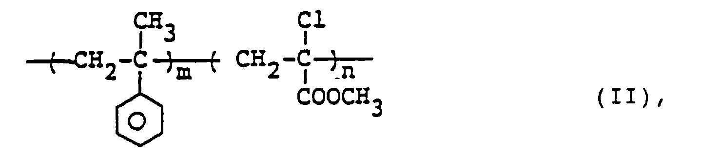
- the copolymer of formula I is not a copolymer represented by the formula (II): in which m and n are as defined above, and the developer consists substantially or completely of xylene, Then development takes place for from 10 to 20 minutes.
- the copolymer of the resist material is represented by the formula (II): in which n and m are defined above, and the developer is a hydrocarbon solvent exclusive of xylene or a ketone solvent.
- a process for the formation of resist patterns which, in addition to the above-described steps of formation of resist patterns, selective or pattern-wise exposure and development, further comprises the step of rinsing after the development with a rinsing solution which consists of at least one solvent capable of dissolving off a resist residue in the exposed area of the resist, but incapable of substantially dissolving the remaining resist in an unexposed area of the resist.
- the above-described resist material is applied to a substrate such as silicon or quartz.
- the resist material is preferably coated from a solution thereof onto the substrate. Any conventional coating techniques such as spin coating, dip coating or brush coating may be used herein. Note, if desired, other underlying materials including layers or coatings may be used in place of the semiconductor substrate.
- the resulting resist coating is exposed to a pattern of radiations, to conduct a selective exposure of the same.
- Any conventional ionizing radiations may be used as the exposure source, and suitable examples of the radiations include electron beam, X-rays and deep UV rays. Commercially available exposure apparatuses may be used to conduct this selective or pattern-wise exposure.
- the pattern-wise exposed resist is then developed in accordance with the manner of the present invention to selectively remove an exposed area.
- the development of the resist is carried out in accordance with two different methods, depending on the specific developer used.
- the pattern-wise exposed resist is developed with a developer which essentially consists of xylene, for 10 to 20 minutes.
- a developer which essentially consists of xylene
- the inventors found that the development time of 10 to 20 minutes is long enough to prevent a reduction of the layer thickness in an unexposed area while retaining a highly increased sensitivity.
- the exposed resist coating is developed with a developer which essentially consists of at least one solvent selected from the group consisting of aromatic hydrocarbon solvents exclusive of xylene, and ketone solvents.
- ketone solvents used herein is intended to mean any solvents containing at least one carbonyl (CO) group in a molecule thereof.
- Suitable aromatic hydrocarbon solvents include, for example, toluene, ethylbenzene or a mixture thereof with xylene
- suitable ketone solvents include, for example, methyl ethyl ketone, methyl isobutyl ketone, cyclohexanone or a mixture thereof.
- developer development time ethylbenzene 3 to 15 min. toluene 1 to 3 min. toluene/xylene (1:1) 1 to 5 min. cyclohexanone 5 to 10 min. methyl ethyl ketone (MEK) 10 to 15 sec.
- a pattern formation process of the present invention is generally stopped after a series of processings described above, but to remove the resist residues in the exposed area, it is preferable to rinse the developed resist coating with a rinsing solvent which consists of at least one solvent capable of dissolving off a resist residue in the exposed area, but incapable of substantially dissolving an unexposed area.
- a rinsing solvent which consists of at least one solvent capable of dissolving off a resist residue in the exposed area, but incapable of substantially dissolving an unexposed area.
- solvents suitably used as the rinsing solvent include carbon tetrachloride, xylene, methyl isobutyl ketone, isopropyl alcohol or a mixture thereof. Of course, other solvents may be used as the rinsing solvent, if desired.
- the present invention is directed to the selection of a suitable developer and to the choosing of a suitable development time, to thereby increase a sensitivity of the resist and obtain other effects of the present invention.
- the process of the present invention is an improvement of the resist process disclosed in the above-cited Japanese Kokai 63-137227.
- sensitivity of the resist can be increased if the developing time is extended, but for a positive-working resist material, the resolution thereof is undesirably reduced with an increase of the developing time. This is because the resist material in an unexposed area of the resist is dissolved off with the developer, and thus the layer thickness of the unexposed area is reduced.
- the resist materials used herein are the following three copolymers of ⁇ -methylstyrene and ⁇ -chloroacrylic methyl ester (1:1):
- Each resist material (Resist I, II or III) was dissolved in o-dichlorobenzene to prepare a resist solution.
- the resist solution was then spun-coated at a thickness of 5 ⁇ 10 -7 m (5000 ⁇ ) on a silicon substrate, and baked at 180°C for 20 minutes in an oven.
- the resulting resist coating was selectively exposed to an electron beam at an accelerated voltage of 20 kV on an electron beam exposure apparatus "ERE 301" commercially available from Erionics Co., and then developed with a developer described in the following Table 2, 3 or 4 relating to copolymers I, II and III respectively.
- the resulting resist patterns were evaluated to determine the suitable developing time at which the maximum sensitivity is obtained with regard to each developer.
- the 1,4-dioxane as the developer showed an unacceptably large reduction of the layer thickness in the unexposed area; pentoxone showed a bad sensitivity; and, n-propyl acetate produced the residues of the resist in the exposed area after development.
- developer developing time sensitivity results toluene 5 min. 8.8 good MEK 45 sec. 7.9 good MEK/MIBK (2:1) 2 min. 7.8 good MEK/MIBK (3:2) 2 min. 9.9 good 1,4-dioxane 1 min. 11.2 bad MIBK .... abbreviation of methyl isobutyl ketone
- the developing conditions applied to the pattern formation process of the present invention are considered to be very strong, because when the developer used is rapidly evaporated off by, for example, blowing nitrogen (N 2 ) gas or spinning off, the resist material or copolymer dissolved in the developer remains as a residue in the exposed area.
- a suitable rinsing solvent generally, a solvent or a mixture thereof incapable of dissolving the copolymer used as the resist material is used; such rinsing solvents, however, have a tendency to produce the resist residue, as a result of a remarkable reduction of solubility for the copolymer.
- a solution which consists of at least one solvent capable of dissolving off a resist residue in the exposed area, but incapable of substantially dissolving the unexposed area is suitable as the rinsing solvent.
- the solvents useful as the rinsing solvent are considered to be classified into a group between "good solvents” for the resist used and "bad solvents” for the resist used. The most satisfactory results are obtained when carbon tetrachroride, xylene, methyl isobutyl ketone (MIBK) or a mixture of MIBK and isopropyl alcohol (IPA) is used as the rinsing solvent.
- MIBK methyl isobutyl ketone
- IPA isopropyl alcohol
- the resist coating was exposed to a predetermined pattern of an electron beam, at an accelerated voltage of 20 kV and an exposure level of 12.0 ⁇ C/cm 2 on an EB exposure apparatus "ERE 301" commercially available from Erionics Co., and the exposed resist was then developed with xylene as a developer, for 20 minutes. Satisfactory fine resist patterns having a resolution of 2 ⁇ m line & space were obtained.
- the quartz substrate having the resist patterns on the surface thereof was placed in a reactive ion etching (RIE) apparatus, and using a mixture of CCl 4 and O 2 (1:1) as an etching gas and the resist patterns as a masking means, the underlying chromium layer was dry-etched for 6 minutes at a pressure of 0.2 Torr and 13.56 MHzRF power of 500 W.
- the resist patterns were exactly transferred to the underlying chromium layer, and this result indicates that the resist patterns have an excellent resistance to dry etching.
- Example 1 The procedure of the Example 1 was repeated, except that the exposure dosage was reduced to 11.5 ⁇ C/cm 2 , and the development was made with toluene (in place of xylene) for one minutes. Similar satisfactory fine resist patterns having a resolution of 2 ⁇ m line & space were obtained.
- Example 2 the reactive ion etching was carried out as in Example 1, and the resist patterns were exactly transferred to the underlying chromium layer.
- Example 1 The procedure of Example 1 was repeated, except that the exposure dosage was increased to 16.0 ⁇ C/cm 2 , and the development was made with cyclohexanone (in place of xylene) for 5 minutes. Similarly, satisfactory fine resist patterns having a resolution power of 2 ⁇ m line & space were obtained.
- the reactive ion etching was carried out as in the Example 1, and the resist patterns were exactly transferred to the underlying chromium layer.
- the resist was exposed to a predetermined pattern of an electron beam at an accelerated voltage of 20 kV on an EB exposure apparatus "ERE 301" commercially available from Erionics Co., and the exposed resist was then spray-developed with ethylbenzene as a developer for 10 minutes.
- the patterned resist was rinsed with a solvent described in Table 6 as a rinsing solution, for 60 seconds, and after the rinsing, the resist patterns were each quantitatively evaluated to ascertain whether or not a resist residue was formed.
- Table 6 rinsing solution resist residue xylene No carbon tetrachloride No MIBK No MIBK/IPA (9:1) No MIBK/IPA (5:5) No acetone Yes isooctane Yes cyclohexane/ethylbenzene (1:1) Yes IPA Yes No (control) Yes
- present invention provides an improved process for the formation of resist patterns, which process ensures a greatly increased sensitivity without thermal deformation of the resulting fine resist patterns.
- the present invention yields an improved process which also enables a complete removal of resist residues in an exposed area of the resist coating, in addition to the above-described prevention of the reduction of layer thickness. This is because, in the formation of highly dense resist patterns, resist residues are liable to be produced in an exposed area of the resist coating.
Landscapes
- Physics & Mathematics (AREA)
- General Physics & Mathematics (AREA)
- Spectroscopy & Molecular Physics (AREA)
- Photosensitive Polymer And Photoresist Processing (AREA)
- Exposure Of Semiconductors, Excluding Electron Or Ion Beam Exposure (AREA)
Claims (8)
- Verfahren zur Bildung von Resistmustern, welches die Schritte umfaßt:dadurch gekennzeichnet, daß das Resistmaterial aus einem Copolymer von α-Alkylstyrol und α-Halogenacrylester der Formel (I) besteht:Aufbringen eines positivarbeitenden Resistmaterials auf einem Substrat;Belichten des erhaltenen Überzugs des Resistmaterials mit einem Strahlungsmuster; undEntwickeln des gemustert belichteten Resists mit einem Entwickler, um das Resist in einem belichteten Bereich davon zu entfernen;worin R1 eine substituierte oder unsubstituierte nied.Alkyl-Gruppe bedeutet, R2 eine unsubstituierte nied.Alkyl-Gruppe darstellt, X ein Halogenatom ist, und m und n jeweils größer sind als Null und kleiner als 100, und
 das belichtete Resist mit einem aromatischen Kohlenwasserstoff oder einem Keton entwickelt wird,mit der Maßgabe, daß, wenn in der genannten Formel (I) R1 und R2 Methyl bedeuten, und X Chlor darstellt, und der Entwickler im wesentlichen oder vollständig aus Xylol besteht, die Entwicklung 10 bis 20 Minuten lang stattfindet.
 - Verfahren nach Anspruch 1, dadurch gekennzeichnet, daß das Copolymer der Formel (I) kein Copolymer der Formel (II) ist:worin m und n wie oben definiert sind, und der Entwickler im wesentlichen oder vollständig aus Xylol besteht, und dann die Entwicklung 10 bis 20 Minuten lang stattfindet.
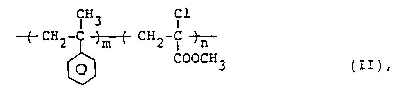
- Verfahren nach Anspruch 1, dadurch gekennzeichnet, daß das Copolymer des Resistmaterials die Formel (II) aufweist:worin m und n wie oben definiert sind, und der Entwickler ein aromatisches Kohlenwasserstoff-Lösungsmittel, ausgenommen Xylol, oder ein Keton-Lösungsmittel ist.
- Verfahren nach Anspruch 1, bei welchem der Entwickler ein aromatisches Kohlenwasserstoff-Lösungsmittel, ausgenommen Xylol, oder ein Keton-Lösungsmittel ist, und das belichtete Resist mit dem ausgewählten Entwickler 10 Sekunden bis 15 Minuten lang entwickelt wird.
- Verfahren nach Anspruch 1, 2, 3 oder 4, dadurch gekennzeichnet, daß Elektronenstrahl-Strahlung für die Belichtung verwendet wird.
- Verfahren nach einem der vorhergehenden Ansprüche, dadurch gekennzeichnet, daß es ferner den Schritt des Spülens des entwickelten Resists mit einem Spül-Lösungsmittel umfaßt, das aus Tetrachlorkohlenstoff, Xylol, Methylisobutylketon oder einer Mischung davon besteht.
- Verfahren nach einem der Ansprüche 1 und 3 bis 6, dadurch gekennzeichnet, daß das aromatische Kohlenwasserstoff-Lösungsmittel Toluol, Ethylbenzol oder eine Mischung davon mit Xylol ist.
- Verfahren nach einem der Ansprüche 1 und 3 bis 6, dadurch gekennzeichnet, daß das Keton-Lösungsmittel Methylethylketon, Methylisobutylketon, Cyclohexanon oder eine Mischung davon ist.
Applications Claiming Priority (4)
| Application Number | Priority Date | Filing Date | Title |
|---|---|---|---|
| JP272514/89 | 1989-10-19 | ||
| JP1272514A JP2867479B2 (ja) | 1989-10-19 | 1989-10-19 | レジストパターンの形成方法 |
| JP323024/89 | 1989-12-13 | ||
| JP1323024A JP2867509B2 (ja) | 1989-12-13 | 1989-12-13 | レジストパターンの形成方法 |
Publications (3)
| Publication Number | Publication Date |
|---|---|
| EP0424182A2 EP0424182A2 (de) | 1991-04-24 |
| EP0424182A3 EP0424182A3 (en) | 1991-12-11 |
| EP0424182B1 true EP0424182B1 (de) | 1998-07-08 |
Family
ID=26550240
Family Applications (1)
| Application Number | Title | Priority Date | Filing Date |
|---|---|---|---|
| EP90311533A Expired - Lifetime EP0424182B1 (de) | 1989-10-19 | 1990-10-19 | Verfahren zur Herstellung von Photolackmustern |
Country Status (3)
| Country | Link |
|---|---|
| US (1) | US5403699A (de) |
| EP (1) | EP0424182B1 (de) |
| DE (1) | DE69032464T2 (de) |
Cited By (1)
| Publication number | Priority date | Publication date | Assignee | Title |
|---|---|---|---|---|
| US6485890B2 (en) | 1996-04-23 | 2002-11-26 | Kodak Polychrome Graphics, Llc | Lithographic printing forms |
Families Citing this family (12)
| Publication number | Priority date | Publication date | Assignee | Title |
|---|---|---|---|---|
| US6117610A (en) * | 1997-08-08 | 2000-09-12 | Kodak Polychrome Graphics Llc | Infrared-sensitive diazonaphthoquinone imaging composition and element containing non-basic IR absorbing material and methods of use |
| US6063544A (en) * | 1997-03-21 | 2000-05-16 | Kodak Polychrome Graphics Llc | Positive-working printing plate and method of providing a positive image therefrom using laser imaging |
| US6090532A (en) * | 1997-03-21 | 2000-07-18 | Kodak Polychrome Graphics Llc | Positive-working infrared radiation sensitive composition and printing plate and imaging method |
| BR9810545A (pt) | 1997-07-05 | 2000-09-05 | Kodak Polychrome Graphics Llc | Métodos para a formação de configuração |
| US6060217A (en) * | 1997-09-02 | 2000-05-09 | Kodak Polychrome Graphics Llc | Thermal lithographic printing plates |
| US6221568B1 (en) * | 1999-10-20 | 2001-04-24 | International Business Machines Corporation | Developers for polychloroacrylate and polychloromethacrylate based resists |
| TWI281101B (en) | 2000-02-28 | 2007-05-11 | Mitsubishi Electric Corp | Developing process, process for forming pattern and process for preparing semiconductor device using same |
| DE10153496B4 (de) * | 2001-10-31 | 2007-01-04 | Infineon Technologies Ag | Verfahren zur Aromatisierung und Cycloaliphatisierung von Fotoresists im UV-Bereich |
| WO2016132722A1 (ja) * | 2015-02-20 | 2016-08-25 | 日本ゼオン株式会社 | 重合体およびポジ型レジスト組成物 |
| KR20170120590A (ko) * | 2015-02-20 | 2017-10-31 | 니폰 제온 가부시키가이샤 | 중합체 및 포지티브형 레지스트 조성물 |
| JP6379292B2 (ja) | 2015-06-23 | 2018-08-22 | 富士フイルム株式会社 | リンス液、パターン形成方法、及び電子デバイスの製造方法 |
| JP5938536B1 (ja) * | 2016-03-25 | 2016-06-22 | 日本ゼオン株式会社 | 共重合体の製造方法 |
Family Cites Families (6)
| Publication number | Priority date | Publication date | Assignee | Title |
|---|---|---|---|---|
| CA1164261A (en) * | 1981-04-21 | 1984-03-27 | Tsukasa Tada | PROCESS FOR FORMING RESIST PATTERNS BY DEVELOPING A POLYMER CONTAINING TRIFLUOROETHYL-.alpha.- CHLOROCRYLATE UNITS WITH SPECIFIC KETONE COMPOUNDS |
| JPS5999720A (ja) * | 1982-11-30 | 1984-06-08 | Toshiba Corp | レジスト像形成方法 |
| EP0230656B1 (de) * | 1985-12-25 | 1991-03-13 | Tosoh Corporation | Halogen enthaltende Polyacrylat-Derivate |
| JPH083636B2 (ja) * | 1986-11-29 | 1996-01-17 | 富士通株式会社 | 電子線ポジレジスト |
| JPS63273856A (ja) * | 1987-05-01 | 1988-11-10 | Oki Electric Ind Co Ltd | レジストパタ−ンの形成方法 |
| DE69015381T2 (de) * | 1989-03-03 | 1995-05-04 | Fujitsu Ltd | Herstellungsverfahren für ein Halbleiter-Bauelement und musterbildende Beschichtungslösung dafür. |
-
1990
- 1990-10-19 EP EP90311533A patent/EP0424182B1/de not_active Expired - Lifetime
- 1990-10-19 DE DE69032464T patent/DE69032464T2/de not_active Expired - Lifetime
-
1993
- 1993-08-02 US US08/100,343 patent/US5403699A/en not_active Expired - Lifetime
Cited By (1)
| Publication number | Priority date | Publication date | Assignee | Title |
|---|---|---|---|---|
| US6485890B2 (en) | 1996-04-23 | 2002-11-26 | Kodak Polychrome Graphics, Llc | Lithographic printing forms |
Also Published As
| Publication number | Publication date |
|---|---|
| DE69032464D1 (de) | 1998-08-13 |
| EP0424182A3 (en) | 1991-12-11 |
| US5403699A (en) | 1995-04-04 |
| EP0424182A2 (de) | 1991-04-24 |
| DE69032464T2 (de) | 1998-11-12 |
Similar Documents
| Publication | Publication Date | Title |
|---|---|---|
| US6723488B2 (en) | Photoresist composition for deep UV radiation containing an additive | |
| EP0232972B1 (de) | Negativ arbeitende Photolack-Zusammensetzung und Verfahren zur Herstellung von thermisch stabilen negativen Bildern damit | |
| TWI408493B (zh) | 光罩基板用光阻下層膜形成組成物,光罩基板及光罩 | |
| JP3748596B2 (ja) | レジスト材料及びレジストパターンの形成方法 | |
| US4405708A (en) | Method of applying a resist pattern on a substrate, and resist material mixture | |
| US5403699A (en) | Process for formation of resist patterns | |
| KR20040035782A (ko) | 에칭 방법 및 에칭 보호층 형성용 조성물 | |
| EP1466215A1 (de) | Negative duv photolack | |
| US5688634A (en) | Energy sensitive resist material and process for device fabrication using the resist material | |
| CA2074791A1 (en) | Negative-working radiation-sensitive mixture and radiation-sensitive recording material produced therewith | |
| JP3433153B2 (ja) | パターン形成材料、パターン形成方法、及び露光用マスクの製造方法 | |
| JP2867479B2 (ja) | レジストパターンの形成方法 | |
| EP0025633A1 (de) | Verfahren zum Anbringen einer Schicht auf einem Substrat gemäss einem Muster | |
| JP3779882B2 (ja) | 現像方法、パターン形成方法およびこれらを用いたフォトマスクの製造方法、半導体装置の製造方法 | |
| JP3507219B2 (ja) | ネガ型レジスト組成物及びパターン形成方法 | |
| JP2001318472A5 (de) | ||
| US4588675A (en) | Method for fine pattern formation on a photoresist | |
| US4608281A (en) | Improvements in sensitivity of a positive polymer resist having a glass transition temperature through control of a molecular weight distribution and prebaked temperature | |
| US4304840A (en) | Method of delineating a desired integrated circuit pattern upon a circuit substrate | |
| JPH0643631A (ja) | 非イオン性ポリグリコールを含有するフォトレジスト | |
| JPS59124133A (ja) | ネガテイブ型レジスト像の形成方法 | |
| WO2001022170A1 (fr) | Procede de formation d'un motif de resist presentant une resistance amelioree a la gravure seche | |
| JPH0381143B2 (de) | ||
| JP3628135B2 (ja) | 化学増幅型レジストおよびパターン形成方法 | |
| JPS61241745A (ja) | ネガ型フオトレジスト組成物及びレジストパタ−ン形成方法 |
Legal Events
| Date | Code | Title | Description |
|---|---|---|---|
| PUAI | Public reference made under article 153(3) epc to a published international application that has entered the european phase |
Free format text: ORIGINAL CODE: 0009012 |
|
| AK | Designated contracting states |
Kind code of ref document: A2 Designated state(s): DE FR GB |
|
| PUAL | Search report despatched |
Free format text: ORIGINAL CODE: 0009013 |
|
| AK | Designated contracting states |
Kind code of ref document: A3 Designated state(s): DE FR GB |
|
| 17P | Request for examination filed |
Effective date: 19920604 |
|
| 17Q | First examination report despatched |
Effective date: 19950810 |
|
| GRAG | Despatch of communication of intention to grant |
Free format text: ORIGINAL CODE: EPIDOS AGRA |
|
| GRAG | Despatch of communication of intention to grant |
Free format text: ORIGINAL CODE: EPIDOS AGRA |
|
| GRAH | Despatch of communication of intention to grant a patent |
Free format text: ORIGINAL CODE: EPIDOS IGRA |
|
| GRAH | Despatch of communication of intention to grant a patent |
Free format text: ORIGINAL CODE: EPIDOS IGRA |
|
| GRAA | (expected) grant |
Free format text: ORIGINAL CODE: 0009210 |
|
| AK | Designated contracting states |
Kind code of ref document: B1 Designated state(s): DE FR GB |
|
| PG25 | Lapsed in a contracting state [announced via postgrant information from national office to epo] |
Ref country code: FR Free format text: LAPSE BECAUSE OF FAILURE TO SUBMIT A TRANSLATION OF THE DESCRIPTION OR TO PAY THE FEE WITHIN THE PRESCRIBED TIME-LIMIT Effective date: 19980708 |
|
| REF | Corresponds to: |
Ref document number: 69032464 Country of ref document: DE Date of ref document: 19980813 |
|
| RIN2 | Information on inventor provided after grant (corrected) |
Free format text: TAKECHI, SATOSHI * NAKAMURA, YUKO * KOTACHI, AKIKO |
|
| PG25 | Lapsed in a contracting state [announced via postgrant information from national office to epo] |
Ref country code: GB Free format text: LAPSE BECAUSE OF NON-PAYMENT OF DUE FEES Effective date: 19981019 |
|
| EN | Fr: translation not filed | ||
| PLBE | No opposition filed within time limit |
Free format text: ORIGINAL CODE: 0009261 |
|
| STAA | Information on the status of an ep patent application or granted ep patent |
Free format text: STATUS: NO OPPOSITION FILED WITHIN TIME LIMIT |
|
| GBPC | Gb: european patent ceased through non-payment of renewal fee |
Effective date: 19981019 |
|
| 26N | No opposition filed | ||
| PGFP | Annual fee paid to national office [announced via postgrant information from national office to epo] |
Ref country code: DE Payment date: 20091015 Year of fee payment: 20 |
|
| PG25 | Lapsed in a contracting state [announced via postgrant information from national office to epo] |
Ref country code: DE Free format text: LAPSE BECAUSE OF EXPIRATION OF PROTECTION Effective date: 20101019 |