EP0425076A2 - Procédé pour la fabrication des puces à optique intégrée à coefficients électro-optiques élevés - Google Patents
Procédé pour la fabrication des puces à optique intégrée à coefficients électro-optiques élevés Download PDFInfo
- Publication number
- EP0425076A2 EP0425076A2 EP90308085A EP90308085A EP0425076A2 EP 0425076 A2 EP0425076 A2 EP 0425076A2 EP 90308085 A EP90308085 A EP 90308085A EP 90308085 A EP90308085 A EP 90308085A EP 0425076 A2 EP0425076 A2 EP 0425076A2
- Authority
- EP
- European Patent Office
- Prior art keywords
- chip
- proton
- chip substrate
- exchanged
- microcracking
- Prior art date
- Legal status (The legal status is an assumption and is not a legal conclusion. Google has not performed a legal analysis and makes no representation as to the accuracy of the status listed.)
- Ceased
Links
- 238000000034 method Methods 0.000 title claims abstract description 28
- 239000000758 substrate Substances 0.000 claims abstract description 45
- 238000000137 annealing Methods 0.000 claims abstract description 25
- 229910052739 hydrogen Inorganic materials 0.000 claims abstract description 20
- 239000001257 hydrogen Substances 0.000 claims abstract description 20
- -1 hydrogen ions Chemical class 0.000 claims abstract description 18
- GQYHUHYESMUTHG-UHFFFAOYSA-N lithium niobate Chemical group [Li+].[O-][Nb](=O)=O GQYHUHYESMUTHG-UHFFFAOYSA-N 0.000 claims abstract description 17
- WPYMKLBDIGXBTP-UHFFFAOYSA-N benzoic acid Chemical compound OC(=O)C1=CC=CC=C1 WPYMKLBDIGXBTP-UHFFFAOYSA-N 0.000 claims abstract description 12
- 239000002253 acid Substances 0.000 claims abstract description 11
- 239000001301 oxygen Substances 0.000 claims abstract description 10
- 229910052760 oxygen Inorganic materials 0.000 claims abstract description 10
- QVGXLLKOCUKJST-UHFFFAOYSA-N atomic oxygen Chemical compound [O] QVGXLLKOCUKJST-UHFFFAOYSA-N 0.000 claims abstract description 9
- 239000005711 Benzoic acid Substances 0.000 claims abstract description 6
- 235000010233 benzoic acid Nutrition 0.000 claims abstract description 6
- UFHFLCQGNIYNRP-UHFFFAOYSA-N Hydrogen Chemical compound [H][H] UFHFLCQGNIYNRP-UHFFFAOYSA-N 0.000 claims description 4
- 238000009792 diffusion process Methods 0.000 claims description 3
- 239000000126 substance Substances 0.000 claims description 3
- 230000008878 coupling Effects 0.000 claims description 2
- 238000010168 coupling process Methods 0.000 claims description 2
- 238000005859 coupling reaction Methods 0.000 claims description 2
- 239000000835 fiber Substances 0.000 claims description 2
- 239000007789 gas Substances 0.000 claims description 2
- 230000003287 optical effect Effects 0.000 claims description 2
- 229910052805 deuterium Inorganic materials 0.000 claims 2
- 235000012431 wafers Nutrition 0.000 description 30
- 230000000873 masking effect Effects 0.000 description 6
- HBBGRARXTFLTSG-UHFFFAOYSA-N Lithium ion Chemical compound [Li+] HBBGRARXTFLTSG-UHFFFAOYSA-N 0.000 description 5
- 229910001416 lithium ion Inorganic materials 0.000 description 5
- 229910052782 aluminium Inorganic materials 0.000 description 2
- 238000010586 diagram Methods 0.000 description 2
- WSMQKESQZFQMFW-UHFFFAOYSA-N 5-methyl-pyrazole-3-carboxylic acid Chemical compound CC1=CC(C(O)=O)=NN1 WSMQKESQZFQMFW-UHFFFAOYSA-N 0.000 description 1
- VYZAMTAEIAYCRO-UHFFFAOYSA-N Chromium Chemical compound [Cr] VYZAMTAEIAYCRO-UHFFFAOYSA-N 0.000 description 1
- 229910012463 LiTaO3 Inorganic materials 0.000 description 1
- 238000010306 acid treatment Methods 0.000 description 1
- 150000007513 acids Chemical class 0.000 description 1
- AZDRQVAHHNSJOQ-UHFFFAOYSA-N alumane Chemical compound [AlH3] AZDRQVAHHNSJOQ-UHFFFAOYSA-N 0.000 description 1
- XAGFODPZIPBFFR-UHFFFAOYSA-N aluminium Chemical compound [Al] XAGFODPZIPBFFR-UHFFFAOYSA-N 0.000 description 1
- 150000001450 anions Chemical class 0.000 description 1
- 230000015572 biosynthetic process Effects 0.000 description 1
- 238000004140 cleaning Methods 0.000 description 1
- 238000010438 heat treatment Methods 0.000 description 1
- 150000002431 hydrogen Chemical class 0.000 description 1
- GPRLSGONYQIRFK-UHFFFAOYSA-N hydron Chemical group [H+] GPRLSGONYQIRFK-UHFFFAOYSA-N 0.000 description 1
- 238000005342 ion exchange Methods 0.000 description 1
- 239000013307 optical fiber Substances 0.000 description 1
- 150000002926 oxygen Chemical class 0.000 description 1
- 238000004806 packaging method and process Methods 0.000 description 1
- 238000000206 photolithography Methods 0.000 description 1
Images

Classifications
-
- G—PHYSICS
- G02—OPTICS
- G02B—OPTICAL ELEMENTS, SYSTEMS OR APPARATUS
- G02B6/00—Light guides; Structural details of arrangements comprising light guides and other optical elements, e.g. couplings
- G02B6/10—Light guides; Structural details of arrangements comprising light guides and other optical elements, e.g. couplings of the optical waveguide type
- G02B6/12—Light guides; Structural details of arrangements comprising light guides and other optical elements, e.g. couplings of the optical waveguide type of the integrated circuit kind
- G02B6/13—Integrated optical circuits characterised by the manufacturing method
- G02B6/134—Integrated optical circuits characterised by the manufacturing method by substitution by dopant atoms
- G02B6/1345—Integrated optical circuits characterised by the manufacturing method by substitution by dopant atoms using ion exchange
Definitions
- This invention relates to processes for making multifunction integrated optics chips having optimally high electro-optic coefficients, and proton-exchanged, preferivelyably rhombohedral structure, and to the multifunction integrated optics chips resulting from these processes.
- the methods for making multifunction integrated optics chips have included the step of subjecting the chips to proton exchange with acids such as benzoic acid at temperatures in the range of about 150°C to about 250°C for times of about 10 to about 20 minutes or more.
- acids such as benzoic acid
- the lithium niobate substrates tend to form substantial internal stresses that result in microcracking in the substrate areas exposed to the proton exchange step.
- the chips made by processes including this step frequently exhibit refractive index instabilities, high propagation losses, and low electro-optic coefficients.
- This invention provides methods for making proton-exchanged, multifunction integrated optics chips (MIOCS) that are, in preferred embodiments, based on the stable rhombohedral Li 1-x H x NbO3 structure. These chips have substantially diffused protons, are substantially free of microcracking and of internal stresses that can result in microcracking, and yet have optimally high electro-optic coefficients. These methods are particularly adapted for making such chips from proton-exchanged lithium niobate.
- MIOCS multifunction integrated optics chips
- a method for making proton-exchanged integrated optics chips comprising treating a chip substrate with a proton-exchanging acid at a temperature and for a time sufficient to cause substantial proton exchange at and below the surface of said chip substrate, but for a time insufficient to create any microcracking or internal stresses that lead to microcracking in said chip substrate; thermally annealing said chip substrate in the presence of oxygen at a temperature and for a time sufficient to diffuse the hydrogen ions at and near the surface of said chip substrate substantially below the surface of said chip substrate, and for a time and at a temperature sufficient to restore and to optimize the electro-optic coefficient of said chip substrate.
- the method may include the steps of: forming a multifunction integrated optics chip substrate from a substrate adapted for this purpose such as lithium niobate; affixing a removable mask or mask pattern to at least one surface of the chip substrate to form one or more proton-exchanged patterns of desired size and shape at the surface of the chip; treating the masked chip with a proton-exchanging acid such as benzoic acid at a temperature and for a time sufficient to cause substantial proton exchange at and below the unmasked surface of the chip substrate, but for a time insufficient to create any microcracking or internal stresses that lead to microcracking in the chip substrate; removing the mask or mask pattern from the chip substrate; and thermally annealing the chip, in the presence of oxygen, at a temperature and for a time sufficient to diffuse the hydrogen ions at and near the surface of the chip substrate substantially below its surface, and for a time and at a temperature sufficient to restore and to optimize the electro-optic coefficient of the chip substrate.
- a proton-exchanging acid
- This invention also relates to multifunction integrated optics chips having a proton-exchanged lithium niobate surface or surface pattern of desired size and shape with the proton-exchanged hydrogen ions substantially diffused into and below the surface of the chip. These chips exhibit the stable rhombohedral structure and the smaller stresses that lead to microcracking and substantially free of microcracking in their proton-exchanged regions. These chips also have restored, optimized electro-optic coefficients substantially equal to the electro-optic coefficients of the chips before proton exchange begins.
- the multifunction integrated optics chips are formed of a substance such as lithium niobate. These chips can be of any desired size and shape and thickness. Alternatively, these chips can be made of substances such as LiTaO3 (lithium tantalate).
- the wafers to be converted to MIOCS are covered, on one or more of their surfaces, with a mask or masking pattern, such as a mask made of aluminum or chromium metal.
- a mask or masking pattern such as a mask made of aluminum or chromium metal.
- These masks preferably include a pattern of sufficient size and shape to form a desired pattern of electro-optic channels in the wafers.
- the lithium niobate wafers are treated with an acid eg benzoic acid that causes proton exchange between the hydrogen ions in the acid and the anions, e.g., lithium ions, in the wafers.
- the acid treatment takes place at elevated temperature, preferably in the range of about 100°C to about 250°C, and for a time in the range of a few minutes up to as many as 20 or even 30 minutes.
- the temperatures and times of proton exchange are, in general, sufficient to cause substantial proton exchange in the desired areas of the wafers, but sufficiently short to avoid the creation of stresses that lead to microcracking, or to the formation of microcracks, in the wafer regions exposed to proton exchange.
- the proton exchange step is preferably controlled so as to limit the depth of proton exchange below the surface of the wafer to not more than about 5 microns and preferably not more than about 2 microns.
- proton exchange time is preferably limited to no more than about 10 minutes up to about 15 minutes.
- the exchange time should preferably not exceed the time required to convert substantially 100% of the lithium ions to hydrogen ions at the surface of the wafer, and to convert substantially 100% of the lithium ions to hydrogen ions below the surface to a depth of not more than about 5 microns and preferably not more than about 2 microns.
- the wafer is heat-treated, i.e., thermally annealed, in an environment that contains more oxygen than air normally contains, and preferably in sufficient amounts and at sufficient temperatures and for sufficient times, to diffuse the hydrogen ions, formed at and near the surface of the chip, substantially into and below the surface of the chip.
- the heat treatment also converts the phase of the wafer, where the wafer is lithium niobate, from Perovskite, an unstable phase, to rhombohedral, a more stable phase.
- the annealing step is carried out for a time and at a temperature sufficient to reduce the hydrogen concentration at the surface of the wafer from about 100% to a value in the range of about 20% to about 30% and preferably less than about 25%.
- the annealing step is continued until the electro-optic coefficient of the wafer before proton exchange is substantially recovered, and optical propagation losses caused by proton exchange are reduced or substantially eliminated.
- the annealing step is, in some embodiments, carried out for a time sufficient to maximize the coupling between the waveguide in the wafer and the core of an optical fiber to be joined to the waveguide.
- the annealing is carried out until the spot size of light emerging from the core of a fiber to be coupled to the waveguide corresponds substantially to the spot size of light passing through and emerging from the waveguide itself.
- hydrogen diffusion into the waveguide will penetrate to a depth in the range of about 5 to about 7 microns.
- the annealing is carried out by increasing gradually the temperature of the annealing from room temperature, e.g., about 20°C, up to a desired maximum temperature, preferably in the range of about 325°C to about 375°C, over a time period of up to about 30 minutes, but preferably as rapidly as possible.
- the annealing continues at the maximum temperature for a time sufficient to cause the desired diffusion of hydrogen ions into the wafer and to restore the electro-optic coefficient of the wafer to optimum value, i.e., to a value at or near the value of the wafer before exposure to proton exchange and annealing.
- the annealing takes place in a chamber that is substantially impervious to gases and that is exposed to air or oxygen.
- oxygen flows into the annealing chamber at a rate in the range of about 0.1 litres per minute to about 0.4 litres per minute. This oxygen flow is maintained throughout the annealing step.
- Fig. 1 shows, in block diagram form, a preferred embodiment of the methods of this invention.
- a lithium niobate wafer after cleaning in step 1 passes via path 2 to masking step 3.
- the masking comprises placing an aluminum mask, by photolithography, on the lithium niobate wafer to form a Y-junction pattern. From masking step 3, the masked lithium niobate wafer passes on path 4 to proton exchange step 5.
- the benzoic acid melt 16 impinges on the entire surface of masked wafer 17.
- mask 18 blocks all portions of the wafer except unmasked area 19
- hydrogen ion exchange for lithium ions is confined to area 19, preferably to a depth of about 2 microns below the surface of the wafer in area 19.
- hydrogen ions enter on path 20 and lithium ions leave on path 21.
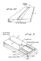
- the proton-exchanged wafer 17, after this step, includes proton-exchanged guiding region 19; see Fig. 2B.
- proton-exchanged, masked lithium niobate wafer 17 passes on path 6 to thermal annealing step 7.
- the masked substrate is subjected to thermal annealing at a temperature that gradually increases from about 20°C up to a desired maximum that is preferably in the range of about 325°C to about 375°C over a period of up to about 30 minutes, but preferably as quickly as possible.
- the annealing causes hydrogen ions to diffuse into the wafer in the proton-exchanged area to a depth in the range of about five to about seven microns.
- the wafer passes on path 8 to photolithographic step 9 where, using conventional photolithographic processes, electrodes are formed on the substrate.
- the wafer then passes on path 10 to a dicing and packaging step 11 where the wafer is cut into products of desired size and shape before passing on path 12 to finishing step 13.
- Fig. 3 shows a preferred embodiment of a finished product with the hydrogen ion-exchanged, thermally annealed, Y-shaped polarizing waveguide 14 formed on the surface of wafer 15.
Landscapes
- Physics & Mathematics (AREA)
- Engineering & Computer Science (AREA)
- Microelectronics & Electronic Packaging (AREA)
- General Physics & Mathematics (AREA)
- Optics & Photonics (AREA)
- Optical Integrated Circuits (AREA)
- Optical Modulation, Optical Deflection, Nonlinear Optics, Optical Demodulation, Optical Logic Elements (AREA)
Applications Claiming Priority (2)
| Application Number | Priority Date | Filing Date | Title |
|---|---|---|---|
| US42817489A | 1989-10-27 | 1989-10-27 | |
| US428174 | 1989-10-27 |
Publications (2)
| Publication Number | Publication Date |
|---|---|
| EP0425076A2 true EP0425076A2 (fr) | 1991-05-02 |
| EP0425076A3 EP0425076A3 (en) | 1991-10-30 |
Family
ID=23697847
Family Applications (1)
| Application Number | Title | Priority Date | Filing Date |
|---|---|---|---|
| EP19900308085 Ceased EP0425076A3 (en) | 1989-10-27 | 1990-07-24 | Process for making intergrated optics chips having high electro-optic coefficients |
Country Status (2)
| Country | Link |
|---|---|
| EP (1) | EP0425076A3 (fr) |
| JP (1) | JPH03153202A (fr) |
Cited By (3)
| Publication number | Priority date | Publication date | Assignee | Title |
|---|---|---|---|---|
| EP0518059A1 (fr) * | 1991-05-10 | 1992-12-16 | ALENIA AERITALIA & SELENIA S.P.A. | Fabrication de guides d'onde optiques en forme de sillon en LiNbO3 |
| EP0922793A3 (fr) * | 1997-11-25 | 2000-08-09 | Ngk Insulators, Ltd. | Méthode pour traiter un substrat de matériau ferroélectrique cristallin |
| DE10061831A1 (de) * | 2000-12-12 | 2002-06-13 | Wuerth Elektronik Gmbh | Optische Mehrlagenleiterplatte |
Family Cites Families (1)
| Publication number | Priority date | Publication date | Assignee | Title |
|---|---|---|---|---|
| US4547262A (en) * | 1984-08-30 | 1985-10-15 | Sperry Corporation | Method for forming thin film passive light waveguide circuit |
-
1990
- 1990-07-24 EP EP19900308085 patent/EP0425076A3/en not_active Ceased
- 1990-10-24 JP JP2288278A patent/JPH03153202A/ja active Pending
Cited By (4)
| Publication number | Priority date | Publication date | Assignee | Title |
|---|---|---|---|---|
| EP0518059A1 (fr) * | 1991-05-10 | 1992-12-16 | ALENIA AERITALIA & SELENIA S.P.A. | Fabrication de guides d'onde optiques en forme de sillon en LiNbO3 |
| EP0922793A3 (fr) * | 1997-11-25 | 2000-08-09 | Ngk Insulators, Ltd. | Méthode pour traiter un substrat de matériau ferroélectrique cristallin |
| DE10061831A1 (de) * | 2000-12-12 | 2002-06-13 | Wuerth Elektronik Gmbh | Optische Mehrlagenleiterplatte |
| DE10061831B4 (de) * | 2000-12-12 | 2014-02-13 | Würth Elektronik Rot am See GmbH & Co. KG | Optische Mehrlagenleiterplatte |
Also Published As
| Publication number | Publication date |
|---|---|
| JPH03153202A (ja) | 1991-07-01 |
| EP0425076A3 (en) | 1991-10-30 |
Similar Documents
| Publication | Publication Date | Title |
|---|---|---|
| US5193136A (en) | Process for making multifunction integrated optics chips having high electro-optic coefficients | |
| US4547262A (en) | Method for forming thin film passive light waveguide circuit | |
| US6374005B2 (en) | Integrated optic device produced by cyclically annealed proton exchange process | |
| US4196963A (en) | Method for eliminating Li2 O out-diffusion in LiNbO3 and LiTaO3 waveguide structures | |
| EP0635735A1 (fr) | Guides d'onde et modulateur de phase électro-optiques et procédés pour leur fabrication | |
| EP0380138B1 (fr) | Méthode de fabrication d'un guide d'ondes | |
| EP0425076A2 (fr) | Procédé pour la fabrication des puces à optique intégrée à coefficients électro-optiques élevés | |
| US4948407A (en) | Proton exchange method of forming waveguides in LiNbO3 | |
| CN100458478C (zh) | Y波导集成光学器件铌酸锂芯片的制备方法 | |
| EP0484796B1 (fr) | Dispositif de redoublement de la fréquence d'une onde lumineuse | |
| JPH0749428A (ja) | 光導波路の製造方法 | |
| GB2340957A (en) | Making proton-exchange waveguides | |
| US5000774A (en) | Method of masked two stage lithium niobate proton exchange | |
| CA2289876A1 (fr) | Methode de fabrication de guides d'ondes a echange de protons | |
| EP0340983B1 (fr) | Méthode d'échange de protons pour former des guides d'onde optiques | |
| JPS62293206A (ja) | 光素子の形成方法 | |
| JPH0756039A (ja) | プロトン交換導波路作製法 | |
| JPS6074441A (ja) | 半導体層の表面処理方法 | |
| Parmenter et al. | Fabrication of Titanium-In-Diffused Lithium Niobate Optical Waveguides by Laser Annealing at 10.6 μm | |
| JPS63158505A (ja) | テ−パ状導波路の作製方法 | |
| Chen | Diffusion Process for Formation of Single-Mode Waveguide. | |
| JPS6116530A (ja) | 半導体装置の製造方法 | |
| Hou et al. | Proton-exchanged optical waveguides in Y-cut MgO: LiNbO3 | |
| Anastassopoulou et al. | Characterization of benzoic acid ion exchange waveguides in lithium tantalate | |
| JPS60216335A (ja) | 光波長変換素子作製方法 |
Legal Events
| Date | Code | Title | Description |
|---|---|---|---|
| PUAI | Public reference made under article 153(3) epc to a published international application that has entered the european phase |
Free format text: ORIGINAL CODE: 0009012 |
|
| AK | Designated contracting states |
Kind code of ref document: A2 Designated state(s): DE FR GB IT |
|
| PUAL | Search report despatched |
Free format text: ORIGINAL CODE: 0009013 |
|
| AK | Designated contracting states |
Kind code of ref document: A3 Designated state(s): DE FR GB IT |
|
| 17P | Request for examination filed |
Effective date: 19920423 |
|
| 17Q | First examination report despatched |
Effective date: 19931220 |
|
| APAB | Appeal dossier modified |
Free format text: ORIGINAL CODE: EPIDOS NOAPE |
|
| APAD | Appeal reference recorded |
Free format text: ORIGINAL CODE: EPIDOS REFNE |
|
| APAB | Appeal dossier modified |
Free format text: ORIGINAL CODE: EPIDOS NOAPE |
|
| STAA | Information on the status of an ep patent application or granted ep patent |
Free format text: STATUS: THE APPLICATION HAS BEEN REFUSED |
|
| 18R | Application refused |
Effective date: 19980126 |
|
| APAF | Appeal reference modified |
Free format text: ORIGINAL CODE: EPIDOSCREFNE |