EP0425957A2 - Verfahren zum Herstellen einer Halbleitervorrichtung unter Verwendung eines Schrittes zum Isolierschichtätzen - Google Patents
Verfahren zum Herstellen einer Halbleitervorrichtung unter Verwendung eines Schrittes zum Isolierschichtätzen Download PDFInfo
- Publication number
- EP0425957A2 EP0425957A2 EP90120205A EP90120205A EP0425957A2 EP 0425957 A2 EP0425957 A2 EP 0425957A2 EP 90120205 A EP90120205 A EP 90120205A EP 90120205 A EP90120205 A EP 90120205A EP 0425957 A2 EP0425957 A2 EP 0425957A2
- Authority
- EP
- European Patent Office
- Prior art keywords
- insulating layer
- resist film
- forming
- semiconductor device
- manufacturing
- Prior art date
- Legal status (The legal status is an assumption and is not a legal conclusion. Google has not performed a legal analysis and makes no representation as to the accuracy of the status listed.)
- Withdrawn
Links
Images
Classifications
-
- H—ELECTRICITY
- H10—SEMICONDUCTOR DEVICES; ELECTRIC SOLID-STATE DEVICES NOT OTHERWISE PROVIDED FOR
- H10D—INORGANIC ELECTRIC SEMICONDUCTOR DEVICES
- H10D30/00—Field-effect transistors [FET]
- H10D30/01—Manufacture or treatment
- H10D30/015—Manufacture or treatment of FETs having heterojunction interface channels or heterojunction gate electrodes, e.g. HEMT
-
- H—ELECTRICITY
- H10—SEMICONDUCTOR DEVICES; ELECTRIC SOLID-STATE DEVICES NOT OTHERWISE PROVIDED FOR
- H10D—INORGANIC ELECTRIC SEMICONDUCTOR DEVICES
- H10D30/00—Field-effect transistors [FET]
- H10D30/01—Manufacture or treatment
- H10D30/061—Manufacture or treatment of FETs having Schottky gates
- H10D30/0612—Manufacture or treatment of FETs having Schottky gates of lateral single-gate Schottky FETs
-
- H—ELECTRICITY
- H10—SEMICONDUCTOR DEVICES; ELECTRIC SOLID-STATE DEVICES NOT OTHERWISE PROVIDED FOR
- H10D—INORGANIC ELECTRIC SEMICONDUCTOR DEVICES
- H10D64/00—Electrodes of devices having potential barriers
- H10D64/01—Manufacture or treatment
- H10D64/012—Manufacture or treatment of electrodes comprising a Schottky barrier to a semiconductor
- H10D64/0124—Manufacture or treatment of electrodes comprising a Schottky barrier to a semiconductor to Group III-V semiconductors
-
- H—ELECTRICITY
- H10—SEMICONDUCTOR DEVICES; ELECTRIC SOLID-STATE DEVICES NOT OTHERWISE PROVIDED FOR
- H10D—INORGANIC ELECTRIC SEMICONDUCTOR DEVICES
- H10D64/00—Electrodes of devices having potential barriers
- H10D64/01—Manufacture or treatment
- H10D64/012—Manufacture or treatment of electrodes comprising a Schottky barrier to a semiconductor
- H10D64/0124—Manufacture or treatment of electrodes comprising a Schottky barrier to a semiconductor to Group III-V semiconductors
- H10D64/0125—Manufacture or treatment of electrodes comprising a Schottky barrier to a semiconductor to Group III-V semiconductors characterised by the sectional shape, e.g. T or inverted T
-
- H—ELECTRICITY
- H10—SEMICONDUCTOR DEVICES; ELECTRIC SOLID-STATE DEVICES NOT OTHERWISE PROVIDED FOR
- H10P—GENERIC PROCESSES OR APPARATUS FOR THE MANUFACTURE OR TREATMENT OF DEVICES COVERED BY CLASS H10
- H10P50/00—Etching of wafers, substrates or parts of devices
- H10P50/73—Etching of wafers, substrates or parts of devices using masks for insulating materials
-
- H—ELECTRICITY
- H10—SEMICONDUCTOR DEVICES; ELECTRIC SOLID-STATE DEVICES NOT OTHERWISE PROVIDED FOR
- H10P—GENERIC PROCESSES OR APPARATUS FOR THE MANUFACTURE OR TREATMENT OF DEVICES COVERED BY CLASS H10
- H10P76/00—Manufacture or treatment of masks on semiconductor bodies, e.g. by lithography or photolithography
- H10P76/20—Manufacture or treatment of masks on semiconductor bodies, e.g. by lithography or photolithography of masks comprising organic materials
- H10P76/202—Manufacture or treatment of masks on semiconductor bodies, e.g. by lithography or photolithography of masks comprising organic materials for lift-off processes
Definitions
- This invention relates to a method of manufacturing a semiconductor device, which is applied to form a minute opening pattern (extraction pattern) having a diameter of 0.2 ⁇ m or less.
- EB (electron beam) drawing is widely employed as a method for forming a minute opening pattern with a diameter of 0.2 ⁇ m or less in an insulating layer and the like for constituting a semiconductor device.
- an insulating layer and the like are patterned using, in particular, a positive resist consisting of PMMA (polymethylmethacrylate) having high resolution.
- a multilayer resist process using a plurality of resist layers, or a method using an image-reversal process and a multilayer resist process are used to form a minute opening pattern.
- SPIE The Society of Photo-Optical Instrumentation Engineers
- Vol. 773 (1987) pages 61 to 67 discloses a method using an image-reversal process and a multilayer resist process.
- the resist consisting of PMMA and the like is not highly sensitive to light, a long period of time is required for drawing, and development conditions are also limited in detail. Hence, the throughput in manufacturing semiconductor devices by means of this method is low.
- the multilayer resist process requires a larger number of manufacturing steps than a single layer resist process.
- the dimensions of the top resist layer can be measured, the dimensions and configuration of lower resist layers cannot be measured unless the cross section is checked.
- the dimensions of the opening pattern can be measured by an SEM (scanning-type electronic microscope); however, to measure the dimensions of the cross section precisely, wafers must be broken in the PMMA resist process and in the multilayer resist process.
- the method of manufacturing a semiconductor device of the present invention comprises the steps of: forming a first insulating layer on a semiconductor substrate; forming a resist film sensitive to electron beams on the first insulating layer; applying electron beams onto a predetermined region of the resist film; removing unnecessary portions of the resist film by using a developer, thereby forming a remaining pattern resist film; forming a second insulating layer on the entire region of the first insulating layer and the remaining pattern resist film; simultaneously removing the remaining pattern resist film and the corresponding portion of the second insulating layer formed thereon, thereby forming an opening of a predetermined pattern in the second insulating layer; and etching the first insulating layer through the opening, using the second insulation layer as a mask, thereby exposing a predetermined region of the semiconductor substrate.
- a first insulating layer is formed on a semiconductor substrate, and a remaining pattern made of a negative resist is formed on the first insulating layer.
- a second insulating layer is formed on the entire region of the first insulating layer and on the remaining pattern. Thereafter, the negative resist is removed, forming an opening pattern in the second insulating layer.
- the first insulating layer is etched using the opening pattern formed on the second insulating layer as a mask, thereby forming an opening pattern in the first insulating layer.
- the dimensions of the opening pattern can be measured by measuring the dimensions of the remaining pattern.
- the remaining pattern is made of a negative resist, the resist is hardly damaged even when measurement is performed by an SEM. As a result, the dimensions of the opening pattern can be measured accurately. Further, since a negative resist is used, pattern drawing requires only a short period of time.
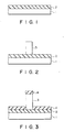
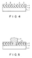
- Figs. 1 to 5 show in sequence the steps of manufacturing a semiconductor device according to an embodiment of the present invention.
- a substrate 1 is made of GaAs, or is constituted by a GaAs layer and an epitaxial layer of Al-GaAs formed thereon.
- a first insulating layer 2 made of, for example, Si3N4 is deposited to 500 ⁇ 1000 ⁇ thickness on the GaAs substrate 1 since, if the first insulating layer 2 is thinner than 500 ⁇ , it does not fulfill the function of protecting the surface of the GaAs substrate 1 from contamination and if it is thicker than 1000 ⁇ , a pattern conversion error in etching (to be described later) is large, and a long etching time is required.
- a negative resist film 3 made of, for example, a novolak resin (SAL601, Gypsy Corporation) which is sensitive to electron beams is formed 0.5 ⁇ m thick on the negative resist film 3.
- a predetermined pattern is drawn on the resist film 3 by an EB exposure device. The pattern is the inversion of the pattern to be ultimately formed on the resist film 3.
- a 0.1 ⁇ m wide remaining pattern of the resist film 3 is formed by developing treatment, and subjected to post-baking.
- a second insulating layer 4 made of, for example, SiO2 is deposited to a thickness of 500 - 1000 ⁇ over the entire first insulating layer 2 and the resist film 3 by sputtering, which enables deposition at a low temperature.
- the second insulating layer 4 is thinner than 500 ⁇ , it does not satisfactorily function as a mask, since the selection rate in an etching process (to be described later) cannot be set at a suitable value, and if the second insulating layer 4 is thicker than 1000 ⁇ , it is difficult to lift off the layer 4 and the resist film 3 together (to be described later). In consideration of this, it is desirable that the second insulating layer 4 has a thickness 60 ⁇ 70% that of the resist film 3.
- the remaining pattern of the resist film 3 and the second insulating film 4 formed thereon are removed by acetone or an ordinary resist lift-off solution.
- CDE chemical dry etching
- CF4 + O2 gas using the second insulating layer 4 as a mask
- electrode metal 5 is formed on the second insulating layer 4, such that it is brought into contact with a predetermined region of the GaAs substrate 1 via opening pattern 10.
- a gate electrode for use in a GaAs ⁇ FET, an HEMT, or the like is formed.
- a gate electrode for use in a GaAs ⁇ FET, an HEMT, or the like is formed in the same manner as in embodiment 1 through the steps shown in Figs. 1 to 5, except that the first insulating layer 2 and the second insulating layer 4 are respectively made of SiO2 and Si3N4, and the first insulating layer 2 is removed by means of an RIE method.
- a negative resist film 3 is formed on a first insulating layer 2, and a 0.1 ⁇ m wide remaining pattern of the resist film 3 is formed.
- a second insulating layer 4 made of Si3N4 is deposited to a thickness of 500 ⁇ 1000 ⁇ over the entire first insulating layer 2 and the resist film 3 by means of sputtering.
- the remaining pattern of the resist film 3 and the second insulating film 4 formed thereon are removed by acetone or an ordinary resist lift-off solution.
- the first insulating layer 2 is dry-etched by an RIE method using CF4 + O2 gas, thereby forming a 0.1 ⁇ m wide opening pattern 10 in the first insulating layer 2.
- electrode metal 5 is formed on the second insulating layer 4, such that it is brought into contact with a predetermined region of the GaAs substrate 1 via opening pattern 10.
- a gate electrode for use in a GaAs ⁇ FET, an HEMT, or the like is formed.
- the opening pattern 10 of 0.1 ⁇ m width is formed by the electron beams under the condition of an acceleration voltage of 50 KeV. In this case, when the dosage is 0.4nc/cm, a vertical profile is obtained.
- the dimensions of the negative resist film 3 were measured by means of end measuring SEM photography and cross-section measuring SEM photography, and errors were only 0.005 - 0.01 ⁇ m with a magnification of about 50,000.
- the drawing time can be reduced to 1/3 ⁇ 1/5 of that required where a positive resist film having a low sensitivity is used.
- an electrode metal is formed by a lift-off method immediately after etching is performed using SiO2 as a resist mask, and then the resist removing and cleaning are performed. For this reason, the electrode may be seriously damaged and contaminated.
- organic substances such as a resist rarely remain on the electrode or adversely affects it.
- a GaAs substrate is used as a semiconductor substrate; however, a silicon substrate or the like may be used instead.
- first and second insulating layers 2 and 4 may be made of the same material.
- the dimensions of the opening pattern can be measured easily by measuring the dimensions of the remaining pattern.
- the remaining pattern is made of a negative resist, the drawing time is short and the resist is hardly damaged even when measurement is performed by an SEM.
Landscapes
- Electron Beam Exposure (AREA)
- Exposure And Positioning Against Photoresist Photosensitive Materials (AREA)
- Photosensitive Polymer And Photoresist Processing (AREA)
- Internal Circuitry In Semiconductor Integrated Circuit Devices (AREA)
Applications Claiming Priority (2)
| Application Number | Priority Date | Filing Date | Title |
|---|---|---|---|
| JP274971/89 | 1989-10-24 | ||
| JP1274971A JPH03138938A (ja) | 1989-10-24 | 1989-10-24 | 半導体装置の製造方法 |
Publications (2)
| Publication Number | Publication Date |
|---|---|
| EP0425957A2 true EP0425957A2 (de) | 1991-05-08 |
| EP0425957A3 EP0425957A3 (en) | 1991-07-24 |
Family
ID=17549118
Family Applications (1)
| Application Number | Title | Priority Date | Filing Date |
|---|---|---|---|
| EP19900120205 Withdrawn EP0425957A3 (en) | 1989-10-24 | 1990-10-22 | Method of manufacturing a semiconductor device involving a step of patterning an insulating layer |
Country Status (3)
| Country | Link |
|---|---|
| EP (1) | EP0425957A3 (de) |
| JP (1) | JPH03138938A (de) |
| KR (1) | KR940009996B1 (de) |
Cited By (1)
| Publication number | Priority date | Publication date | Assignee | Title |
|---|---|---|---|---|
| WO2002037183A3 (en) * | 2000-10-24 | 2003-04-17 | Advanced Micro Devices Inc | Inverse resist coating process |
Families Citing this family (1)
| Publication number | Priority date | Publication date | Assignee | Title |
|---|---|---|---|---|
| JP4645018B2 (ja) * | 2003-11-06 | 2011-03-09 | セイコーエプソン株式会社 | コンタクトホールの形成方法 |
Family Cites Families (6)
| Publication number | Priority date | Publication date | Assignee | Title |
|---|---|---|---|---|
| US4144101A (en) * | 1978-06-05 | 1979-03-13 | International Business Machines Corporation | Process for providing self-aligned doping regions by ion-implantation and lift-off |
| JPS60194577A (ja) * | 1984-03-16 | 1985-10-03 | Nippon Telegr & Teleph Corp <Ntt> | 電界効果トランジスタの製造方法 |
| JPS60214532A (ja) * | 1984-04-11 | 1985-10-26 | Nippon Telegr & Teleph Corp <Ntt> | パタ−ン形成方法 |
| JPS6229175A (ja) * | 1985-07-29 | 1987-02-07 | Nippon Telegr & Teleph Corp <Ntt> | 電界効果型トランジスタの製造方法 |
| JPS6455872A (en) * | 1987-08-26 | 1989-03-02 | Sumitomo Electric Industries | Manufacture of self-alignment type gate electrode |
| JPH01136375A (ja) * | 1987-11-24 | 1989-05-29 | Sumitomo Electric Ind Ltd | 電界効果トランジスタの製造方法 |
-
1989
- 1989-10-24 JP JP1274971A patent/JPH03138938A/ja active Pending
-
1990
- 1990-10-20 KR KR1019900016768A patent/KR940009996B1/ko not_active Expired - Fee Related
- 1990-10-22 EP EP19900120205 patent/EP0425957A3/en not_active Withdrawn
Cited By (2)
| Publication number | Priority date | Publication date | Assignee | Title |
|---|---|---|---|---|
| WO2002037183A3 (en) * | 2000-10-24 | 2003-04-17 | Advanced Micro Devices Inc | Inverse resist coating process |
| US7943289B2 (en) | 2000-10-24 | 2011-05-17 | Globalfoundries Inc. | Inverse resist coating process |
Also Published As
| Publication number | Publication date |
|---|---|
| EP0425957A3 (en) | 1991-07-24 |
| KR910008801A (ko) | 1991-05-31 |
| JPH03138938A (ja) | 1991-06-13 |
| KR940009996B1 (ko) | 1994-10-19 |
Similar Documents
| Publication | Publication Date | Title |
|---|---|---|
| CA1228180A (en) | Method of making a high performance small area, thin film transistor | |
| JPH0620062B2 (ja) | 半導体デバイスの製造方法 | |
| EP0940719A2 (de) | Fotoresistschicht und Verfahren zur Erzeugung eines Musters in dieser Schicht | |
| US5776836A (en) | Self aligned method to define features smaller than the resolution limit of a photolithography system | |
| JPS62126637A (ja) | 開孔の形成方法 | |
| EP0425957A2 (de) | Verfahren zum Herstellen einer Halbleitervorrichtung unter Verwendung eines Schrittes zum Isolierschichtätzen | |
| US5212117A (en) | Method of manufacturing a semiconductor device contact structure using lift | |
| US5869365A (en) | Method of forming T electrode in field effect transistor | |
| KR100303767B1 (ko) | 미세한 레지스트 패턴의 형성 방법 및 게이트 전극의 형성 방법 | |
| EP1708253B1 (de) | Herstellungsverfahren einer Halbleitervorrichtung | |
| JP4589582B2 (ja) | レジストパターンの形成方法 | |
| KR100583168B1 (ko) | 반도체 소자의 제조 방법 | |
| KR100333665B1 (ko) | 네가티브 포토레지스트를 이용하여 스컴을 방지한 반도체 소자 제조방법 | |
| EP0268595B1 (de) | Musterübertragungsverfahren zur herstellung von halbleiteranordnungen | |
| KR100257770B1 (ko) | 반도체 소자의 미세한 전도막 패턴 형성 방법 | |
| CA1260627A (en) | Lithographic image size reduction photomask | |
| JP2705187B2 (ja) | 半導体素子製造方法 | |
| KR100607732B1 (ko) | 반도체 소자의 게이트 전극 형성 방법 | |
| KR960002507A (ko) | 마스크 및 그 제조방법 | |
| JPS6040184B2 (ja) | 半導体装置の製造方法 | |
| KR950001918A (ko) | 질화막을 이용한 게이트패턴 형성방법 | |
| JPH05335339A (ja) | T字型ゲート電極の形成方法 | |
| JPH04254337A (ja) | 電界効果トランジスタの製造方法 | |
| JPH03167822A (ja) | 半導体装置の製造方法 | |
| JPH05267278A (ja) | 半導体装置のパターン形成方法 |
Legal Events
| Date | Code | Title | Description |
|---|---|---|---|
| PUAI | Public reference made under article 153(3) epc to a published international application that has entered the european phase |
Free format text: ORIGINAL CODE: 0009012 |
|
| 17P | Request for examination filed |
Effective date: 19901022 |
|
| AK | Designated contracting states |
Kind code of ref document: A2 Designated state(s): DE FR GB |
|
| PUAL | Search report despatched |
Free format text: ORIGINAL CODE: 0009013 |
|
| AK | Designated contracting states |
Kind code of ref document: A3 Designated state(s): DE FR GB |
|
| RHK1 | Main classification (correction) |
Ipc: H01L 21/027 |
|
| 17Q | First examination report despatched |
Effective date: 19931020 |
|
| STAA | Information on the status of an ep patent application or granted ep patent |
Free format text: STATUS: THE APPLICATION IS DEEMED TO BE WITHDRAWN |
|
| 18D | Application deemed to be withdrawn |
Effective date: 19960501 |