EP0469793A2 - Monolithisch integrierter optischer Verstärker und Photodetektor - Google Patents
Monolithisch integrierter optischer Verstärker und Photodetektor Download PDFInfo
- Publication number
- EP0469793A2 EP0469793A2 EP91306814A EP91306814A EP0469793A2 EP 0469793 A2 EP0469793 A2 EP 0469793A2 EP 91306814 A EP91306814 A EP 91306814A EP 91306814 A EP91306814 A EP 91306814A EP 0469793 A2 EP0469793 A2 EP 0469793A2
- Authority
- EP
- European Patent Office
- Prior art keywords
- waveguide
- optical
- optical amplifier
- photodetector
- junction
- Prior art date
- Legal status (The legal status is an assumption and is not a legal conclusion. Google has not performed a legal analysis and makes no representation as to the accuracy of the status listed.)
- Withdrawn
Links
- 230000003287 optical effect Effects 0.000 title claims abstract description 146
- 230000005855 radiation Effects 0.000 claims abstract description 26
- 230000010287 polarization Effects 0.000 claims description 23
- 239000004065 semiconductor Substances 0.000 claims description 13
- 239000000463 material Substances 0.000 claims description 11
- 239000011248 coating agent Substances 0.000 claims description 8
- 238000000576 coating method Methods 0.000 claims description 8
- 239000006117 anti-reflective coating Substances 0.000 claims description 7
- 238000005253 cladding Methods 0.000 claims description 5
- 239000000758 substrate Substances 0.000 claims description 5
- 230000008878 coupling Effects 0.000 claims description 4
- 238000010168 coupling process Methods 0.000 claims description 4
- 238000005859 coupling reaction Methods 0.000 claims description 4
- 238000002310 reflectometry Methods 0.000 abstract description 12
- 238000012544 monitoring process Methods 0.000 description 11
- VYPSYNLAJGMNEJ-UHFFFAOYSA-N Silicium dioxide Chemical compound O=[Si]=O VYPSYNLAJGMNEJ-UHFFFAOYSA-N 0.000 description 8
- 230000001419 dependent effect Effects 0.000 description 4
- 238000004519 manufacturing process Methods 0.000 description 4
- 238000000034 method Methods 0.000 description 4
- 235000012239 silicon dioxide Nutrition 0.000 description 4
- 239000000377 silicon dioxide Substances 0.000 description 4
- 229910000530 Gallium indium arsenide Inorganic materials 0.000 description 3
- 230000005540 biological transmission Effects 0.000 description 3
- 238000006243 chemical reaction Methods 0.000 description 3
- 229910052681 coesite Inorganic materials 0.000 description 3
- 238000004891 communication Methods 0.000 description 3
- 229910052906 cristobalite Inorganic materials 0.000 description 3
- 230000000694 effects Effects 0.000 description 3
- 238000011065 in-situ storage Methods 0.000 description 3
- 230000010354 integration Effects 0.000 description 3
- 239000013307 optical fiber Substances 0.000 description 3
- 229910052682 stishovite Inorganic materials 0.000 description 3
- 229910052905 tridymite Inorganic materials 0.000 description 3
- 230000003667 anti-reflective effect Effects 0.000 description 2
- 230000000903 blocking effect Effects 0.000 description 2
- 230000015556 catabolic process Effects 0.000 description 2
- 238000005229 chemical vapour deposition Methods 0.000 description 2
- 238000006731 degradation reaction Methods 0.000 description 2
- 230000007613 environmental effect Effects 0.000 description 2
- 239000000835 fiber Substances 0.000 description 2
- 238000002347 injection Methods 0.000 description 2
- 239000007924 injection Substances 0.000 description 2
- 238000002955 isolation Methods 0.000 description 2
- 239000000203 mixture Substances 0.000 description 2
- 238000000206 photolithography Methods 0.000 description 2
- 238000012545 processing Methods 0.000 description 2
- 230000001902 propagating effect Effects 0.000 description 2
- 238000001228 spectrum Methods 0.000 description 2
- 230000002269 spontaneous effect Effects 0.000 description 2
- 238000003631 wet chemical etching Methods 0.000 description 2
- NBIIXXVUZAFLBC-UHFFFAOYSA-N Phosphoric acid Chemical compound OP(O)(O)=O NBIIXXVUZAFLBC-UHFFFAOYSA-N 0.000 description 1
- QAOWNCQODCNURD-UHFFFAOYSA-N Sulfuric acid Chemical compound OS(O)(=O)=O QAOWNCQODCNURD-UHFFFAOYSA-N 0.000 description 1
- 238000010521 absorption reaction Methods 0.000 description 1
- 230000003321 amplification Effects 0.000 description 1
- 238000013459 approach Methods 0.000 description 1
- 238000005452 bending Methods 0.000 description 1
- 238000003486 chemical etching Methods 0.000 description 1
- 230000002939 deleterious effect Effects 0.000 description 1
- 238000000151 deposition Methods 0.000 description 1
- 238000013461 design Methods 0.000 description 1
- 238000001514 detection method Methods 0.000 description 1
- 238000010586 diagram Methods 0.000 description 1
- 230000008030 elimination Effects 0.000 description 1
- 238000003379 elimination reaction Methods 0.000 description 1
- 238000000295 emission spectrum Methods 0.000 description 1
- 238000005530 etching Methods 0.000 description 1
- 238000009501 film coating Methods 0.000 description 1
- 238000005259 measurement Methods 0.000 description 1
- 238000003199 nucleic acid amplification method Methods 0.000 description 1
- 230000005693 optoelectronics Effects 0.000 description 1
- 235000011007 phosphoric acid Nutrition 0.000 description 1
- 229920002120 photoresistant polymer Polymers 0.000 description 1
- 238000000926 separation method Methods 0.000 description 1
- 239000000243 solution Substances 0.000 description 1
- 239000010409 thin film Substances 0.000 description 1
- 238000000427 thin-film deposition Methods 0.000 description 1
- 230000007704 transition Effects 0.000 description 1
Images




Classifications
-
- H—ELECTRICITY
- H01—ELECTRIC ELEMENTS
- H01S—DEVICES USING THE PROCESS OF LIGHT AMPLIFICATION BY STIMULATED EMISSION OF RADIATION [LASER] TO AMPLIFY OR GENERATE LIGHT; DEVICES USING STIMULATED EMISSION OF ELECTROMAGNETIC RADIATION IN WAVE RANGES OTHER THAN OPTICAL
- H01S5/00—Semiconductor lasers
- H01S5/50—Amplifier structures not provided for in groups H01S5/02 - H01S5/30
-
- G—PHYSICS
- G02—OPTICS
- G02B—OPTICAL ELEMENTS, SYSTEMS OR APPARATUS
- G02B6/00—Light guides; Structural details of arrangements comprising light guides and other optical elements, e.g. couplings
- G02B6/10—Light guides; Structural details of arrangements comprising light guides and other optical elements, e.g. couplings of the optical waveguide type
- G02B6/12—Light guides; Structural details of arrangements comprising light guides and other optical elements, e.g. couplings of the optical waveguide type of the integrated circuit kind
- G02B6/12004—Combinations of two or more optical elements
-
- H—ELECTRICITY
- H01—ELECTRIC ELEMENTS
- H01S—DEVICES USING THE PROCESS OF LIGHT AMPLIFICATION BY STIMULATED EMISSION OF RADIATION [LASER] TO AMPLIFY OR GENERATE LIGHT; DEVICES USING STIMULATED EMISSION OF ELECTROMAGNETIC RADIATION IN WAVE RANGES OTHER THAN OPTICAL
- H01S5/00—Semiconductor lasers
- H01S5/02—Structural details or components not essential to laser action
- H01S5/026—Monolithically integrated components, e.g. waveguides, monitoring photo-detectors, drivers
- H01S5/0262—Photo-diodes, e.g. transceiver devices, bidirectional devices
- H01S5/0264—Photo-diodes, e.g. transceiver devices, bidirectional devices for monitoring the laser-output
Definitions
- the present invention relates to semiconductor optical amplifiers and, in particular, to an optical amplifier integrated on a substrate together with a monitoring photodetector.
- repeaters detect light photoelectrically, amplify the resulting current electronically and then use the amplified current to drive a semiconductor laser that reconverts the electrical signal back into an optical signal.
- the optical signal is then injected into an optical fiber to the next repeater in the system where the conversion from optical to electrical and back again to optical is repeated again.
- optical amplifiers afford direct optical amplification of an optical signal, which results in the elimination of the electronic processing. Accordingly, optical amplifiers will enable optical communication systems to have repeaters which have higher bandwidths, are physically smaller, simpler in design, more efficient to operate and more economically to produce.
- optical amplifiers With the performance of optical amplifiers relatively unaffected by changes in data bit rate or by the presence of additional channels at separate wavelengths, optical amplifiers will become key components in lightwave transmission and switching systems.
- PICs photonic integrated circuits
- the only viable alternative is to employ an integrated branching waveguide, such as a Y-junction waveguide, to tap a fraction of the output power to monitor the amplifier. Because the injected optical radiation into the optical amplifier can be arbitrarily polarized, the power splitting ratio of the branching waveguide should be polarization invariant in order for the photogenerated current of the integrated detector to be used in a feedback configuration.
- optical amplifiers require more than 40 dB of optical isolation in order to suppress ripples in the gain spectrum resulting from residual Fabry-Perot resonances.
- the back-reflectivity of the Y-junction waveguide should be substantially smaller than the residual reflectivities of the anti-reflective coatings on the end facets of the optical amplifier.
- an optical amplifier and a photodetector are integrated on the same semiconductor substrate, the photodetector being optically coupled to the optical amplifier via a branching waveguide having low radiative loss and low back-reflectivity.
- the branching waveguide is able to redirect a small portion of optical radiation from the optical amplifier to the photodetector without deleteriously affecting the performance of the optical amplifier.
- the branching waveguide is realized by employing between the branches of the waveguides, a junction region having a gradual decrease in effective refractive index such as to decrease the difference between the effective refractive indices at the optical interface of the truncated wedge tip as seen by optical radiation incident thereto from the optical amplifier.
- the ability to monolithically integrate a photodetector and an optical amplifier affords an in-situ means to monitor the thickness of thin-film coatings deposited on the end facets of the amplifier. That is, the coating thickness may be optimized by maximizing the current fsrom the photodetector.
- the device may further be used to measure the state of polarization of ingressing optical radiation incident on the optical amplifier.
- Optical amplifiers may be used in long-haul optical fiber communication systems where the information being transmitted is represented by encoded optical radiation which propagates through optical fibers.
- the intensity of the optical radiation should be maintained within a predetermined range, which is normally accomplished by diverting some of the optical radiation from the optical amplifier to a monitoring photodetector.
- the optical amplifier and photodetector are separate and distinct from each other, coupled externally by a bulk lossy fiber coupler.
- the monitoring photodetector measures the average power output from the optical amplifier- with a signal generated thereby to control a feedback circuit in order to adjust the optical output power within a desired predetermined range.
- control of the optical output power of the optical amplifier is necessary to compensate for environmental variations, such as changes in source wavelength and polarization, temperature variations and amplifier degradation.
- environmental variations such as changes in source wavelength and polarization, temperature variations and amplifier degradation.
- a separate monitoring photodetector is adequate for most application, it is highly desirable to have a photodetector integrated with the optical amplifier on the same semiconductor chip.
- an optical amplifier and monitoring photodetector are monolithically integrated, with the photodetector being optically coupled to the optical amplifier via a branching waveguide having negligible back-reflectivity.
- the branching waveguide which exhibits low radiative loss as well as low back-reflectivity, is realized by employing between the branches of the waveguide a junction region having a gradual decrease in the effective refractive index along the direction of optical propagation.
- this approach minimizes the effect of wedge tip truncarion seen for incident optical radiation from the optical amplifier by reducing the difference in the refractive indices at the optical interface of a truncated wedge tip.
- the effective refractive index in the junction region between the branches specifically varies from the core index to the nominal cladding index of the branching waveguide.
- the low-reflectivity from the truncated wedge tip allows the optical amplifier to be monolithically integrated with and coupled to a monitoring photodetector because of the high optical isolation afforded by the branching waveguide's low back-reflectivity.
- FIG. 1 there is shown a perspective view of an integrated optical amplifier 100 and monitoring photodetector 300 in accordance with the principles of the invention.
- a low loss, low reflection asymmetric Y-junction waveguide 200 optically coupled to amplifier 100 redirects a portion of the optical radiation from optical amplifier 100 to monitoring photodetector 300 with negligible back-reflection.
- the integration of optical amplifier 100 and photodetector 300 is predicated on the ability of Y-junction waveguide 200 to divert a portion of light from optical amplifier 100 to photodetector 300 without substantially reflecting any optical radiation from the truncated wedge tip back to optical amplifier 100.
- Typical lengths for amplifier 100, Y-junction waveguide 200 and photodetector 300 are 850 ⁇ m, 1640 ⁇ m and 170 ⁇ m, respectively.
- Optical amplifier 100, photodetector 300, and Y-junction waveguide 200 are fabricated on n-type, InP substrate 160.
- Y-junction waveguide 200 it is generally necessary for the effective refractive index of the material surrounding the waveguiding regions (the cladding) to be less than the effective refractive index of waveguiding regions (the core) such that the structure can guide optical radiation of the appropriate wavelength from optical amplifier 100 by means of total internal reflection to photodetector 300.
- Y-junction waveguide 200 comprises straight output branch 240 and side branch 260 having a 3.5 ° bend thereto.
- Integrated optical amplifier 100, photodetector 300 and Y-junction waveguide 200 are fabricated from III-V semiconductor materials. Other semiconductor materials, however, may be utilized which have appropriate refractive indices. Standard fabrication techniques such as melta-organic chemical vapor deposition (MOCVD) and regrowth, wet chemical etching, and photolithography are employed to fabricate the structure. These fabrication techniques are well-known to those persons of ordinary skill in the art and, thus, not discussed in detail here.
- MOCVD melta-organic chemical vapor deposition
- regrowth wet chemical etching
- photolithography photolithography
- optical amplifier 100 is optical coupled to p-i-n photodetector 300 via Y-junction waveguide 200.
- Optical radiation which impinges on the front facet of optical amplifier 100 is amplified by active InGaAsP layer 130 (1.3 ⁇ m bandgap layer).
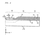
- the confined optical radiation is then coupled to adjacent InGaAsP passive straight branch waveguide 240 (1.1 ⁇ m bandgap layer), extending from and underlying active InGaAsP layer 130, as shown in FIG. 2 illustrating the cross sectional thereof. It should be noted that active InGaAsP layer 130 is removed from passive waveguide areas.
- Straight branch waveguide 240 is used as an output port while side branch waveguide 260 extends to and underlies active InGaAsP layer 330 (1.3 ⁇ m bandgap energy layer), optically coupling about 10 % of the incident optical radiation to p-i-n detector 300. Similar to a portion of straight branch waveguide 240 in the active amplifier section, side branch waveguide 260 in a portion of the photodetector section is adjacent to active InGaAsP layer 330 for coupling optical radiation to photodetector 300. It should be noted that the location of buried Y-junction waveguide 200, that is straight and side branch waveguides 260 and 240, are shown projected on the top surface by dotted lines.
- Both side and straight branch waveguide 260 and 240 are passive InGaAsP (1.1 ⁇ m bandgap) waveguide mesas buried by a semi-insulating InP region 120. Angles other than 3.5 ° between the branches may be used for different desired power splitting ratio.
- the power splitting ratio is controlled by the widths W1 and W2 of straight branch waveguide 240 and side branch waveguide 260, respectively, and the angle ⁇ between the branches.
- the width W2 should be narrower than the width W1.
- the angle may be chosen in accordance with the desired power division and is, generally, limited to a few degrees because of fabrication limitations and bending loss considerations.
- junction region 280 a gradual change in the effective refractive index along the Z-axis in junction region 280 between side branch 260 and straight branch 240 is employed to reduce the effect of the wedge truncation seen by optical radiation egressing from optical amplifier 100.
- the refractive effective index of junction region 280 has a linear gradient index profile along the Z-axis, varying from the core index to the cladding index of straight and side branch waveguides 240 and 260, respectively.
- Other profiles may, however, be employed such as a parabolic, exponential or step function profile. It is contemplated that in the preferred embodiment, both side and straight branch waveguides are single mode waveguides.
- a semi-insulating blocked planar buried heterostructure (SIPBH) waveguide with an active InGaAsP layer (1.3 ⁇ m bandgap energy) structure is employed for both optical amplifier 100 and p-i-n photodetector 300.
- a Fe doped semi-insulating InP region 120 is used for both current blocking and transverse optical confinement in optical amplifier 100 and photodetector 300.
- the active layer is removed for passive Y-junction waveguide 200 and, thus, optical amplifier 100 and photodetector 300 are similar to Y-junction waveguide 200 except for active InGaAsP layers 130, 330 and p conducrivity type layers 150, 350, which facilitate electrical contact to the respective active InGaAsP layers.
- junction region 280 between the branches of the Y-junction has a gradual change in the effective refractive index along the Z-axis, as discussed aboveherein, to reduce the effect of the wedge tip truncation seen by an optical mode propagating therein from optical amplifier 100. This may be accomplished, as is the case here, by a gradual decrease along the Z-axis in thickness of an InGaAsP region in Y-junction region 280 underlying InP region 120.
- Semi-insulating InP region 120 is also used for a top passive cladding waveguide region because it has a smaller absorption loss coefficient than p conductivity type layers 150, 350.
- passive InGaAsP straight and side waveguides 240 and 260, respectively, and active InGaAsP layers 130, 330 have respective thickness of 0.35 ⁇ m and 0.9 ⁇ m.
- the widths of both the active and passive waveguides outside Y-junction area 290 are 2.5 ⁇ m.
- FIGs. 3 a top plan view of Y-junction waveguide 200 is illustrated.
- the direction from straight waveguide 240 toward side waveguide 260 is taken as the Z-axis and the direction perpendicular to the plane of the drawing is taken as the Y-axis in order to define a X-Y-Z coordinate system, as shown in FIG. 3.
- the 2.5 ⁇ m width W of the straight branch waveguide 240 is tapered by a 80 ⁇ m tapering length for adiabatic mode propagation into Y-junction area 290. Power division occurs by mode conversion at the Y-junction, with the modal behavior dominated by the abrupt transition at the truncated wedge tip 210.
- the widths of the waveguides at junction tip 210 are 2.2 ⁇ m and 3.3 ⁇ m for side branch waveguide 260 and straight branch waveguide 240, respectively. Further, the width of truncated wedge rip 210 is 0.8 ⁇ m. In this exemplary structure, the widths of both waveguides are tapered back to a width W of 2.5 ⁇ m at about 100 ⁇ m outside of the Y-junction tip, as shown in FIG. 3.
- optical amplifier 100, p-i-n photodetector 300 and Y-junction waveguide 200 is realized by three epitaxial growth steps and by conventional photolithography and wet chemical etching. That is, a planar metal-organic chemical vapor deposition (MOCVD) growth for InGaAsP active layers 130, 330 and InGaAsP passive waveguide layers 240, 260 followed by two MOCVD regrowths for blocking layers 120 and cap layers 150, 350.
- MOCVD metal-organic chemical vapor deposition
- active layers 130, 330 and passive waveguide layer 240, 260 are grown on n-type InP substrate 160, 2-3 ⁇ m wide mesas are etched using a SiO2 mask in order to form active regions 130 and 330, and straight branch region 240 and side branch waveguide 260.
- Y-junction waveguide mesas and the active waveguide mesas are etched using a SiO2 mask with the straight sections parallel to the [011] orientation.
- passive Y-junction waveguide 200 will be similar to the active section, that is optical amplifier 100 and photodetector 300, except for active layer 130, 330 and cap layers 150, 350.
- the total height of the active waveguide mesas are 1.5 -2 ⁇ m, and the height of the Y-junction mesa is less than 1 ⁇ m.
- a MOCVD regrowth is performed for forming semi-insulating block InP region 120.
- the active waveguide is completely planarized with semi-insulating InP region 120, while the passive Y-branch is covered thereby.
- the SiO2 mask is removed and cap layers 150, 350 grown by MOCVD over active regions 130 and 330 of optical amplifier 100 and photodetector 300, respectively.
- Cap layers 150, 350 consist of a 1.5 ⁇ m p-InP layer followed by a 0.5 ⁇ m p+ InGaAs layer.
- the processing steps are different than conventional photolithographic steps.
- the passive InGaAsP between side branch waveguide 260 and straight branch waveguide 240 is only partially removed by a shallow etch when defining waveguide mesas 240 and 260, as discussed above.
- a second deep etch produces the passive InGaAsP waveguide mesas.
- the thickness of the shallow etched InGaAsP layer which remains between the two branches is 0.2 ⁇ m and tapers to zero over a length of 100 ⁇ m from Y-junction tip 210.
- the regrowth of semi-insulating InP region 120 over the InGaAsP layer buries the passive waveguides, giving the effective refracrive index shown in FIGs. 4 through 8.
- Active layers 130, 330 are subsequently covered by a third MOCVD growth of the p-InP and p InGaAs contact layers as discussed above. These layers in the passive waveguide and Y-junction areas are subsequently removed by chemical etching.
- All the etching steps above are done using standard selective etchants, such as a 2:1 mixture of HCl:H3PO4 for InP and a 3:1:1 mixture of H2SO 4: H2O2:H2O for InGaAsP and InGaAs.
- standard selective etchants such as a 2:1 mixture of HCl:H3PO4 for InP and a 3:1:1 mixture of H2SO 4: H2O2:H2O for InGaAsP and InGaAs.
- optical amplifier 100 is formed by depositing antireflective coatings on the end facets.
- optical amplifier 100 may be made into a laser either by integrating a grating in order to provide distributed feedback or by utilizing the Fabry-Perot resonances from the end facets, if made to have a sufficiently high reflectivity. See, for example, K.Y Liou et al., Appl. Phys. Lett. Vol. 54 No. 2 pp. 114-6 (1989).
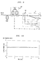
- FIG. 9 illustrates a schematic of an external feedback circuit that was added to integrated structure 10 to permit the output power to be automatically maintained constant over a specified range of input power levels and polarization.
- Feedback circuit 500 compares the current from photodetector 300 with a reference value at differential amplifier 510 that adjusts the bias current to optical amplifier 100. Shown in FIG. 10 is the recorded trace of the amplifier output power as stablized by feedback circuit 500. It should be noted that a constant output power of 3.5 mW is demonstrated with the input power (> 30 ⁇ W) allowed to vary and the input polarization allowed to rotate about +/- 25 °.
- a fiber polarization controller 520 may be utilized to optimize the optical gain by maximizing current from photodetector 300. That is, polarization controller 520 may be operated electrically via feedback circuit 500 such that the peak photocurrent can be used to automatically maintain maximum amplifier gain.
- optical amplifier 100 Before anti-reflective coating the end facets of the structure of FIG. 1, optical amplifier 100 operates as composite-cavity laser, having approximately a threshold current of 80 mA at 22 ° C.
- FIG. 11 illustrates the typical photocurrent generated by unbiased photodetector 300 as a function of the amplifier bias current I b before and after anti-reflective coating an output facet of integrated structure 10. By coating both facets, a traveling wave amplifier is formed. With an injected current of 130 mA into optical amplifier 100, the spontaneous emission spectrum exhibits ripples of ⁇ 0.4 dB due to residual Fabry-Perot resonances, with mode separation of 0.9 ⁇ .
- the above described invention is not limited to an optical amplifier, but can be also be used with other devices. Regardless of the specific device use, it is important to be able to monitor and control the output power of the device.
- device structures that incorporate a detector on the same chip as an optical amplifier or the like are important because such integrated devices can provide the full benefits which result from integration, such as compactness, reliability, low cost, and high performance.
- the ability to monolithically integrate a photodetector with an optical amplifier affords an in-situ anti-reflection coating technique.
- the coating material may be applied to an exposed facet while the amplifier is biased.
- the optimum anti-reflective coating thickness is determined when the photo-generated current from monitoring detector 300 reaches a minimum, for a specific bias current, according to the graph shown in FIG. 11. Note that if a high reflective coating is desired, such as for lasing, the coating thickness may be optimized by maximizing the photocurrent from photodetector 300.
- Illustrated in Fig. 12 is the variation of the amplified output power with rotation of the input polarization. Electrically controlling the polarizer in a feedback configuration by the photocurrent realizes a polarization feedback loop which operates automatically to maintain a maximum amplifier gain if the photocurrent is maximized. Additionally, as illustrated by FIG. 12, the photocurrent generated is highly dependent on the polarization of the ingressing optical radiation. Thus, it is possible to measure the degree of polarization by correlating the photocurrent to the state of polarization vis-a-viS FIG. 12. That is, a polarization detector can be realized by utilizing the device of FIG. 1 and measuring the generated photocurrent. Of course, this assumes that the measured photocurrents are normalized.
Landscapes
- Physics & Mathematics (AREA)
- General Physics & Mathematics (AREA)
- Optics & Photonics (AREA)
- Condensed Matter Physics & Semiconductors (AREA)
- Electromagnetism (AREA)
- Engineering & Computer Science (AREA)
- Microelectronics & Electronic Packaging (AREA)
- Semiconductor Lasers (AREA)
- Solid State Image Pick-Up Elements (AREA)
- Light Receiving Elements (AREA)
- Photometry And Measurement Of Optical Pulse Characteristics (AREA)
- Optical Integrated Circuits (AREA)
Applications Claiming Priority (2)
| Application Number | Priority Date | Filing Date | Title |
|---|---|---|---|
| US07/563,164 US5134671A (en) | 1990-08-03 | 1990-08-03 | Monolithic integrated optical amplifier and photodetector |
| US563164 | 1990-08-03 |
Publications (2)
| Publication Number | Publication Date |
|---|---|
| EP0469793A2 true EP0469793A2 (de) | 1992-02-05 |
| EP0469793A3 EP0469793A3 (en) | 1992-12-23 |
Family
ID=24249359
Family Applications (1)
| Application Number | Title | Priority Date | Filing Date |
|---|---|---|---|
| EP19910306814 Withdrawn EP0469793A3 (en) | 1990-08-03 | 1991-07-25 | Monolithic integrated optical amplifier and photodetector |
Country Status (4)
| Country | Link |
|---|---|
| US (1) | US5134671A (de) |
| EP (1) | EP0469793A3 (de) |
| JP (1) | JPH04254380A (de) |
| CA (1) | CA2041706C (de) |
Cited By (7)
| Publication number | Priority date | Publication date | Assignee | Title |
|---|---|---|---|---|
| EP0593237A3 (de) * | 1992-10-13 | 1994-05-04 | Nec Corporation | Optischer Halbleiterverstärker |
| EP0687926A1 (de) | 1994-06-17 | 1995-12-20 | Koninklijke KPN N.V. | Optischer Leistungsteilerschaltkreis unabhängig von der Polarisation und Wellenlänge |
| NL1008206C2 (nl) * | 1998-02-05 | 1999-08-06 | Koninkl Kpn Nv | Optisch circuit voor het verkrijgen van een monitorsignaal voor het bewaken van een optische schakelaar. |
| EP1115012A1 (de) * | 2000-01-06 | 2001-07-11 | Corning Incorporated | Wellenleiter mit vertiefter Anzapfstelle für die optische Überwachung von optischen Bauelementen |
| EP0867984A3 (de) * | 1997-03-28 | 2004-01-14 | Lucent Technologies Inc. | Herstellung von integrierten photonischen Schaltkreisen |
| WO2012041850A1 (en) * | 2010-09-30 | 2012-04-05 | Alcatel Lucent | A monolithic integrated structure comprising a buried heterostructure semiconductor optical amplifier and a photodetector |
| EP3714299A4 (de) * | 2019-01-23 | 2021-10-06 | Nexus Photonics LLC | Integrierte aktive vorrichtungen mit verbesserter optischer kopplung mit dielektrischen wellenleitern |
Families Citing this family (39)
| Publication number | Priority date | Publication date | Assignee | Title |
|---|---|---|---|---|
| SE468267B (sv) * | 1991-04-10 | 1992-11-30 | Ericsson Telefon Ab L M | Terminal foer ett frekvensdelat, optiskt kommunikationssystem |
| US5523879A (en) * | 1991-04-26 | 1996-06-04 | Fuji Xerox Co., Ltd. | Optical link amplifier and a wavelength multiplex laser oscillator |
| JPH04372907A (ja) * | 1991-06-21 | 1992-12-25 | Canon Inc | 導波型分岐、結合素子 |
| US5253314A (en) * | 1992-01-31 | 1993-10-12 | At&T Bell Laboratories | Tunable optical waveguide coupler |
| FR2694099B1 (fr) * | 1992-07-21 | 1994-12-09 | Louis Menigaux | Procédé pour former une structure à guide de lumière et miroir intégrés, et structure ainsi réalisée. |
| US5228103A (en) * | 1992-08-17 | 1993-07-13 | University Of Maryland | Monolithically integrated wavelength division multiplexing laser array |
| DE4304993A1 (de) * | 1993-02-18 | 1994-08-25 | Sel Alcatel Ag | Verfahren zur Herstellung eines kaskadierten optischen Raumschalters und nach diesem Verfahren hergestellter kaskadierter optischer Raumschalter |
| SE503905C2 (sv) * | 1994-03-16 | 1996-09-30 | Ericsson Telefon Ab L M | Förfarande för framställning av en optokomponent samt optokomponent |
| US5457569A (en) * | 1994-06-30 | 1995-10-10 | At&T Ipm Corp. | Semiconductor amplifier or laser having integrated lens |
| JP3258542B2 (ja) * | 1995-07-12 | 2002-02-18 | 日本電信電話株式会社 | 分岐合流光導波路 |
| US5577139A (en) * | 1995-08-17 | 1996-11-19 | Lucent Technologies Inc. | Integrated-circuit optical network unit |
| US5577138A (en) * | 1995-08-17 | 1996-11-19 | Lucent Technologies Inc. | Integrated-circuit optical network unit |
| US6078707A (en) * | 1995-09-22 | 2000-06-20 | Sharp Kabushiki Kaisha | Waveguide-photodetector, method for producing the same, waveguide usable in the waveguide-photodetector, and method for producing the same |
| US5812582A (en) * | 1995-10-03 | 1998-09-22 | Methode Electronics, Inc. | Vertical cavity surface emitting laser feedback system and method |
| JPH09153638A (ja) * | 1995-11-30 | 1997-06-10 | Nec Corp | 導波路型半導体受光装置およびその製造方法 |
| DE19605794A1 (de) * | 1996-02-16 | 1997-08-21 | Sel Alcatel Ag | Monolithisch integriertes optisches oder optoelektronisches Halbleiterbauelement und Herstellungsverfahren |
| US6275317B1 (en) | 1998-03-10 | 2001-08-14 | Agere Systems Optoelectronics Guardian Corp. | Hybrid integration of a wavelength selectable laser source and optical amplifier/modulator |
| EP1130718A3 (de) * | 2000-01-20 | 2003-07-02 | Cyoptics (Israel) Ltd. | Stabilisierter frequenzverstimmbarer Laser mit Fasergitter |
| US6417528B1 (en) | 2000-01-28 | 2002-07-09 | Agere Systems Guardian Corp. | High speed semiconductor photodetector |
| US6453105B1 (en) | 2000-10-04 | 2002-09-17 | Agere Systems Guardian Corp | Optoelectronic device with power monitoring tap |
| CA2463278C (en) * | 2001-10-09 | 2013-04-02 | Infinera Corporation | Transmitter photonic integrated circuits (txpic) and optical transport networks employing txpics |
| US20030133663A1 (en) * | 2002-01-16 | 2003-07-17 | Jds Uniphase Corporation | Integrated optical splitter |
| GB2387481B (en) * | 2002-04-10 | 2005-08-31 | Intense Photonics Ltd | Integrated active photonic device and photodetector |
| KR100617693B1 (ko) * | 2003-08-20 | 2006-08-28 | 삼성전자주식회사 | 광검출기를 구비하는 반도체 광증폭 장치 및 그 제조방법 |
| US7272273B2 (en) * | 2005-01-21 | 2007-09-18 | Neophotonics Corporation | Photodetector coupled to a planar waveguide |
| JP4632841B2 (ja) * | 2005-03-31 | 2011-02-16 | 富士通株式会社 | 半導体デバイス |
| US7343061B2 (en) * | 2005-11-15 | 2008-03-11 | The Trustees Of Princeton University | Integrated photonic amplifier and detector |
| US7826693B2 (en) * | 2006-10-26 | 2010-11-02 | The Trustees Of Princeton University | Monolithically integrated reconfigurable optical add-drop multiplexer |
| KR20120070836A (ko) * | 2010-12-22 | 2012-07-02 | 한국전자통신연구원 | 다파장 광 발생 장치 |
| JP5742344B2 (ja) | 2011-03-20 | 2015-07-01 | 富士通株式会社 | 受光素子、光受信器及び光受信モジュール |
| KR102351574B1 (ko) * | 2015-04-30 | 2022-01-14 | 한국전자통신연구원 | 포토 다이오드 |
| US11211768B2 (en) * | 2017-10-03 | 2021-12-28 | Mitsubishi Electric Corporation | Semiconductor optical integrated device |
| JP6758546B1 (ja) * | 2020-01-16 | 2020-09-23 | 三菱電機株式会社 | 半導体光集積素子およびその製造方法 |
| US11204463B1 (en) * | 2020-07-17 | 2021-12-21 | Globalfoundries U.S. Inc. | Integrated circuit structure with optical absorber layer over optical grating coupler |
| CN114361749B (zh) * | 2022-01-26 | 2022-08-30 | 清华大学 | 一种具有片上集成偏置器的毫米波光电混频器件 |
| CN116053923A (zh) * | 2022-12-30 | 2023-05-02 | 中国科学院苏州纳米技术与纳米仿生研究所 | 集成式半导体激光器闭环控制装置 |
| CN119674696A (zh) * | 2024-12-09 | 2025-03-21 | 无锡华兴光电研究有限公司 | 一种自带功率监测的半导体激光器 |
| CN120566223B (zh) * | 2025-07-28 | 2026-03-13 | 陕西源杰半导体科技股份有限公司 | 集成分支波导和光电二极管的半导体器件 |
| CN120869344B (zh) * | 2025-09-26 | 2026-02-17 | 中南大学 | 应用于硅光波导的非侵入式光功率监测结构与监测方法 |
Family Cites Families (4)
| Publication number | Priority date | Publication date | Assignee | Title |
|---|---|---|---|---|
| US4674827A (en) * | 1982-05-20 | 1987-06-23 | Masayuki Izutsu | Slab-type optical device |
| DE3687162D1 (de) * | 1985-12-10 | 1993-01-07 | Siemens Ag | Integriert-optischer multiplex-demultiplex-modul fuer die optische nachrichtenuebertragung. |
| US4846540A (en) * | 1988-01-25 | 1989-07-11 | Bell Communications Research, Inc. | Optical wavegide junction |
| US4878727A (en) * | 1988-06-30 | 1989-11-07 | Battelle Memorial Institute | Multimode channel waveguide optical coupling devices and methods |
-
1990
- 1990-08-03 US US07/563,164 patent/US5134671A/en not_active Expired - Lifetime
-
1991
- 1991-05-02 CA CA002041706A patent/CA2041706C/en not_active Expired - Lifetime
- 1991-07-25 EP EP19910306814 patent/EP0469793A3/en not_active Withdrawn
- 1991-07-31 JP JP3190423A patent/JPH04254380A/ja active Pending
Non-Patent Citations (3)
| Title |
|---|
| APPLIED PHYSICS LETTERS vol. 54, no. 2, 9 January 1989, NEW YORK US pages 114 - 116 LIOU ET AL 'Monolithic integrated InGaAsP/InP distributed feedback laser with Y-branching waveguide and a monitoring photodetector grown by metalorganic chemical vapor deposition' * |
| CONFERENCE ON LASERS AND ELECTRO-OPTICS vol. 7, May 1990, ANAHEIM, US pages 494 - 495 LIOU ET AL 'Monolithically integrated GaInAsP/InP optical amplifier with low loss Y-branching waveguides and monitoring photodetector' * |
| OPTICAL FIBER COMMUNICATION CONFERENCE vol. 1, January 1990, SAN FRANCISCO US page 183 LIOU ET AL 'Asymmetric optical waveguide Y-junction in InGaAsP/InP photonic integrated circuits' * |
Cited By (13)
| Publication number | Priority date | Publication date | Assignee | Title |
|---|---|---|---|---|
| US5414554A (en) * | 1992-10-13 | 1995-05-09 | Nec Corporation | Optical semiconductor amplifier |
| EP0593237A3 (de) * | 1992-10-13 | 1994-05-04 | Nec Corporation | Optischer Halbleiterverstärker |
| EP0687926A1 (de) | 1994-06-17 | 1995-12-20 | Koninklijke KPN N.V. | Optischer Leistungsteilerschaltkreis unabhängig von der Polarisation und Wellenlänge |
| US5524156A (en) * | 1994-06-17 | 1996-06-04 | Koninklijke Ptt Nederland N.V. | Polarization and wavelength independent optical power splitting circuit |
| EP0867984A3 (de) * | 1997-03-28 | 2004-01-14 | Lucent Technologies Inc. | Herstellung von integrierten photonischen Schaltkreisen |
| NL1008206C2 (nl) * | 1998-02-05 | 1999-08-06 | Koninkl Kpn Nv | Optisch circuit voor het verkrijgen van een monitorsignaal voor het bewaken van een optische schakelaar. |
| WO1999040738A1 (en) * | 1998-02-05 | 1999-08-12 | Koninklijke Kpn N.V. | Optical circuit for obtaining a monitor signal |
| AU745931B2 (en) * | 1998-02-05 | 2002-04-11 | Koninklijke Kpn N.V. | Optical circuit for obtaining a monitor signal |
| EP1115012A1 (de) * | 2000-01-06 | 2001-07-11 | Corning Incorporated | Wellenleiter mit vertiefter Anzapfstelle für die optische Überwachung von optischen Bauelementen |
| WO2012041850A1 (en) * | 2010-09-30 | 2012-04-05 | Alcatel Lucent | A monolithic integrated structure comprising a buried heterostructure semiconductor optical amplifier and a photodetector |
| EP2439822A1 (de) * | 2010-09-30 | 2012-04-11 | Alcatel Lucent | Monolithische integrierte Anordnung mit einem optischen Halbleiterverstärker der eine vergrabene Heterostruktur enthält und einem Photodetektor |
| US8995804B2 (en) | 2010-09-30 | 2015-03-31 | Alcatel Lucent | Monolithic integrated structure comprising a buried heterostructure semiconductor optical amplifier and a photodetector |
| EP3714299A4 (de) * | 2019-01-23 | 2021-10-06 | Nexus Photonics LLC | Integrierte aktive vorrichtungen mit verbesserter optischer kopplung mit dielektrischen wellenleitern |
Also Published As
| Publication number | Publication date |
|---|---|
| US5134671A (en) | 1992-07-28 |
| CA2041706A1 (en) | 1992-02-04 |
| CA2041706C (en) | 1998-07-07 |
| JPH04254380A (ja) | 1992-09-09 |
| EP0469793A3 (en) | 1992-12-23 |
Similar Documents
| Publication | Publication Date | Title |
|---|---|---|
| US5134671A (en) | Monolithic integrated optical amplifier and photodetector | |
| US5127081A (en) | Optical branching waveguide | |
| EP1297369B1 (de) | Photonischer integrierter detektor mit mehreren asymmetrischen wellenleitern | |
| US5457569A (en) | Semiconductor amplifier or laser having integrated lens | |
| US5703989A (en) | Single-mode waveguide structure for optoelectronic integrated circuits and method of making same | |
| EP1254385B1 (de) | Verbesserte integrierte optische vorrichtung | |
| EP0725287B1 (de) | Integriertes optisches Regelelement und Verfahren zu seiner Herstellung und integriertoptisches Element und es verwendende integriertoptische Schaltkreisanordnung | |
| EP0898346B1 (de) | Halbleiterlaser mit 1XN vielfachmodigem Interferometer und Emission einer transversaler Mode | |
| JP4117854B2 (ja) | 導波路型光集積回路素子及びその製造方法 | |
| US5396365A (en) | Polarization-independent optical device and method for polarization-independent processing of a signal | |
| US5029297A (en) | Optical amplifier-photodetector device | |
| CA2165711C (en) | Semiconductor light source having a spectrally broad, high power optical output | |
| US20010021299A1 (en) | Semiconductor waveguide photodetector | |
| Moerman et al. | III–V semiconductor waveguiding devices using adiabatic tapers | |
| Burton et al. | Monolithic InGaAsP-InP laser amplifier gate switch matrix | |
| JP3084417B2 (ja) | 光結合デバイス | |
| SASAKI et al. | In-plane bandgap energy controlled selective MOVPE and its applications to photonic integrated circuits | |
| US5069561A (en) | Monolithically integrated ridge waveguide semiconductor optical preamplifier | |
| KR100433298B1 (ko) | 스폿 사이즈 변환기가 집적된 반도체 광 증폭기의 제조 방법 | |
| Tsuji et al. | High-gain, polarization-independent semiconductor optical amplifier with a large optical cavity and angled buried facets | |
| WO1991003760A1 (en) | Optically coupled waveguides | |
| Liou et al. | Monolithically Integrated 1.5 μm DFB Laser with Y-Branching Waveguide and a Monitoring Photodetector | |
| JPH11112073A (ja) | 半導体レーザ形光増幅素子 | |
| Oh et al. | Optical devices integrated with semiconductor optical amplifier |
Legal Events
| Date | Code | Title | Description |
|---|---|---|---|
| PUAI | Public reference made under article 153(3) epc to a published international application that has entered the european phase |
Free format text: ORIGINAL CODE: 0009012 |
|
| AK | Designated contracting states |
Kind code of ref document: A2 Designated state(s): DE DK FR GB NL |
|
| PUAL | Search report despatched |
Free format text: ORIGINAL CODE: 0009013 |
|
| AK | Designated contracting states |
Kind code of ref document: A3 Designated state(s): DE DK FR GB NL |
|
| 17P | Request for examination filed |
Effective date: 19930610 |
|
| 17Q | First examination report despatched |
Effective date: 19940216 |
|
| RAP3 | Party data changed (applicant data changed or rights of an application transferred) |
Owner name: AT&T CORP. |
|
| STAA | Information on the status of an ep patent application or granted ep patent |
Free format text: STATUS: THE APPLICATION IS DEEMED TO BE WITHDRAWN |
|
| 18D | Application deemed to be withdrawn |
Effective date: 19940628 |