EP0426271A2 - Tragbare Halbleiterspeicheranordnung - Google Patents
Tragbare Halbleiterspeicheranordnung Download PDFInfo
- Publication number
- EP0426271A2 EP0426271A2 EP90304513A EP90304513A EP0426271A2 EP 0426271 A2 EP0426271 A2 EP 0426271A2 EP 90304513 A EP90304513 A EP 90304513A EP 90304513 A EP90304513 A EP 90304513A EP 0426271 A2 EP0426271 A2 EP 0426271A2
- Authority
- EP
- European Patent Office
- Prior art keywords
- cell
- main
- main cell
- storage device
- power
- Prior art date
- Legal status (The legal status is an assumption and is not a legal conclusion. Google has not performed a legal analysis and makes no representation as to the accuracy of the status listed.)
- Granted
Links
Images




Classifications
-
- G—PHYSICS
- G11—INFORMATION STORAGE
- G11C—STATIC STORES
- G11C5/00—Details of stores covered by group G11C11/00
- G11C5/14—Power supply arrangements, e.g. power down, chip selection or deselection, layout of wirings or power grids, or multiple supply levels
- G11C5/141—Battery and back-up supplies
Definitions
- the present invention relates to a portable semiconductor storage device and particularly it relates to a semiconductor storage device capable of replacing a cell provided in it to hold stored data safely and easily.
- a conventional portable semiconductor storage device has such a configuration as that shown in Figure 9.
- the storage device has a static RAM 1, a cell 3 connected to the RAM 1 via an internal power-supply line 9 for supplying a power-supply voltage, a diode 5 for preventing reverse charging and a current limiting resistor 4.
- the cell 3 is held in a cell holder 3a which is removably provided in this storage device.
- the cell 3 is arranged to be electrically connected by stationary electrode terminals 6 and 7 when the cell holder 3a is inserted into the storage device.
- a power-supply input line 8 is connected to the internal power-supply line 9 via a power-supply control circuit 2.
- the power-supply input line 8 is connected to a connector 10.
- An interface bus 11 and a cell monitor output line 12 are connected to the connector 10 from the RAM 1 and the stationary electrode terminal 6 on the positive electrode of the cell 3 respectively.
- the section between the power-supply circuit 2 and the RAM 1 is connected by a control line 13.
- a storage device thus configured is mounted on a terminal equipment (not shown) via the connector 10 when in use. If a power-supply voltage above a prescribed value is applied to the power-supply input line 8, the power-supply control circuit 2 causes this power-supply input line 8 and the internal power-supply line 9 to be conducted and sends out a high-level control signal to the RAM 1 via the control line 13. As a result, a power-supply voltage is supplied to the RAM 1 via the internal power-supply line 9. The RAM 1 is brought into an enable (operable) state by the high-level control signal. That is, the terminal equipment can make an access to the RAM 1, for example, reading from or writing into the RAM 1 via the interface bus 11.
- the power-supply control circuit 2 When access to the RAM 1 is complete and a predetermined power-supply voltage is no longer applied to the power-supply input line 8, the power-supply control circuit 2 detects that the voltage value of the power-supply input line 8 has fallen below the prescribed value. The power-supply control circuit 2 shuts off the section between the power-supply input line 8 and the internal power-supply line 9, and sends out a low-level control signal to the RAM 1 via the control line 13. The RAM 1 is brought into a disable (non-operable) state by this signal, and an access to it by the interface bus 11 is prohibited.
- the power supply voltage from the power-supply input line 8 is not supplied to the RAM 1, but the voltage of the cell 3 is supplied to it via the resistor 4 and the diode 5. Therefore, if this storage device is removed from the terminal equipment, the stored data within the RAM 1 is not erased but held.
- the cell 3 is gradually used up by supplying a voltage to the RAM 1.
- the voltage of the cell 3 is checked by the terminal equipment via the cell monitor output line 12 when the storage device is mounted on the terminal equipment.
- the terminal voltage of the cell 3 falls below a predetermined voltage and the replacement of the cell 3 becomes necessary, the cell 3 can be removed from the storage device together with the cell holder 3a and replaced with a new one.
- FIG. 10 One example of the cell holder 3a is shown in Figure 10.
- a projection 3b is formed on a side of the cell holder 3a.
- the projection 3b of the cell holder 3a is fitted into a recessed portion 15 formed on a frame 14 of the storage device, and the cell holder 3a is fixed.
- the stationary electrode terminals 6 and 7 contact the positive and negative electrodes of the held cell 3 respectively.
- reference numeral 16 indicates a printed circuit board, on which is formed each of the circuit elements shown in Figure 9.
- An object of the present invention is to provide a portable semiconductor storage device capable of replacing a built-in cell safely and easily without erasing stored data.
- the portable semiconductor storage device of the present invention has a device main body, a storage circuit for storing data, a main cell for supplying a power supply voltage to the storage circuit, a main cell holder removably provided in the device main body to hold the main cell, an auxiliary cell for supplying a power-supply voltage to the storage circuit at the time of replacement of the main cell, switch means for operating mechanically by linking with the mounting and removing operation of the main cell holder, to electrically shut off the auxiliary cell from the storage circuit when the main cell holder is mounted in the device main body and electrically connect the auxiliary cell to the storage device when the main cell holder is removed from the device main body.
- the storage device has a static RAM 21.
- An internal power supply line 29 for supplying a power-supply voltage is connected to the RAM 21.
- a main cell 23 is connected to the internal power supply line 29 via a first reverse charging prevention diode 25 and a first current limiting resistor 24.
- the main cell 23 is held in a main cell holder 23a removably provided in this storage device.
- the main cell 23 is electrically connected to stationary electrode terminals 26 and 27.
- an auxiliary cell 37 is connected to the internal power supply line 29 via a second reverse charging prevention diode 35, a second current limiting resistor 34 and switch means 36.
- the switch means 36 is operated by mechanically linking with the mounting and removing operation of the main cell holder 23a. It is opened when the main cell holder 23a is mounted in the device main body (not shown) to connect the main cell 23 between the stationary electrode terminals 26 and 27, while it is short-circuited when the main cell holder 23a is removed form the device main body.
- a power-supply input line 28 is connected to the internal power supply line 29 via a power-supply control circuit 22, and the power-supply input line 28 is connected to a connector 30.
- An interface bus 31 and a cell monitor output line 32 are connected to the connector 30 from the RAM 21 and the stationary electrode terminal 26 on the positive polarity side of the main cell 23 respectively.
- the section between the power-supply control circuit 22 and the RAM 21 is connected by a control line 33.
- the storage device shown in Figure 1 is mounted on a terminal equipment (not shown) via the connector 30 when in use.
- the power-supply control circuit 22 detects this, conducts the power-supply input line 28 and the internal power-supply line 29, and sends out a high-level control signal to the RAM 21 via the control line 33.
- the RAM 21 is supplied with a power-supply voltage via the internal power-supply line 29, and is brought into an enable state by the high-level control signal. That is, the terminal equipment can make an access to the RAM 21, for example, reading from and writing into the RAM 21 via the interface bus 31.
- the power-supply control circuit 22 detects that the voltage value of the power-supply input line 28 has fallen below the prescribed value.
- the power-supply control circuit 22 shuts off the section between the power-supply input line 28 and the internal power-supply line 29, and sends out a low-level control signal to the RAM 21 via the control line 33.
- the RAM 21 is brought into a disable state by this signal, and any access to it is prohibited.
- the power-supply voltage from the power-supply input line 28 is not supplied to the RAM 21, but the voltage of the main cell 23 is supplied to it via the resistor 24 and the diode 25. Therefore, if this storage device is removed from the terminal equipment, the stored data within the RAM 21 is not erased, instead it is held.
- the main cell 23 which holds stored data of the storage device thus removed from the terminal equipment is gradually used up by supplying voltage to the RAM 21.
- the voltage of the main cell 23 is checked by the terminal equipment via the cell monitor output line 32 when the storage device is mounted on the terminal equipment.
- the terminal voltage of the cell 23 falls below a predetermined voltage and the replacement of the main cell 23 becomes necessary, the main cell 23 is removed from the device main body together with the main cell holder 23a and replaced with a new one.
- the switch means 36 is operated by being linked with the removal operation of the main cell holder 23a.
- the auxiliary cell 37 and the second current limiting resistor 34 are connected with each other, and a voltage is supplied to the RAM 21 from the auxiliary cell 37 via switch means 36, the resistor 34 and the diode 35. Therefore, if the main cell 23 is removed from the storage device together with the main cell holder 23a under the condition that the storage device is not mounted on the terminal equipment, the stored data within the RAM 21 is held without being erased.
- the switch means 36 is opened by being linked with the insertion operation of the main cell holder 23a. Therefore, the auxiliary cell 37 is separated from the RAM 21, and instead the new main cell 23 supplies a voltage to the RAM 21 via the resistor 24 and the diode 25.
- the main cell 23 can easily be replaced while the stored data is held under the condition that the storage device is not mounted on the terminal equipment but in a portable state.
- a predetermined timing is required between the mounting and removing operation of the main cell holder 23a and the operation of the switch means 36 which operates by linking with the operation of the main cell holder 23a. That is, as shown in Figure 2, when the main cell holder 23a is removed, it is required that at time to before time t1 when the main cell 23 is separated from the stationary electrode terminals 26 and 27, the switch means 36 is short-cicuited, causing the auxiliary cell 37 to be connected to the RAM 21.
- the switch means 36 is opened and the auxiliary cell 37 is shut off from the RAM 21.
- the time period must be set by considering the chatterings C1 and C2 of each contact. As shown in Figure 2, even if the chatterings C1 and C2 are eliminated, the timing should preferably have time T1 and T2 if both the main cell 23 and the auxiliary cell 37 are to be reliably connected to the RAM 21.
- a printed circuit board 39 is fixed within a frame 38 constituting a device main body.
- a notch 39a is formed on one corner of this printed circuit board 39, and the main cell holder 23a is inserted in the frame 38 in this portion.
- the stationary electrode terminals 26 and 27, each of which has one end fixed to the printed circuit board 39, are placed within the notch 39a of the printed circuit board 39, and contact the positive and negative polarities of the main cell 23 held in the main cell holder 23a respectively.
- a rotary slide switch 40 is formed on a portion of the printed circuit board 39 facing the notch 39a.
- This rotary slide switch 40 includes a movable contact 42 rotatably provided around a fulcrum 41 and a pair of fixed contacts 43 and 44 fixed on the printed circuit board 39.
- the auxiliary cell 37 is placed in the vicinity of the rotary slide switch 40.
- the auxiliary cell 37 is attached with tabs 45 and 46 which are connected to the positive and negative polarities of the auxiliary cell 37, and the tab 45 on the positive side is connected to the fixed contact 43 of the rotary slide switch 40 by soldering.
- each of the circuit elements shown in Figure 1 is formed on the printed circuit board 39.
- the stationary electrode terminal 27 and the tab 46 on the negative side of the auxiliary cell 37 are connected to the ground line, and the other stationary electrode terminal 26 and the fixed contact 44 of the rotary slide switch 40 are connected to corresponding circuit elements respectively.
- a projection 47 for actuating the rotary slide switch 40 is formed on the main cell holder 23a. For this reason, when the main cell holder 23a is inserted in the frame 38 as shown in Figure 3, the projection 47 of the main cell holder 23a contacts the movable contact 42 of the rotary slide switch 40 and causes the movable contact 42 to be fixed to a position away from the fixed contacts 43 and 44. That is, the rotary slide switch 40 is opened, and the auxiliary cell 37 is electrically shut off from the not-shown RAM.
- the movable contact 42 of the rotary slide switch 40 is made to rotate clockwise by the projection 47 of the main cell holder 23a, and as shown in Figure 4, it is positioned on the fixed contacts 43 and 44, these contacts being electrically short-circuited. That is, the rotary slide switch 40 is turned on, and the auxiliary cell 37 is connected to the not-shown RAM.
- the movable contact 42 and the fixed contacts 43 and 44 are provided on the printed circuit board 39 to form the rotary slide switch 40.
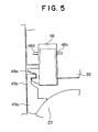
- a rotary slide switch 48 formed of a combination of a movable contact 48a, and fixed contacts 48b and 48c is prepared as a single body in advance and this switch 48 may be mounted on the printed circuit board 39.
- Reference numeral 49b designates a projection formed on a main cell holder 49a holding the main cell 23.
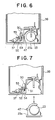
- FIG. 6 shows an essential part of a third embodiment.
- This third embodiment is one such that a push-off switch 50 is used as the switch means 36 instead of the rotary slide switch 40 in the second embodiment.
- the push-off switch 50 has a movable contact 51 which is provided linearly movably, and the fixed contacts 52 and 53 which are positionally fixed, and the movable contact 51 is energized toward the fixed contacts 52 and 53 by a spring 54.
- the projection 47 of the main cell holder 23a causes the movable contact 51 of the push-off switch 50 to move, and to be fixed to a position separated from the fixed contacts 52 and 53, thereby opening the push-off switch 50. That is, the auxiliary cell 37 is electrically shut off from a not-shown RAM.
- the timings of connection and disconnecion for each of the main cell 23 and the auxiliary cell 37 can be set as shown in Figure 2.
- the auxiliary cell 37 with tabs was mounted on the printed circuit board 39.
- an auxiliary cell holder 37a may be removably provided on the frame 38 so as to hold the auxiliary cell 37. Since it is not necessary for this auxiliary cell holder 37a to be linked with switch means, a holder similar to the conventional cell holder 3a shown in Figure 10 can be employed. By using the auxiliary cell holder 37a in this manner, the auxiliary cell 37 can be replaced easily, and furthermore convenience can be improved.
- a switch having a multi-contact structure may be used.
- the main cell 23 and the auxiliary cell 37 can be switched by using one contact and the information regarding the switching of these cells is output to the terminal via the connector 30 by using the other contacts. Therefore, for example, when the auxiliary cell 37 is in use, this can be displayed and an alarm sounded.
- the rotary slide switches 40, 48 and the push-off switch 50 are mounted on both sides of the printed circuit board 39, and these switches may simultaneously be operated by linking with the mounting and removing operation of the main cell holder 23a.
Landscapes
- Engineering & Computer Science (AREA)
- Power Engineering (AREA)
- Battery Mounting, Suspending (AREA)
- Power Sources (AREA)
- Techniques For Improving Reliability Of Storages (AREA)
Applications Claiming Priority (2)
| Application Number | Priority Date | Filing Date | Title |
|---|---|---|---|
| JP1284854A JPH03147116A (ja) | 1989-11-02 | 1989-11-02 | 所持携帯型半導体記憶装置 |
| JP284854/89 | 1989-11-02 |
Publications (3)
| Publication Number | Publication Date |
|---|---|
| EP0426271A2 true EP0426271A2 (de) | 1991-05-08 |
| EP0426271A3 EP0426271A3 (en) | 1992-01-02 |
| EP0426271B1 EP0426271B1 (de) | 1995-09-06 |
Family
ID=17683892
Family Applications (1)
| Application Number | Title | Priority Date | Filing Date |
|---|---|---|---|
| EP90304513A Expired - Lifetime EP0426271B1 (de) | 1989-11-02 | 1990-04-26 | Tragbare Halbleiterspeicheranordnung |
Country Status (4)
| Country | Link |
|---|---|
| US (1) | US5079741A (de) |
| EP (1) | EP0426271B1 (de) |
| JP (1) | JPH03147116A (de) |
| DE (1) | DE69022164T2 (de) |
Cited By (1)
| Publication number | Priority date | Publication date | Assignee | Title |
|---|---|---|---|---|
| EP0762242A1 (de) * | 1995-08-31 | 1997-03-12 | Seiko Epson Corporation | Tragbare elektronische Vorrichtung |
Families Citing this family (11)
| Publication number | Priority date | Publication date | Assignee | Title |
|---|---|---|---|---|
| US5204963A (en) * | 1990-12-07 | 1993-04-20 | Digital Equipment Corporation | Method and apparatus for a backup power controller for volatile random access memory |
| JP2594181B2 (ja) * | 1991-02-04 | 1997-03-26 | シャープ株式会社 | 携帯用電子機器 |
| US5552240A (en) * | 1994-10-25 | 1996-09-03 | The Whitaker Corporation | Battery operated component with removable battery holder |
| JP3222714B2 (ja) * | 1995-01-24 | 2001-10-29 | 松下電器産業株式会社 | 押圧・回転操作型電子部品 |
| US5862071A (en) * | 1996-05-10 | 1999-01-19 | Dell Usa, L.P. | Receptacle for touch memory button |
| US6141223A (en) * | 1998-05-08 | 2000-10-31 | Smk Manufacturing, Inc. | Battery assembly for supplying power to an integrated circuit |
| JP5651457B2 (ja) * | 2010-12-15 | 2015-01-14 | 株式会社東芝 | 半導体記憶装置 |
| JP6395835B2 (ja) | 2014-08-08 | 2018-09-26 | エスゼット ディージェイアイ テクノロジー カンパニー リミテッドSz Dji Technology Co.,Ltd | Uavのバッテリー電源バックアップシステムおよび方法 |
| CN106068592B (zh) | 2014-08-08 | 2021-06-11 | 深圳市大疆创新科技有限公司 | 无人飞行器电池更换系统及方法 |
| JP6390022B2 (ja) | 2014-08-08 | 2018-09-19 | エスゼット ディージェイアイ テクノロジー カンパニー リミテッドSz Dji Technology Co.,Ltd | エネルギー提供ステーション |
| WO2016078093A1 (en) | 2014-11-21 | 2016-05-26 | SZ DJI Technology Co., Ltd. | System and method for managing unmanned aerial vehicles |
Family Cites Families (10)
| Publication number | Priority date | Publication date | Assignee | Title |
|---|---|---|---|---|
| US4255697A (en) * | 1980-01-21 | 1981-03-10 | David Edwards | Cash register power supply system |
| DE3416780A1 (de) * | 1984-05-07 | 1985-11-07 | Siemens AG, 1000 Berlin und 8000 München | Batteriepufferung und batterieueberwachung bei fluechtigen halbleiterspeichern |
| US4662736A (en) * | 1984-12-29 | 1987-05-05 | Minolta Camera Kabushiki Kaisha | Power supply system for memory unit of camera |
| US4607351A (en) * | 1985-01-14 | 1986-08-19 | International Business Machine Corp. | Cartridge memory protection |
| DE8535374U1 (de) * | 1985-12-17 | 1986-03-06 | Fichtel & Sachs Ag, 8720 Schweinfurt | Batteriebetriebene elektronische Einrichtung zur Geschwindigkeits- und Wegmessung, insbesondere für Fahrräder oder dgl. |
| JPH0657477B2 (ja) * | 1987-03-31 | 1994-08-03 | 三菱電機株式会社 | 半導体装置カ−ド |
| JPS6448117A (en) * | 1987-08-19 | 1989-02-22 | Fuji Photo Film Co Ltd | Memory cartridge |
| US4956563A (en) * | 1987-11-09 | 1990-09-11 | Perma Power Electronics, Inc. | Standby power supply |
| JPH01188921A (ja) * | 1988-01-22 | 1989-07-28 | Mitsubishi Electric Corp | メモリカード |
| JPH0769759B2 (ja) * | 1988-09-08 | 1995-07-31 | 三菱電機株式会社 | メモリカード用接続機構 |
-
1989
- 1989-11-02 JP JP1284854A patent/JPH03147116A/ja active Pending
-
1990
- 1990-01-16 US US07/465,500 patent/US5079741A/en not_active Expired - Lifetime
- 1990-04-26 EP EP90304513A patent/EP0426271B1/de not_active Expired - Lifetime
- 1990-04-26 DE DE69022164T patent/DE69022164T2/de not_active Expired - Fee Related
Cited By (2)
| Publication number | Priority date | Publication date | Assignee | Title |
|---|---|---|---|---|
| EP0762242A1 (de) * | 1995-08-31 | 1997-03-12 | Seiko Epson Corporation | Tragbare elektronische Vorrichtung |
| US5787054A (en) * | 1995-08-31 | 1998-07-28 | Seiko Epson Corporation | Portable electronic device |
Also Published As
| Publication number | Publication date |
|---|---|
| DE69022164T2 (de) | 1996-05-09 |
| EP0426271B1 (de) | 1995-09-06 |
| JPH03147116A (ja) | 1991-06-24 |
| EP0426271A3 (en) | 1992-01-02 |
| DE69022164D1 (de) | 1995-10-12 |
| US5079741A (en) | 1992-01-07 |
Similar Documents
| Publication | Publication Date | Title |
|---|---|---|
| JP2594181B2 (ja) | 携帯用電子機器 | |
| EP0392857B1 (de) | Batteriebetriebenes Gerät | |
| EP0426271B1 (de) | Tragbare Halbleiterspeicheranordnung | |
| US4733265A (en) | Data retaining apparatus for a camera | |
| US4955817A (en) | Construction for removing electronic charges in connectors | |
| US6141223A (en) | Battery assembly for supplying power to an integrated circuit | |
| US4823323A (en) | Electronic apparatus with replaceable power source | |
| US4607351A (en) | Cartridge memory protection | |
| GB2270445A (en) | Data saving arrangement in a battery-operated mobile phone | |
| CN108665929B (zh) | 一种通信电子设备参数存储和擦除装置 | |
| JPS60129858A (ja) | メモリ内蔵電子機器 | |
| JPS5914028A (ja) | 電源制御方式 | |
| JP2953090B2 (ja) | メモリカード | |
| JPH0537403Y2 (de) | ||
| JPH07241030A (ja) | 電源極性切替装置 | |
| JPS62216018A (ja) | バツテリ−バツクアツプ方式 | |
| KR100523899B1 (ko) | 보조 전원을 구비하는 이동통신단말기 | |
| JPH01263708A (ja) | 電子記憶処理装置 | |
| JPS6234357Y2 (de) | ||
| JPS625002Y2 (de) | ||
| JPH0515083A (ja) | 電池パツク電源を有する情報機器 | |
| JPH08172732A (ja) | メモリバックアップ回路 | |
| JPH03196227A (ja) | ボード交換時の異常動作防止方法 | |
| JPS6142172Y2 (de) | ||
| JPS6091431A (ja) | メモリセルの補助電源動作チエツク回路 |
Legal Events
| Date | Code | Title | Description |
|---|---|---|---|
| PUAI | Public reference made under article 153(3) epc to a published international application that has entered the european phase |
Free format text: ORIGINAL CODE: 0009012 |
|
| 17P | Request for examination filed |
Effective date: 19901212 |
|
| AK | Designated contracting states |
Kind code of ref document: A2 Designated state(s): DE FR GB |
|
| PUAL | Search report despatched |
Free format text: ORIGINAL CODE: 0009013 |
|
| AK | Designated contracting states |
Kind code of ref document: A3 Designated state(s): DE FR GB |
|
| 17Q | First examination report despatched |
Effective date: 19940714 |
|
| GRAA | (expected) grant |
Free format text: ORIGINAL CODE: 0009210 |
|
| AK | Designated contracting states |
Kind code of ref document: B1 Designated state(s): DE FR GB |
|
| REF | Corresponds to: |
Ref document number: 69022164 Country of ref document: DE Date of ref document: 19951012 |
|
| REG | Reference to a national code |
Ref country code: GB Ref legal event code: 727 |
|
| REG | Reference to a national code |
Ref country code: GB Ref legal event code: 727A Ref country code: GB Ref legal event code: 727 |
|
| ET | Fr: translation filed | ||
| REG | Reference to a national code |
Ref country code: GB Ref legal event code: 727B |
|
| REG | Reference to a national code |
Ref country code: GB Ref legal event code: SP |
|
| PLBE | No opposition filed within time limit |
Free format text: ORIGINAL CODE: 0009261 |
|
| STAA | Information on the status of an ep patent application or granted ep patent |
Free format text: STATUS: NO OPPOSITION FILED WITHIN TIME LIMIT |
|
| 26N | No opposition filed | ||
| REG | Reference to a national code |
Ref country code: GB Ref legal event code: IF02 |
|
| PGFP | Annual fee paid to national office [announced via postgrant information from national office to epo] |
Ref country code: FR Payment date: 20060410 Year of fee payment: 17 |
|
| PGFP | Annual fee paid to national office [announced via postgrant information from national office to epo] |
Ref country code: DE Payment date: 20060420 Year of fee payment: 17 |
|
| PGFP | Annual fee paid to national office [announced via postgrant information from national office to epo] |
Ref country code: GB Payment date: 20060426 Year of fee payment: 17 |
|
| GBPC | Gb: european patent ceased through non-payment of renewal fee |
Effective date: 20070426 |
|
| PG25 | Lapsed in a contracting state [announced via postgrant information from national office to epo] |
Ref country code: DE Free format text: LAPSE BECAUSE OF NON-PAYMENT OF DUE FEES Effective date: 20071101 |
|
| PG25 | Lapsed in a contracting state [announced via postgrant information from national office to epo] |
Ref country code: GB Free format text: LAPSE BECAUSE OF NON-PAYMENT OF DUE FEES Effective date: 20070426 |
|
| PG25 | Lapsed in a contracting state [announced via postgrant information from national office to epo] |
Ref country code: FR Free format text: LAPSE BECAUSE OF NON-PAYMENT OF DUE FEES Effective date: 20070430 |