EP0426353A2 - Détermination du taux d'erreur pour des dispositifs de stockage de données - Google Patents
Détermination du taux d'erreur pour des dispositifs de stockage de données Download PDFInfo
- Publication number
- EP0426353A2 EP0426353A2 EP90311573A EP90311573A EP0426353A2 EP 0426353 A2 EP0426353 A2 EP 0426353A2 EP 90311573 A EP90311573 A EP 90311573A EP 90311573 A EP90311573 A EP 90311573A EP 0426353 A2 EP0426353 A2 EP 0426353A2
- Authority
- EP
- European Patent Office
- Prior art keywords
- data
- amplitude
- digital
- analog
- values
- Prior art date
- Legal status (The legal status is an assumption and is not a legal conclusion. Google has not performed a legal analysis and makes no representation as to the accuracy of the status listed.)
- Granted
Links
Images
Classifications
-
- G—PHYSICS
- G11—INFORMATION STORAGE
- G11B—INFORMATION STORAGE BASED ON RELATIVE MOVEMENT BETWEEN RECORD CARRIER AND TRANSDUCER
- G11B20/00—Signal processing not specific to the method of recording or reproducing; Circuits therefor
- G11B20/10—Digital recording or reproducing
- G11B20/10009—Improvement or modification of read or write signals
- G11B20/10046—Improvement or modification of read or write signals filtering or equalising, e.g. setting the tap weights of an FIR filter
- G11B20/10055—Improvement or modification of read or write signals filtering or equalising, e.g. setting the tap weights of an FIR filter using partial response filtering when writing the signal to the medium or reading it therefrom
-
- G—PHYSICS
- G11—INFORMATION STORAGE
- G11B—INFORMATION STORAGE BASED ON RELATIVE MOVEMENT BETWEEN RECORD CARRIER AND TRANSDUCER
- G11B20/00—Signal processing not specific to the method of recording or reproducing; Circuits therefor
- G11B20/10—Digital recording or reproducing
- G11B20/10009—Improvement or modification of read or write signals
-
- G—PHYSICS
- G11—INFORMATION STORAGE
- G11B—INFORMATION STORAGE BASED ON RELATIVE MOVEMENT BETWEEN RECORD CARRIER AND TRANSDUCER
- G11B20/00—Signal processing not specific to the method of recording or reproducing; Circuits therefor
- G11B20/10—Digital recording or reproducing
- G11B20/18—Error detection or correction; Testing, e.g. of drop-outs
- G11B20/1816—Testing
-
- G—PHYSICS
- G11—INFORMATION STORAGE
- G11B—INFORMATION STORAGE BASED ON RELATIVE MOVEMENT BETWEEN RECORD CARRIER AND TRANSDUCER
- G11B27/00—Editing; Indexing; Addressing; Timing or synchronising; Monitoring; Measuring tape travel
- G11B27/36—Monitoring, i.e. supervising the progress of recording or reproducing
Definitions
- the invention relates to the field of data storage devices, and more particularly to a method of determining the error rate of such a device.
- One means of testing such a device is to record a known data pattern on the disks, and then read back the data pattern, in order to detect read errors. This procedure usually is very time consuming in that a read error usually does not occur until after a very large number of data patterns have been written to the disk(s) and then read back. For example, this classical testing technique requires that the quantity of data read back from the disk(s) be greater than the reciprocal of the error rate of the disk drive being tested.
- United States Patent 4,394,695 is an example.
- This patent relates to the evaluation of the bit error rate of magnetic recording systems by providing a window generating means that is responsive to the raw data that is read back from the magnetic recording media.
- This window generating means operates to provide a plurality of data windows, each of a different width (the different data windows in the patent being simulated by providing a plurality of raw data delays). The position of the data is compared to the edges of this plurality of windows. Data that falls outside of a window is counted as an error, and is accumulated in a counter for that particular window.
- a well known technique for evaluating a magnetic recording system is the window margin test.
- data is read, and the overall bit distribution within a clock defined data window is measured.
- United States Patent 4,578,721 describes this type of a test, and also describes the injection of noise into the drive, for the purpose of monitoring the bits that then fall outside the window, or in the alternative, the narrowing of the window size to insure that errors are not later encountered in the drive's operating environment, when a full length window is used.
- the patent offers an improvement for noise and media defect detection, wherein data is first delayed toward one edge of the window until errors are detected. The data is then advanced 5% toward the centre of the window from its failure point. Noise or media defects will thereafter cause an error.
- a read signal pulse is compared to a pair of adjacent read clock pulses, also referred to as a data detection window.
- a measured distance between the data pulses and an edge of the data window is noted, and, based upon this measured distance, some form of an algorithmic means is used to predict at what data rate read data errors will occur.
- the present invention seeks to provide a method whereby the data error rate of data storage devices, employing amplitude detection, may be predicted.
- a data storage device having a record medium comprising; write channel means for writing amplitude encoded data onto said medium, read channel means for reading said written data back from said medium, and for generating an analog read signal as a result thereof, analog to digital convertor means having an output, and having an input connected to receive said analog read signal, clock means connected in controlling relation to said analog to digital convertor means, and operable to cause said analog to digital convertor means to provide at said output a sample digital amplitude at predetermined intervals of said clock means, amplitude sensitive data decoding means connected to the output of said analog to digital convertor means, read error function means connected to the output of said analog to digital convertor, and operable to compare said sample digital amplitudes at said predetermined intervals of said clock means to expected digital amplitudes for said samples, to thereby generate a digital difference amplitude for each of said sample digital amplitudes, memory means for segregating said digital difference amplitudes in accordance with the different magnitudes thereof, and means for a
- the data storage device is a rotating data storage device and preferably a magnetic disk drive wherein the record medium is a magnetic disk.
- PR partial response
- PRML partial response maximum likelihood
- Amplitude detection techniques do not allow the use of the above described prior testing techniques, for example window margin testing, because the position of an analog read signal peak, in relation to the edges of a data window, is of no significance in amplitude detection devices, which devices depend upon the amplitude of the analog signal at a clock interval as a means of detecting the binary data that was previously written at that clock interval.
- a pattern of data preferably a plurality of binary bits, is first written on the disk of the drive being tested. This data is then read back from the disk.
- the amplitude of the incoming analog read signal is then sampled at reoccurring clock intervals.
- the analog amplitude of each sample is digitized. This sample amplitude is then compared to reference amplitude values that are expected to be received for each binary bit that was recorded on the disk. For example, the digitized read signal is then compared to digital values that are expected to be received for each binary bit that was recorded on the disk.
- This comparison provides a difference value for each binary bit that was stored on the disk.
- Like magnitude difference values are stored in one of a plurality of buffers or registers.
- the count content of this plurality of buffers provides a histogram depicting the distribution of the like magnitude difference values.
- This relative amplitude histogram provides a output means for determining the bit error rate of the disk drive being tested, i.e. the shape of the histogram provides a measure of the error rate pass/fail status of the disk drive being tested.
- the circuit means for accomplishing the above defined testing of a disk drive may be placed within each disk drive, to form an integral part thereof.
- the circuit means may be periodically enabled to self test the error rate of the disk drive. These periodic self test results can then be logged in a memory means, thus enabling the user to monitor disk drive performance with use, ageing, and the like.
- the construction and arrangement of the invention can be used to evaluate anticipated circuit changes and the like to a disk drive. By comparing the measured data error rate both before and after incorporation of the circuit changes into the disk drive, it can be quickly determined if an anticipated change will improve or degrade the performance of the disk drive's data channel.
- the present invention finds utility when used with any type of a data storage device that provides amplitude sampling data detection.
- the amplitude of a read back signal is sampled at data clock intervals. These sample signals are then compared to expected signals that are representative of the data that was originally recorded on the disk (for example), to thereby provide difference signals. The resulting difference signals are then magnitude segregated and stored for use in providing a histogram that is a measure of the disk drive's read error rate.
- this coding technique is a form of pulse amplitude modulation that is used to convey digital information, wherein the effect of a known amount of intersymbol magnetic recording interference can be eliminated, because the interference is of a known quantity.
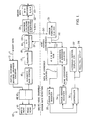
- FIG. 1 is a schematic showing of the write/read channel means of an exemplary disk drive having an partial response IV (PRIV) maximum likelihood coding. This figure also shows an error rate measuring/detection circuit means in accordance with the invention.
- PRIV partial response IV
- Class IV partial response coding is a three signal level form of partial response coding. Advance amplitude sampling coding and detection techniques, of which PRIV is an example, intentionally provide intersymbol interference. As a result, peak amplitude signal detection cannot be used to detect the binary content of the analog read back signal that is generated when such coded data is read back from the disk.
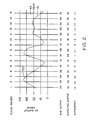
- FIG. 2 shows an exemplary analog read back signal 20, as it is generated by the disk drive read channel means of FIG. 1.
- the analog read signal that is derived from reading a magnetic track that has been recorded (i.e. written) by the use of the PRIV technique provides three critical signal amplitudes, labeled "Zero", "+A” and "-A” in FIG. 2.
- the values "+A” and "-A” comprises detection thresholds that enable the PRIV circuit means to detect the reading of binary 1's.
- FIG. 2 also contains the offset decimal values "32", “48” and “16", wherein the value "32” is associated with the above mentioned value "Zero".
- the decimal values "32", “48” and “16” represent the values of an offset binary numbering system whose values are provided by the output of analog to digital convertor (A/D) 19 shown in FIG. 1, as will be explained.
- PRIV analog read signal 20 of FIG. 2 contains positive and negative peak signal amplitudes that are caused by reading recorded magnetic transitions from the disk.
- the binary content of the recorded data is not contained in the time position of these peaks, as it is in the peak detection recording technology discussed above.
- PRIV coding the presence of a "Zero" signal amplitude at a clock interval represents (i.e. is decoded as) a binary "0", and the presence of either a "+A" of a "-A" threshold amplitude at a clock interval represents a binary "1".
- the top row of FIG. 2 contains a sequence of clock pulse times, labeled clock pulses 1 through 15.
- the amplitude of analog read signal 20 is decimal 50, see the row labeled "A/D output". Since the amplitude of signal 20 is above "+A" at clock time 2, the read signal sample amplitude of 50 is decoded as a binary "1" data bit by the disk drive's read channel.
- the expected value of decimal 48 see the row labeled "Expected Output" is compared to the actual value of signal 20, i.e. to the value 50, to thereby derive a difference value of +2 (i.e. the signal value was two units higher than was expected at clock pulse 2 for the reading of a binary "1").
- a difference value is provided for each clock pulse during the reading of the recorded data from the disk(s) of the disk drive being tested, see the row labeled "Difference".
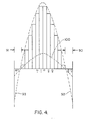
- the magnitude segregated collection of these difference values then form a testing means, such the histogram of FIG. 4, enabling the failure rate of the disk drive to be determined.
- this test can be performed without a failure to properly read binary recorded data actually occurring. That is, the expected A/D output values may all fall within values allowing proper decoding of binary "1" and "0", and yet in accordance with the invention, the history represented by the difference row of FIG. 2, and the histogram of FIG. 4, enables a failure rate of the disk drive to be determined with great accuracy.
- the output data of the present invention may, for example, comprise go/no-go test wherein rejected disk drives from a manufacturing process may be quickly determined.
- FIG. 1 is a schematic showing of the write channel and the read channel of an exemplary disk drive having a signal amplitude coding means in the write channel, and having a signal amplitude decoding means in the read channel, wherein the read channel's analog read signal is digitized, and the digitized values are connected to an error rate detection circuit means in accordance with the invention.
- the write portion 10 of a magnetic transducer 13 is first used to write a number of disk tracks with random input binary data, as is provided to the write channel by way of input conductor 11.
- the form that data 11 takes is not critical to the invention. However, in an embodiment of the invention it has been found advantageous to write random binary data.
- Data 11 is encoded to provide for amplitude sampling data detection during the subsequent reading back of the disk tracks.
- partial response maximum likelihood encoding network 12 is used to encode binary data 11 before the data is written to the disk tracks.
- write and read channels of FIG. 1 While the construction and arrangement of the write and read channels of FIG. 1 are not to be taken as a limitation on the invention, these two channels both include an arm electronics network (RE) network 15. As is well known by those skilled in the art, network 15 provides a variety of electronic functions, including for example amplification of the write/read signal.
- RE arm electronics network
- the read channel of FIG. 1 includes AE network 15, an automatic gain control network 16 and an equalization network 17.
- AE network 15-17 an analog read signal is present on conductor 18.
- This analog signal is connected to the input of A/D convertor 19.
- analog signal 20 of FIG. 2 is present on conductor
- analog values or amplitudes of signal 20 are sampled at clock times or intervals of a clock that is provided to A/D convertor 19 by way of conductor 21′ shown in FIG. 1.
- the frequency of this clock may be synchronized to read back signal 20 as is described in above mentioned application SN. 07/258,937, if desired.
- the disk drive read channel shown in FIG. 1 includes a maximum likelihood detector network 21 (also known in the art as an ML detector or a Verterbi detector).
- detector 21 The basic function of detector 21 is to decode the three significant A/D output values "Zero", "+A” and "-A” of FIG. 2 into binary "1” and "0" at each pulse of clock 21.
- a decode network 22 is also provided.
- the binary output 23 of network 22 comprises the original binary input 11 that was presented to the write channel during the writing of data to the disk drive.
- Dotted line conductor 30 connects the digitized sample signal output 24 of A/D convertor 19 (i.e. the row labeled "A/D output" in FIG. 2) to an error rate detection circuit means in accordance with the invention.
- Conductor 30 is dotted to indicate that the circuit means of the invention may be connected to conductor 24 only during the testing of the disk drive, or, alternatively, the circuit means of the invention may be formed as an integral portion of each disk drive, as the disk drive is manufactured.
- the output of A/D convertor 19 comprises a 6-bit binary word whose minimum value is "000000" (i.e. decimal 0) and whose maximum value is "111111” (i.e. decimal 63), as is shown in the following TABLES A-D.
- These decimal values, and more specifically the decimal values of 0, 16, 32, 48 and 64, comprise the vertical axis of FIG. 2.
- the pulses of clock 21 comprises the horizontal axis of FIG. 2.
- decimal values 16, 32 and 48 are significant values in that these values are the three expected values against which the digitized sample magnitudes of signal 20 are compared at the time of each clock pulse.
- analog read signal 20 is shown with the mid range A/D convertor output value of 32 as a base line for signal 20, i.e. the zero value of signal 20 is located on the horizontal value line 32 of FIG. 2.
- the various digitized signal values that comprise the output of A/D convertor 19 provide an offset binary numbering system by which the amplitude of analog read back signal 20 is determined.
- the 6-bit output of A/D convertor 19 is applied to the input of error function network 31.
- Network 31 operates to determine the difference between (1) the expected baseline value of 32 for analog signal 20, (2) the expected negative value of 16 for signal 20, or (3) the expected positive value of 32 for signal 20, at each of the respective pulses of clock 21.
- error function network 31 operates to map from the 64 different 6-bit input values that can be provided by output 24 of A/D convertor 19, to 16 different addressable storage locations within the 16x16 bit RAM shown in FIG. 1. Stated differently, error function network 31 operates to convert a 6-bit input on conductor 30 to a 4-bit output on conductor 32.
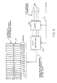
- FIG. 3 shows an embodiment of RAM 33 which includes 16 registers or counters, as will be described.
- error function network 31 has the effect of bracketing 16 sample error slots about each of the expected sample values of decimal 48, 32 and 16, which values are shown on the vertical axis of FIG. 2. Each of these slots corresponding to one of the sixteen different storage locations of RAM 33. This effectively puts error zones, represented by the storage locations, on each side of these expected values, with the addressing of storage location "0" representing a no error condition in a sample's magnitude.
- mapping function measures the difference between magnitude of a received sample value and the expected magnitude value for the sample, and causes the measured difference magnitude to be logged as one event into the corresponding storage location, i.e. a measured difference value of +3 is logged into the +3 storage location, as will be described.
- FIG. 4 is a representative histogram of the type that is provided by the various count magnitudes that are stored in the 16 addressable locations of RAM 33 after a disk drive has been tested in accordance with the invention.
- the horizontal axis of this figure presents the sixteen storage locations, starting with a storage location "-8" on at the left end of the horizontal axis, and progressing through storage location "0", to storage location "+7" at the right end of the horizontal axis.
- the vertical axis presents the relative count magnitudes that are stored in each storage location at the end of a test.
- storage location "-8" is addressed whenever the 4-bit output of error function network 31 comprises “0000”
- storage location "0” is addressed whenever the 4-bit output of error function network 31 comprises “1000”
- storage location "+7 ⁇ is addressed whenever the 4-bit output of error function network 31 comprises "1111”.
- the histogram of FIG. 4 may be generated by reading out the contents of the sixteen storage locations of RAM 33 after the testing of the disk drive. Controller 36, error address register 34 and error data register 35 are provided for this purpose. Controller 36 can then be used to drive display such as a cathode ray tube or a printer 37. In addition, controller 36 may provide a go/no-go output by way of pass/fail indicator or output means 38.
- the input to latch 49 comprises the 4-bit binary output word 32 from error function network 31, shown in FIG. 1.
- This input 32 includes the "difference" value row shown in FIG. 2.
- the 4-bit word values that are possible at input 32 cover the range of the sixteen binary values from “1111” to "0000”, and also covers a correspondingly defined 16-slot decimal range that extends from a decimal value of "+7” to a decimal value of "-8", as is defined by, and as will be described relative to, TABLES A-D.
- this binary word range is shown in FIG. 3 by way of a 4-bit address that is associated with each of the sixteen registers 51, wherein the sixteen individual registers are identified as "+7", "+6"--------"-7” and "-8". This convention is also used in the following TABLES A-D.
- a 4-bit binary number within the above range of numbers is presented as an input TO latch 49 at the time of the occurrence of each pulse of clock 21. This number is retained in latch 49 until the time of occurrence of the next clock pulse.
- Latch 49 presents this 4-bit number to multiplexer 50. Multiplexer 50 then operates to address one of the sixteen registers 51, and clock pulse 21 increments the content of that register by one count.
- register "+1" contains a count of "M”
- the next 4-bit difference word that is applied to the input of latch 49 is "1001" (for example, the difference row value of +1 that is measured at clock pulse 3 in FIG. 2). This event will cause the content of register "+1” to increment to the value "M+1".
- the measured difference values are magnitude segregated, and like magnitude difference values are counted.
- a microprocessor such as controller 36 of FIG. 1, can be used to address the individual registers 51 in order to generate an output such as at 37 and/or 38 of FIG. 1.
- error function network 31 maps from 64 different 6-bit input values, as is provided by the output of A/D convertor 19, to 16 different addressable locations within RAM 33 of FIG. 1, or to sixteen different addressable registers of FIG. 3. In this manner, counts are accumulated in each storage location or register, in accordance with the frequency with which each addressable location or register has been addressed during the testing of a disk drive.
- Error function network 31 has the effect of bracketing a 16 sample count or slot region about each of the expected sample values of decimal 48, 32 and 16 shown on the vertical axis of FIG. 2, each of these slots corresponding to one of the sixteen different storage locations or registers. This effectively puts error bars or zones, represented by the storage locations or registers, on each side of these expected values, with the addressing of storage location or register "0" representing a no error condition in a sample's magnitude.
- the above mentioned mapping function measures the difference between magnitude of a received sample value and the expected magnitude value for the sample, and causes the measured difference magnitude to be logged as one event into the corresponding storage location or register, i.e. a measured difference value of +3 is logged into the +3 register of FIG. 3.
- the column of the tables labeled "Register Incremented” refers to the register of FIG. 3 (sixteen registers, labeled “-8” through “+7” are provided in FIG. 3), whose number content is incremented by one count each time that error function network 31 generates the 4-bit address of the particular register. For example, each time the output of A/D convertor 19 provides one of the three expected outputs upon the occurrence of a pulse of clock 21 (i.e. one of the decimal values 48, 32 or 16 of FIG. 2), error function network 31 generates the 4-bit address "1000", and register "0" is addressed and incremented by one count. After the disk drive has been tested, it is usual that the count contained in registers "0" and "-1" are the highest of all registers, and are approximately equal in value, as is shown in the example histogram of FIG. 4.
- the column of the tables labeled "Register Incremented” also refers to the storage location of RAM 33 of FIG. 1 (sixteen storage locations are provided), whose number content is incremented by one count each time that error function network 31 generates the 4-bit address of the particular RAM storage location.
- 111000 (56) 1111 (15) +7 110111 (55) 1111 (15) +7 110110 1110 +6 110101 1101 +5 110100 1100 +4 110011 1011 +3 110010 (50) 1010 +2 110000 (49) 1010 +1 110000 (48) 1000 0 TABLE B A/D Output Error Function Output Address Increment Register 101111 (47) 0111 (7) -1 101110 0110 -2 101101 0101 -3 101100 0100 -4 101011 0011 -5 101010 0010 -6 101001 0001 -7 101000 (40) 0000 (0) -8 100111 (39) 1111 (15) +7 100110 1110 +6 100101 1101 +5 100100 1100 +4 100011 1011 +3 100010 (34) 1010 +2 100001 1010 +1 100000 (32) 1000 0 TABLE C A/D Output Error Function Output Address Increment Register 011111 (31) 0111 (7) -1 011110 (30) 0110 -2 011101 0101 -3 011
- FIG. 4 is a representative histogram of the type that is provided by the various count magnitudes that are stored in the sixteen storage locations of RAM 33 of FIG. 1, or in the sixteen registers of FIG. 3, after a disk drive has been tested in accordance with the invention.
- the horizontal axis of this figure presents the sixteen registers of FIG. 3, starting with register -8 on at the left end of the horizontal axis, and progressing through register 0, to register +7 at the right end of the horizontal axis.
- the vertical axis presents the relative count magnitudes that are stored in each register at the end of a test.
- the histogram of FIG. 4 may be generated by reading out the contents of the sixteen storage location of PAM 33, the sixteen registers shown in FIG. 3, after the testing of the disk drive, and then using this derived data to drive a display means such as a cathode ray tube or a printer 37 of FIG. 1.
- the histogram is shown as being quite symmetrical about the count values that are stored in registers 0 and -1. While this is a typical case, it need not be so. Also note that in this exemplary case, no counts were stored in the four end registers -8, -7, +6 and +7. This situation is an indication that the tested disk drive will be able to sustain a fairly high data rate before read back errors begin to occur.
- a manufacturing specification for disk drives of a given type may specify the minimum histogram dimension 90 and/or 91 that must exist in order for a disk drive to pass a manufacturing qualification test.
- Another approach to the use of a histogram in accordance with the invention is to extend the generally bell shaped curve, as at 92 and 93, in order to estimate at what data rate read errors will likely begin to occur. For example, a histogram such as is shown by dotted line 100 would likely indicate a failing disk drive, due to the flat slope exhibited by the two ends of the histogram curve.
- testing means in accordance with the invention is incorporated within each disk drive that is manufactured. In this way, operation of the invention can be performed periodically during the life of the disk drive, perhaps as a portion of periodic maintenance procedures.
Landscapes
- Engineering & Computer Science (AREA)
- Signal Processing (AREA)
- Signal Processing For Digital Recording And Reproducing (AREA)
Applications Claiming Priority (2)
| Application Number | Priority Date | Filing Date | Title |
|---|---|---|---|
| US07/429,750 US5121263A (en) | 1989-10-31 | 1989-10-31 | Method and apparatus for determining the error rate of magnetic recording disk drives having a amplitude sampling data detection |
| US429750 | 1989-10-31 |
Publications (3)
| Publication Number | Publication Date |
|---|---|
| EP0426353A2 true EP0426353A2 (fr) | 1991-05-08 |
| EP0426353A3 EP0426353A3 (en) | 1991-11-13 |
| EP0426353B1 EP0426353B1 (fr) | 1995-07-05 |
Family
ID=23704589
Family Applications (1)
| Application Number | Title | Priority Date | Filing Date |
|---|---|---|---|
| EP90311573A Expired - Lifetime EP0426353B1 (fr) | 1989-10-31 | 1990-10-22 | Détermination du taux d'erreur pour des dispositifs de stockage de données |
Country Status (4)
| Country | Link |
|---|---|
| US (1) | US5121263A (fr) |
| EP (1) | EP0426353B1 (fr) |
| JP (1) | JPH0785341B2 (fr) |
| DE (1) | DE69020685T2 (fr) |
Cited By (12)
| Publication number | Priority date | Publication date | Assignee | Title |
|---|---|---|---|---|
| EP0559277A1 (fr) * | 1992-03-04 | 1993-09-08 | Koninklijke Philips Electronics N.V. | Dispositif d'enregistrement d'information |
| EP0581717A3 (en) * | 1992-07-30 | 1995-12-20 | Ibm | Error measurement circuit |
| GB2336464A (en) * | 1998-04-15 | 1999-10-20 | Samsung Electronics Co Ltd | Detecting defects in hard disk drives |
| EP0844758A3 (fr) * | 1996-11-22 | 2001-11-28 | Lsi Logic Corporation | Récepteur digital non égalisé utilisant un décodage par blocs avec correction d'effacements et d'erreurs |
| EP1146514A4 (fr) * | 1999-01-18 | 2002-05-15 | Fujitsu Ltd | Technique et dispositif d'extraction de donnees et dispositif a disque optique |
| WO2003003367A1 (fr) * | 2001-06-29 | 2003-01-09 | Infineon Technologies North America Corp. | Emulateur de brouillage hors voie |
| US6556006B1 (en) | 2001-11-21 | 2003-04-29 | Samsung Electronics Co., Ltd. | Method for magneto-resistive head electrostatic popping detection |
| US6744597B2 (en) | 1999-10-29 | 2004-06-01 | Samsung Electronics Co., Ltd. | Dynamic absorber for an actuator arm in a disk drive |
| US6762908B2 (en) | 2001-06-18 | 2004-07-13 | Samsung Electronics Co., Ltd. | Air razor and disk limiter for a hard disk drive |
| US6791778B2 (en) | 2000-09-14 | 2004-09-14 | Samsung Electronics Co., Inc. | Method and apparatus to detect and manage servo sectors with defect on servo pattern area in hard disk drives |
| US6791775B2 (en) | 2001-10-15 | 2004-09-14 | Samsung Electronics, Co., Inc. | Method and apparatus to distinguish effects of adjacent track encroachment from head thermal movement |
| US6947252B2 (en) | 2000-05-10 | 2005-09-20 | Samsung Electronics Co., Ltd. | Wave stringer for controlling acoustic noise and shock vibration in a storage device |
Families Citing this family (57)
| Publication number | Priority date | Publication date | Assignee | Title |
|---|---|---|---|---|
| US5450609A (en) * | 1990-11-13 | 1995-09-12 | Compaq Computer Corp. | Drive array performance monitor |
| US5220466A (en) * | 1991-05-21 | 1993-06-15 | International Business Machines Corporation | Method and apparatus for digital filter control in a partial-response maximum-likelihood disk drive system |
| US5357520A (en) * | 1992-01-31 | 1994-10-18 | International Business Machines Corporation | Method and apparatus for precompensation value determination in a PRML data channel |
| JP2948016B2 (ja) * | 1992-03-19 | 1999-09-13 | 株式会社日立製作所 | 情報記録再生方法 |
| US5341249A (en) * | 1992-08-27 | 1994-08-23 | Quantum Corporation | Disk drive using PRML class IV sampling data detection with digital adaptive equalization |
| US5268848A (en) * | 1992-09-30 | 1993-12-07 | International Business Machines Corporation | Equalizer adjustment for partial-response maximum-likelihood disk drive systems |
| US5295128A (en) * | 1992-10-28 | 1994-03-15 | International Business Machines Corporation | Clock controller employing a discrete time control loop method for clocking data in an asynchronous channel |
| US5353172A (en) * | 1992-11-04 | 1994-10-04 | Alioth Henry L | Method of helical tape tracking adjustment using histogram of signal quality versus tape advance distance |
| US5424881A (en) * | 1993-02-01 | 1995-06-13 | Cirrus Logic, Inc. | Synchronous read channel |
| US5724205A (en) * | 1993-03-19 | 1998-03-03 | Goldstar Co., Ltd. | Automatic tracking control device which uses different weightings with a number of incorrectable, correctable, and non-errors |
| US5761212A (en) * | 1993-07-01 | 1998-06-02 | Cirrus Logic, Inc. | Channel quality |
| US5754353A (en) * | 1993-07-01 | 1998-05-19 | Cirrus Logic, Inc. | Channel quality circuit in a sampled amplitude read channel |
| US5444686A (en) * | 1993-09-28 | 1995-08-22 | Dunlavy; John H. | Method and apparatus for correcting distortion in compact disc recording and playback system |
| US5373400A (en) * | 1993-12-01 | 1994-12-13 | Analog Devices, Inc. | Dynamic threshold updating circuit for a maximum likelihood detector using both positive and negative comparators |
| US5355261A (en) * | 1993-12-20 | 1994-10-11 | Guzik Technical Enterprises, Inc. | Method and apparatus for measuring error rate of magnetic recording devices having a partial response maximum likelihood data detection channel |
| US5515220A (en) * | 1993-12-30 | 1996-05-07 | Alioth; Henry L. | Multielement disk-shaped rotary magnetic media scanners for magnetic media player-recorders |
| US5490091A (en) * | 1994-03-01 | 1996-02-06 | Guzik Technical Enterprises, Inc. | Histograms of processed noise samples for measuring error rate of a PRML data detection channel |
| US6313961B1 (en) | 1994-04-29 | 2001-11-06 | Cirrus Logic, Inc. | Method and apparatus for calibrating a synchronous read channel integrated circuit |
| JP3351163B2 (ja) * | 1994-07-27 | 2002-11-25 | 株式会社日立製作所 | 情報記録再生装置及び信号処理回路 |
| JP3599383B2 (ja) | 1994-09-20 | 2004-12-08 | 株式会社日立グローバルストレージテクノロジーズ | 磁気記録再生装置及びデータエラーレート測定方法 |
| US5987634A (en) * | 1994-11-17 | 1999-11-16 | Cirrus Logic, Inc. | Channel quality circuit in a sampled amplitude read channel |
| JPH08249133A (ja) * | 1994-12-15 | 1996-09-27 | Internatl Business Mach Corp <Ibm> | ディスク・ドライブ・アレイの故障対策の方法及びシステム |
| US5557482A (en) * | 1994-12-19 | 1996-09-17 | International Business Machines Corporation | Multipath channel apparatus and method for data storage devices and communications systems wherein a data path is selected based on errors |
| US6032262A (en) * | 1995-04-18 | 2000-02-29 | Emc Corporation | Disk drive reliability determination system and method |
| US5633767A (en) * | 1995-06-06 | 1997-05-27 | International Business Machines Corporation | Adaptive and in-situ load/unload damage estimation and compensation |
| US5872672A (en) * | 1996-02-16 | 1999-02-16 | International Business Machines Corporation | System and method for monitoring and analyzing tape servo performance |
| US5914827A (en) * | 1996-02-28 | 1999-06-22 | Silicon Systems, Inc. | Method and apparatus for implementing a noise generator in an integrated circuit disk drive read channel |
| US5786951A (en) * | 1996-06-05 | 1998-07-28 | Cirrus Logic, Inc. | Sampled amplitude read channel employing a discrete time noise generator for calibration |
| US6000052A (en) * | 1996-07-22 | 1999-12-07 | Seagate Technology, Inc. | Signal conditioning system for controlling data retrieval channel characteristics in which errors in samples are segregated by association with intended sample values to control selected characteristics |
| US6016463A (en) * | 1996-08-26 | 2000-01-18 | Texas Instruments Incorporated | Channel quality monitor for read channel IC |
| US6134065A (en) * | 1996-09-06 | 2000-10-17 | U.S. Philips Corporation | Method and device utilizing erasure information as a reliability indicator in an information medium |
| US5838153A (en) * | 1996-12-13 | 1998-11-17 | Phase Metrics, Inc. | Magnetic media tester which includes a filter that filters the product of a read signal and an output of a phase lock loop circuit |
| US5895438A (en) * | 1996-12-23 | 1999-04-20 | Hitachi Computer Products (America ), Inc. | Inline disk tester |
| US6442730B1 (en) | 1997-01-27 | 2002-08-27 | Lecroy Corporation | Recording medium failure analysis apparatus and method |
| JP3887062B2 (ja) * | 1997-05-08 | 2007-02-28 | 株式会社東芝 | ディスク装置及び同装置に適用されるスループット・パフォーマンス測定方法 |
| US6877116B1 (en) | 1997-08-28 | 2005-04-05 | Seagate Technology Llc | Method and apparatus for determining bit error rate in a sampled data system without requiring read channel circuitry |
| KR100424131B1 (ko) * | 1997-08-28 | 2004-03-24 | 시게이트 테크놀로지 엘엘씨 | 샘플링된 데이터 시스템의 비트 에러율을 결정하는 방법 및 장치 |
| US6292912B1 (en) | 1998-02-27 | 2001-09-18 | Western Digital Technologies, Inc. | Disk drive having built-in self-test system for characterizing performance of the drive |
| US6181499B1 (en) * | 1998-04-07 | 2001-01-30 | International Business Machines Corporation | Method and apparatus for testing the digital read channel circuit of a data storage device |
| US6704161B1 (en) | 1998-11-06 | 2004-03-09 | Samsung Electronics Co. Ltd. | Shock protection skin bumper for a hard disk drive |
| US6417986B1 (en) | 1998-11-16 | 2002-07-09 | Samsung Electronics Co., Ltd. | Impact guard for limiting hard disk movement |
| US6549372B1 (en) | 1998-12-15 | 2003-04-15 | Samsung Electronics Co., Ltd | Device for limiting head movement within a hard disk drive |
| US6417994B1 (en) | 1999-04-22 | 2002-07-09 | Samsung Electronics, Co., Ltd. | Swage plate with protruded walls to increase retention torque in hard disk applications |
| JP4077993B2 (ja) | 1999-07-30 | 2008-04-23 | 株式会社日立グローバルストレージテクノロジーズ | 性能評価方法及び性能評価装置並びにこれらを用いた記録再生装置 |
| US6501614B1 (en) | 1999-08-19 | 2002-12-31 | Samsung Electronics Co., Ltd. | Acoustic insulator for controlling noise generated in a mass storage device |
| US6604211B1 (en) | 1999-08-31 | 2003-08-05 | Seagate Technology Llc | Tool for initiating and analyzing error recovery procedures in data storage devices |
| US6384599B1 (en) | 2000-02-01 | 2002-05-07 | International Business Machines Corporation | System, method, and program for analyzing offset track errors in a storage system |
| US6446517B1 (en) | 2000-11-20 | 2002-09-10 | Samsung Electronics Company | Controlled particle deposition in drives and on media for thermal asperity studies |
| US6590738B2 (en) | 2001-03-01 | 2003-07-08 | Samsung Electronics Co., Ltd. | Particle removal device in a hard disk drive |
| US6777929B2 (en) | 2002-08-27 | 2004-08-17 | International Business Machines Corporation | Cross talk bit error rate testing of a magnetic head |
| US7506236B2 (en) * | 2004-05-28 | 2009-03-17 | International Business Machines Corporation | Techniques for operating semiconductor devices |
| US7193801B2 (en) * | 2004-11-18 | 2007-03-20 | Agere Systems, Inc. | Method and apparatus for testing a servo circuit of a read/write head system |
| US7562282B1 (en) | 2005-05-23 | 2009-07-14 | Western Digital Technologies, Inc. | Disk drive employing error threshold counters to generate an ECC error distribution |
| US7529049B2 (en) | 2006-09-01 | 2009-05-05 | Hitachi Global Storage Technologies Netherlands B.V. | Method and system for testing of magnetic disks using F-BER |
| JP4748100B2 (ja) * | 2007-05-08 | 2011-08-17 | Tdk株式会社 | 光記録再生の信号評価方法、光記録再生方法 |
| TWI391918B (zh) * | 2009-06-15 | 2013-04-01 | Novatek Microelectronics Corp | 資料復原裝置與方法 |
| US9099159B1 (en) | 2013-08-06 | 2015-08-04 | Western Digital Technologies, Inc. | Disk drive generating quality metric map for a data track while in different configurations |
Family Cites Families (8)
| Publication number | Priority date | Publication date | Assignee | Title |
|---|---|---|---|---|
| US4394695A (en) * | 1981-02-02 | 1983-07-19 | Sharp Corporation | Method and apparatus for evaluating recording systems |
| JPS57208613A (en) * | 1981-06-15 | 1982-12-21 | Nippon Denso Co Ltd | Magnetic recorder and reproducer |
| US4504872A (en) * | 1983-02-08 | 1985-03-12 | Ampex Corporation | Digital maximum likelihood detector for class IV partial response |
| JPS60115073A (ja) * | 1983-11-28 | 1985-06-21 | Matsushita Electric Ind Co Ltd | 光情報記録再生装置 |
| US4578721A (en) * | 1984-09-10 | 1986-03-25 | Seagate Technology | Stress test for magnetic disc recording apparatus |
| US4574234A (en) * | 1984-09-26 | 1986-03-04 | Applied Magnetics Corporation | System for measuring selected parameters of electrical signals and method |
| IE60167B1 (en) * | 1987-06-10 | 1994-06-15 | Benares Limited | Method and apparatus for testing characteristics of a flop disc and floppy disc drive |
| US4970609A (en) * | 1988-10-17 | 1990-11-13 | International Business Machines Corporation | Clocking method and apparatus for use with partial response coded binary data |
-
1989
- 1989-10-31 US US07/429,750 patent/US5121263A/en not_active Expired - Lifetime
-
1990
- 1990-10-15 JP JP2273512A patent/JPH0785341B2/ja not_active Expired - Fee Related
- 1990-10-22 DE DE69020685T patent/DE69020685T2/de not_active Expired - Fee Related
- 1990-10-22 EP EP90311573A patent/EP0426353B1/fr not_active Expired - Lifetime
Cited By (18)
| Publication number | Priority date | Publication date | Assignee | Title |
|---|---|---|---|---|
| EP0559277A1 (fr) * | 1992-03-04 | 1993-09-08 | Koninklijke Philips Electronics N.V. | Dispositif d'enregistrement d'information |
| EP0581717A3 (en) * | 1992-07-30 | 1995-12-20 | Ibm | Error measurement circuit |
| EP0844758A3 (fr) * | 1996-11-22 | 2001-11-28 | Lsi Logic Corporation | Récepteur digital non égalisé utilisant un décodage par blocs avec correction d'effacements et d'erreurs |
| GB2336464A (en) * | 1998-04-15 | 1999-10-20 | Samsung Electronics Co Ltd | Detecting defects in hard disk drives |
| GB2336464B (en) * | 1998-04-15 | 2000-08-02 | Samsung Electronics Co Ltd | Detecting defects in hard disk drives |
| US6151180A (en) * | 1998-04-15 | 2000-11-21 | Samsung Electronics Co., Ltd. | Method and apparatus for detecting defects on a disk in a hard disk drive |
| EP1146514A4 (fr) * | 1999-01-18 | 2002-05-15 | Fujitsu Ltd | Technique et dispositif d'extraction de donnees et dispositif a disque optique |
| US6618338B1 (en) | 1999-01-18 | 2003-09-09 | Fujitsu Limited | Data reproduction control method and apparatus, and optical disk unit |
| US6714504B2 (en) | 1999-01-18 | 2004-03-30 | Fujitsu Limited | Data reproduction control method and apparatus, and optical disk unit |
| US6775219B2 (en) | 1999-01-18 | 2004-08-10 | Fujitsu Limited | Data reproduction control method and apparatus, and optical disk unit |
| US6744597B2 (en) | 1999-10-29 | 2004-06-01 | Samsung Electronics Co., Ltd. | Dynamic absorber for an actuator arm in a disk drive |
| US6947252B2 (en) | 2000-05-10 | 2005-09-20 | Samsung Electronics Co., Ltd. | Wave stringer for controlling acoustic noise and shock vibration in a storage device |
| US6791778B2 (en) | 2000-09-14 | 2004-09-14 | Samsung Electronics Co., Inc. | Method and apparatus to detect and manage servo sectors with defect on servo pattern area in hard disk drives |
| US6762908B2 (en) | 2001-06-18 | 2004-07-13 | Samsung Electronics Co., Ltd. | Air razor and disk limiter for a hard disk drive |
| US6771442B2 (en) | 2001-06-29 | 2004-08-03 | Infineon Technologies Ag | Off-track interference emulator |
| WO2003003367A1 (fr) * | 2001-06-29 | 2003-01-09 | Infineon Technologies North America Corp. | Emulateur de brouillage hors voie |
| US6791775B2 (en) | 2001-10-15 | 2004-09-14 | Samsung Electronics, Co., Inc. | Method and apparatus to distinguish effects of adjacent track encroachment from head thermal movement |
| US6556006B1 (en) | 2001-11-21 | 2003-04-29 | Samsung Electronics Co., Ltd. | Method for magneto-resistive head electrostatic popping detection |
Also Published As
| Publication number | Publication date |
|---|---|
| EP0426353B1 (fr) | 1995-07-05 |
| JPH03144969A (ja) | 1991-06-20 |
| DE69020685T2 (de) | 1996-03-07 |
| JPH0785341B2 (ja) | 1995-09-13 |
| EP0426353A3 (en) | 1991-11-13 |
| DE69020685D1 (de) | 1995-08-10 |
| US5121263A (en) | 1992-06-09 |
Similar Documents
| Publication | Publication Date | Title |
|---|---|---|
| EP0426353B1 (fr) | Détermination du taux d'erreur pour des dispositifs de stockage de données | |
| US6292912B1 (en) | Disk drive having built-in self-test system for characterizing performance of the drive | |
| US6731442B2 (en) | Method and apparatus for detecting media defects | |
| US5761212A (en) | Channel quality | |
| US4881136A (en) | Method and apparatus for detecting minute defects on magnetic disk by monitoring both amplitude decrease and phase shift of a reproduced signal | |
| JP3605091B2 (ja) | 変換ヘッドのディスク表面上での位置を決定するための方法及びディスクドライブ | |
| US4958337A (en) | Disk recording checking method for determining if a disk is defective by the number of errors present | |
| US4578721A (en) | Stress test for magnetic disc recording apparatus | |
| US4754222A (en) | Method for detecting and evaluating dropouts in recording media having digital signals recorded thereon | |
| US7032127B1 (en) | Method and apparatus for identifying defective areas on a disk surface of a disk drive based on defect density | |
| US3639900A (en) | Enhanced error detection and correction for data systems | |
| US6175460B1 (en) | Magnetic recording and reproduction apparatus | |
| US4929894A (en) | Method and apparatus for increasing throughput on disk drive quality control testing | |
| US3755731A (en) | System for detecting dropout and noise characteristics of magnetic tape with switch means to select which characteristics to be detected | |
| US6366081B1 (en) | Method and apparatus for high throughput media defect testing using true reference value | |
| CA1322406C (fr) | Appareil de lecture de signaux numeriques | |
| EP0392382A2 (fr) | Appareil pour contrôler la correction d'erreurs | |
| TW367491B (en) | Magnetic disk certifier | |
| KR910003378B1 (ko) | 디지탈 신호 복조 및 재생장치 | |
| JPS6138476A (ja) | 記録媒体欠陥検出装置 | |
| CA1231440A (fr) | Canal de lecture pour enregistreur optique | |
| JPS59144013A (ja) | マルチトラツク記録装置のエラ−測定装置 | |
| JP2954104B2 (ja) | バルクハウゼンノイズ検出方法 | |
| JPS60115073A (ja) | 光情報記録再生装置 | |
| Baugh et al. | Extremely low error rate digital recording with a helical scan recorder |
Legal Events
| Date | Code | Title | Description |
|---|---|---|---|
| PUAI | Public reference made under article 153(3) epc to a published international application that has entered the european phase |
Free format text: ORIGINAL CODE: 0009012 |
|
| 17P | Request for examination filed |
Effective date: 19901213 |
|
| AK | Designated contracting states |
Kind code of ref document: A2 Designated state(s): DE FR GB |
|
| PUAL | Search report despatched |
Free format text: ORIGINAL CODE: 0009013 |
|
| AK | Designated contracting states |
Kind code of ref document: A3 Designated state(s): DE FR GB |
|
| 17Q | First examination report despatched |
Effective date: 19940520 |
|
| GRAA | (expected) grant |
Free format text: ORIGINAL CODE: 0009210 |
|
| AK | Designated contracting states |
Kind code of ref document: B1 Designated state(s): DE FR GB |
|
| REF | Corresponds to: |
Ref document number: 69020685 Country of ref document: DE Date of ref document: 19950810 |
|
| ET | Fr: translation filed | ||
| PGFP | Annual fee paid to national office [announced via postgrant information from national office to epo] |
Ref country code: GB Payment date: 19950926 Year of fee payment: 6 |
|
| PGFP | Annual fee paid to national office [announced via postgrant information from national office to epo] |
Ref country code: FR Payment date: 19951009 Year of fee payment: 6 |
|
| PGFP | Annual fee paid to national office [announced via postgrant information from national office to epo] |
Ref country code: DE Payment date: 19951030 Year of fee payment: 6 |
|
| PLBE | No opposition filed within time limit |
Free format text: ORIGINAL CODE: 0009261 |
|
| STAA | Information on the status of an ep patent application or granted ep patent |
Free format text: STATUS: NO OPPOSITION FILED WITHIN TIME LIMIT |
|
| 26N | No opposition filed | ||
| PG25 | Lapsed in a contracting state [announced via postgrant information from national office to epo] |
Ref country code: GB Effective date: 19961022 |
|
| GBPC | Gb: european patent ceased through non-payment of renewal fee |
Effective date: 19961022 |
|
| PG25 | Lapsed in a contracting state [announced via postgrant information from national office to epo] |
Ref country code: FR Effective date: 19970630 |
|
| PG25 | Lapsed in a contracting state [announced via postgrant information from national office to epo] |
Ref country code: DE Effective date: 19970701 |
|
| REG | Reference to a national code |
Ref country code: FR Ref legal event code: ST |