EP0427285B1 - Verfahren zur Herstellung mit hoher Strahlungsbeständigkeit - Google Patents
Verfahren zur Herstellung mit hoher Strahlungsbeständigkeit Download PDFInfo
- Publication number
- EP0427285B1 EP0427285B1 EP90121469A EP90121469A EP0427285B1 EP 0427285 B1 EP0427285 B1 EP 0427285B1 EP 90121469 A EP90121469 A EP 90121469A EP 90121469 A EP90121469 A EP 90121469A EP 0427285 B1 EP0427285 B1 EP 0427285B1
- Authority
- EP
- European Patent Office
- Prior art keywords
- oxide film
- film
- boron
- manufacturing
- semiconductor substrate
- Prior art date
- Legal status (The legal status is an assumption and is not a legal conclusion. Google has not performed a legal analysis and makes no representation as to the accuracy of the status listed.)
- Expired - Lifetime
Links
Images


Classifications
-
- H—ELECTRICITY
- H10—SEMICONDUCTOR DEVICES; ELECTRIC SOLID-STATE DEVICES NOT OTHERWISE PROVIDED FOR
- H10D—INORGANIC ELECTRIC SEMICONDUCTOR DEVICES
- H10D64/00—Electrodes of devices having potential barriers
- H10D64/01—Manufacture or treatment
- H10D64/013—Manufacture or treatment of electrodes having a conductor capacitively coupled to a semiconductor by an insulator
- H10D64/01302—Manufacture or treatment of electrodes having a conductor capacitively coupled to a semiconductor by an insulator the insulator being formed after the semiconductor body, the semiconductor being silicon
- H10D64/01332—Making the insulator
- H10D64/01336—Making the insulator on single crystalline silicon, e.g. chemical oxidation using a liquid
- H10D64/01338—Making the insulator on single crystalline silicon, e.g. chemical oxidation using a liquid with a treatment, e.g. annealing, after the formation of the conductor
-
- H—ELECTRICITY
- H10—SEMICONDUCTOR DEVICES; ELECTRIC SOLID-STATE DEVICES NOT OTHERWISE PROVIDED FOR
- H10D—INORGANIC ELECTRIC SEMICONDUCTOR DEVICES
- H10D64/00—Electrodes of devices having potential barriers
- H10D64/01—Manufacture or treatment
- H10D64/013—Manufacture or treatment of electrodes having a conductor capacitively coupled to a semiconductor by an insulator
- H10D64/01302—Manufacture or treatment of electrodes having a conductor capacitively coupled to a semiconductor by an insulator the insulator being formed after the semiconductor body, the semiconductor being silicon
- H10D64/01332—Making the insulator
- H10D64/01336—Making the insulator on single crystalline silicon, e.g. chemical oxidation using a liquid
-
- H—ELECTRICITY
- H10—SEMICONDUCTOR DEVICES; ELECTRIC SOLID-STATE DEVICES NOT OTHERWISE PROVIDED FOR
- H10D—INORGANIC ELECTRIC SEMICONDUCTOR DEVICES
- H10D64/00—Electrodes of devices having potential barriers
- H10D64/60—Electrodes characterised by their materials
- H10D64/66—Electrodes having a conductor capacitively coupled to a semiconductor by an insulator, e.g. MIS electrodes
- H10D64/68—Electrodes having a conductor capacitively coupled to a semiconductor by an insulator, e.g. MIS electrodes characterised by the insulator, e.g. by the gate insulator
-
- H—ELECTRICITY
- H10—SEMICONDUCTOR DEVICES; ELECTRIC SOLID-STATE DEVICES NOT OTHERWISE PROVIDED FOR
- H10P—GENERIC PROCESSES OR APPARATUS FOR THE MANUFACTURE OR TREATMENT OF DEVICES COVERED BY CLASS H10
- H10P32/00—Diffusion of dopants within, into or out of wafers, substrates or parts of devices
- H10P32/20—Diffusion for doping of insulating layers
-
- H—ELECTRICITY
- H10—SEMICONDUCTOR DEVICES; ELECTRIC SOLID-STATE DEVICES NOT OTHERWISE PROVIDED FOR
- H10W—GENERIC PACKAGES, INTERCONNECTIONS, CONNECTORS OR OTHER CONSTRUCTIONAL DETAILS OF DEVICES COVERED BY CLASS H10
- H10W10/00—Isolation regions in semiconductor bodies between components of integrated devices
- H10W10/01—Manufacture or treatment
- H10W10/011—Manufacture or treatment of isolation regions comprising dielectric materials
- H10W10/012—Manufacture or treatment of isolation regions comprising dielectric materials using local oxidation of silicon [LOCOS]
- H10W10/0125—Manufacture or treatment of isolation regions comprising dielectric materials using local oxidation of silicon [LOCOS] comprising introducing electrical impurities in local oxidation regions, e.g. to alter LOCOS oxide growth characteristics
-
- H—ELECTRICITY
- H10—SEMICONDUCTOR DEVICES; ELECTRIC SOLID-STATE DEVICES NOT OTHERWISE PROVIDED FOR
- H10W—GENERIC PACKAGES, INTERCONNECTIONS, CONNECTORS OR OTHER CONSTRUCTIONAL DETAILS OF DEVICES COVERED BY CLASS H10
- H10W10/00—Isolation regions in semiconductor bodies between components of integrated devices
- H10W10/10—Isolation regions comprising dielectric materials
- H10W10/13—Isolation regions comprising dielectric materials formed using local oxidation of silicon [LOCOS], e.g. sealed interface localised oxidation [SILO] or side-wall mask isolation [SWAMI]
-
- H—ELECTRICITY
- H10—SEMICONDUCTOR DEVICES; ELECTRIC SOLID-STATE DEVICES NOT OTHERWISE PROVIDED FOR
- H10D—INORGANIC ELECTRIC SEMICONDUCTOR DEVICES
- H10D64/00—Electrodes of devices having potential barriers
- H10D64/01—Manufacture or treatment
- H10D64/013—Manufacture or treatment of electrodes having a conductor capacitively coupled to a semiconductor by an insulator
- H10D64/01302—Manufacture or treatment of electrodes having a conductor capacitively coupled to a semiconductor by an insulator the insulator being formed after the semiconductor body, the semiconductor being silicon
- H10D64/01332—Making the insulator
- H10D64/01336—Making the insulator on single crystalline silicon, e.g. chemical oxidation using a liquid
- H10D64/01346—Making the insulator on single crystalline silicon, e.g. chemical oxidation using a liquid in a gaseous ambient using an oxygen or a water vapour, e.g. oxidation through a layer
Definitions
- the present invention relates to a method of manufacturing a radiation resistant semiconductor device used in, e.g., a space satellite, or a nuclear power plant.
- a guard-band structure (H. Hietano et al., "A Radiation-Hardened 10K-Gate CMOS Gate Array", IEEE Transactions on Nuclear Science, Vol. 36, No. 6, pages 2435 to 2438, December 1989) is employed to the field oxide film, the field oxide film is formed at a low temperature, or the field oxide film is made of two layers.
- a decrease in thickness and a treatment at a low temperature are effective to hardening of an oxide film.
- the present invention is made in consideration of the above drawbacks, and has as its object to provide a method of manufacturing a radiation resistant semiconductor device, capable of manufacturing semiconductor devices having good radiation resistance.
- a method of manufacturing a radiation resistant semiconductor device comprising the steps of forming an oxide film on a semiconductor substrate, depositing a metallic boron film on the oxide film, and diffusing boron from the metallic boron film to the oxide film by annealing.
- a method of manufacturing a radiation resistant semiconductor device comprising the steps of forming an element isolation oxide film and a gate insulating oxide film on a semiconductor substrate, depositing a metallic boron film on the element isolation oxide film and the gate insulating oxide film, and diffusing boron from the metallic boron film to the element isolation oxide film and the gate insulating oxide film by annealing.
- a method of manufacturing a radiation resistant semiconductor device comprising the steps of depositing a silicon nitride film on a semiconductor substrate, patterning the silicon nitride film to leave the silicon nitride film in a region where an element isolation oxide film is not formed, forming the element isolation oxide film by oxidization, depositing a metallic boron film on the entire surface of the silicon substrate; and diffusing metallic boron from the metallic boron film to the element isolation oxide film by annealing.
- a method of manufacturing a radiation resistant semiconductor device comprising the steps of forming a gate electrode on a semiconductor substrate, depositing an oxide film on the gate electrode, depositing a metallic boron film on the oxide film, diffusing boron from the metallic boron film to the oxide film by annealing, and leaving the oxide film on only the side walls of the gate electrode with an anisotropical etching method.
- a method of manufacturing a radiation resistant semiconductor device comprising the steps of forming an oxide film on a semiconductor substrate, depositing a film containing at least one element selected from a group consisting of boron, phosphorus, and arsenic on the oxide film, and diffusing at least one selected from the group consisting of boron, phosphorus, and arsenic from the film to the oxide film by annealing.
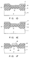
- Figs. 1A to 1F are sectional views showing the steps of a first manufacturing method when the present invention is employed to manufacture a MOS transistor.
- a field oxide film 12 and a gate oxide film 13 are formed on a p-type silicon semiconductor substrate 11 by a selective oxidation method, and a polysilicon film 14 is formed thereon by a CVD method (chemical vapor deposition method) or the like.
- a metallic boron film 15 is deposited on the polysilicon film 14 by a vacuum deposition method to have a thickness of about 0.1 ⁇ m.
- the resultant structure is annealed at a temperature of 900°C or more in a non-oxidizing atmosphere to diffuse the boron (B) from the metallic boron film 15 to both the field oxide film 12 and the gate oxide film 13 using the polysilicon film 14 as a buffer member, so as to form a boron doped region 16 on the surface of both the field oxide film 12 and the gate oxide film 13.
- the metallic boron atoms are doped by an implantation, the oxide films may be seriously damaged by the implanted ions. For this reason, an amount of trapped charges may be more significantly increased than those without implantations. Therefore, according to the present invention, the metallic boron atoms are diffused by annealing. Thereafter, the metallic boron film 15 is removed, and the polysilicon film 14 thereunder is removed to expose the surfaces of the field oxide film 12 and the gate oxide film 13.
- a polysilicon film 17 is deposited on the surface of the field oxide film 12 and the gate oxide film 13, and phosphorus is doped in the polysilicon film 17.
- the phosphorus may have a concentration at which the electric resistance of the gate electrode is satisfactorily low.
- the phosphorus doped in the polysilicon film 17 is further diffused by annealing.
- the boron atoms are diffused from the boron doped region 16 of the field oxide film 12 and the gate oxide film 13.
- the diffusion step is stopped.
- a time required for the diffusion step is determined in consideration of the thickness of the gate oxide film 13.
- the polysilicon film 17 is patterned using a predetermined mask by a selective etching method to form a gate electrode 18. Thereafter, an n-type impurity such as arsenic (As) is implanted in the surface of the substrate 11 and is activated to form a pair of n-type regions 19 and 20 serving as source and drain regions.
- n-type impurity such as arsenic (As)
- the boron atoms are doped in both the field oxide film 12 and the gate oxide film 13. Electrons generated by radiation exposure are caught once by traps formed by the boron atoms, and then the electrons are recombined with the holes at a high probability. As a result, the number of the holes available for trapping in the field oxide film 12 and the gate oxide film 13 is largely decreased compared with the conventional techniques.
- a guard-band structure need not be employed, a semiconductor device can be easily designed.
- the field oxide film can be formed at a relatively high temperature, a conventional manufacturing process can be easily applied to easily manufacturing a radiation resistant semiconductor device.
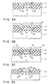
- Figs. 2A to 2C are sectional views showing the steps of a second manufacturing method of the present invention when the present invention is applied to the manufacturing of a MOS transistor with boron doped only in field oxide.
- a selective oxidation mask member such as a silicon nitride film 22 having a predetermined pattern is formed on a p-type silicon semiconductor substrate 21.
- a field oxide film 23 is formed on the substrate 21 by a thermal oxidation method using the silicon nitride film 22 as a mask.
- a metallic boron film 24 is deposited on an entire surface of the resultant structure by a vacuum deposition method or the like to have a thickness of about 0.1 ⁇ m.
- the resultant structure is annealed in a non-oxidizing atmosphere at a temperature of 900°C or more to diffuse the boron from the metallic boron film 24 to the field oxide film 23 so as to form a boron doped region 25.
- the time required for the diffusion step is determined in consideration of the thickness of the field oxide film 23. Since the silicon nitride film 22 is left on the surface of the substrate 21 where the field oxide film 23 is not formed, the boron atoms are not diffused in the substrate 21.
- the metallic boron film 24 and the silicon nitride film 22 are removed to expose the surfaces of the field oxide film 23 and the substrate 21. Therefore, a gate oxide film is formed, and a gate electrode and a pair of n + -type regions (neither are shown) serving as source and drain regions are formed.
- the boron atoms are doped in the field oxide film 23 by diffusion step before the gate oxide film is formed, the boron can be diffused in the field oxide film to a sufficiently deep depth without considering the thickness of the gate oxide film which is generally thinner than the field oxide film. Therefore, the holes trapped in the field oxide film 23 can be extremely reduced.
- the boron may be doped in the gate oxide film in another step.
- Figs. 3A to 3D are sectional views showing a third manufacturing method of the present invention when the present invention is applied to the manufacturing of a small-geometry LDD transistor.
- a field oxide film 32 and a gate oxide film 33 are formed on a p-type silicon semiconductor substrate 31 by a thermal oxidation method.
- a gate electrode 34 made of a polysilicon film is formed on the gate oxide film 33.
- a pair of n - -type regions 35 and 36 are formed on the surface of the substrate 31 by an ion-implantation method using the field oxide film 32 and the gate electrode 34 as masks.
- An oxide film 37 is deposited on an entire surface of the resultant structure by a CVD method.
- a metallic boron film 38 is deposited on the oxide film 37 by a vacuum deposition method or the like to have a thickness of about 0.1 ⁇ m.
- the resultant structure is annealed in a non-oxidizing atmosphere at a temperature of 900°C or more to diffuse the boron from the metallic boron film 38 to the oxide film 37 so as to form a boron doped region 39.
- the oxide film 37 is etched by an anisotropic etching method such as a reactive ion etching (RIE) method to leave the oxide film 37 on only each side wall 37a of the gate electrode 34. Thereafter, a pair of n + -type regions 40 and 41 are formed on the surface of the substrate 31 by the ion-implantation method using the field oxide film 32, the gate electrode 34, and the side wall 37a as masks.
- RIE reactive ion etching
- the boron can be doped in the silicon oxide film 37 formed on the side walls 37a of the gate electrode 34 so that the radiation resistance of the side wall oxides are improved.
- the present invention is not limited to the above embodiments, and various modifications can be effected.
- a film containing boron such as a borosilicate glass (BSG) film can be deposited.
- BSG borosilicate glass
- the film containing boron may be left unremoved if such film is very thin.
- the metallic boron film or the "film containing metallic boron” has been used.
- a film containing at least one element selected from a group consisting of phosphorus and arsenic a film containing two elements selected from the group consisting of metallic boron, phosphorus and arsenic, or a film containing metallic boron, phosphorus, and arsenic may be used in place of the "film containing boron", the same effect as described above can be obtained.
Landscapes
- Insulated Gate Type Field-Effect Transistor (AREA)
- Metal-Oxide And Bipolar Metal-Oxide Semiconductor Integrated Circuits (AREA)
Claims (4)
- Verfahren zum Herstellen einer strahlungsfesten Halbleitervorrichtung, das folgende Schritte aufweist:Bilden eines Oxidfilms (12, 13; 23; 32, 33) auf einem Halbleitersubstrat (11; 21; 31);Ablagern eines Films (15; 24; 38), der wenigstens ein Element enthält, das aus einer Gruppe ausgewählt ist, die aus metallischem Bor, Phosphor und Arsen besteht, zum Oxidfilm (12, 13; 23; 32, 33);Diffundieren von Atomen des wenigstens einen Elements, das aus der Gruppe ausgewählt ist, die aus metallischem Bor, Phosphor und Arsen besteht, von dem Film (15; 24; 38) zu dem Oxidfilm (12, 13; 23; 32, 33) durch Ausglühen; undAnhalten des Schritts zum Diffundieren nahe der Schnittstelle zwischen dem Oxidfilm (12, 13; 23; 32, 33) und dem Halbleitersubstrat (11; 21; 31).
- Verfahren nach Anspruch 1, wobei der Oxidfilm einen Elementenisolations-Oxidfilm (12) und einen Gate-Isolierfilm (13) aufweist.
- Verfahren nach Anspruch 1,wobei der Schritt zum Bilden eines Oxidfilms (23) auf einem Halbleitersubstrat (21) folgende Schritte aufweist:Abscheiden eines Siliziumnitridfilms (22) auf dem Halbleitersubstrat (21);Mustern des Siliziumnitridfilms (22), um den Siliziumnitridfilm (22) in einem Bereich zurückzulassen, wo ein Elementenisolations-Oxidfilm (23) nicht auszubilden ist; undAusbilden des Elementenisolations-Oxidfilms (23) durch Oxidation, undwobei der Film (24) auf einer Oberfläche des Elementenisolations-Oxidfilms (23) abgeschieden wird.
- Verfahren nach Anspruch 1,wobei der Schritt zum Ausbilden eines Oxidfilms (37) auf einem Halbleitersubstrat (31) folgende Schritte aufweist:Bilden einer Gate-Elektrode (34) auf dem Halbleitersubstrat (31) ; undAbscheiden eines Oxidfilms (37) auf der Gate-Elektrode (34);wobei der Film (38) auf dem Oxidfilm (37) abgelagert wird; undwobei das Verfahren weiterhin folgenden Schritt aufweist:Zurücklassen des Oxidfilms (37) nur an den Seitenwänden (37a) der Gate-Elektrode (34).
Applications Claiming Priority (2)
| Application Number | Priority Date | Filing Date | Title |
|---|---|---|---|
| JP1293495A JP2680448B2 (ja) | 1989-11-10 | 1989-11-10 | 耐放射線半導体装置の製造方法 |
| JP293495/89 | 1989-11-10 |
Publications (3)
| Publication Number | Publication Date |
|---|---|
| EP0427285A2 EP0427285A2 (de) | 1991-05-15 |
| EP0427285A3 EP0427285A3 (en) | 1992-08-19 |
| EP0427285B1 true EP0427285B1 (de) | 1997-04-23 |
Family
ID=17795478
Family Applications (1)
| Application Number | Title | Priority Date | Filing Date |
|---|---|---|---|
| EP90121469A Expired - Lifetime EP0427285B1 (de) | 1989-11-10 | 1990-11-09 | Verfahren zur Herstellung mit hoher Strahlungsbeständigkeit |
Country Status (4)
| Country | Link |
|---|---|
| EP (1) | EP0427285B1 (de) |
| JP (1) | JP2680448B2 (de) |
| KR (1) | KR910010633A (de) |
| DE (1) | DE69030554T2 (de) |
Families Citing this family (2)
| Publication number | Priority date | Publication date | Assignee | Title |
|---|---|---|---|---|
| KR100887153B1 (ko) * | 2002-10-16 | 2009-03-04 | 주식회사 포스코 | 회전식 소성로의 배가스 온도변화에 따른 소성율 예측 방법 |
| JP6833038B2 (ja) * | 2017-07-19 | 2021-02-24 | 三菱電機株式会社 | 半導体装置の製造方法および半導体装置 |
Family Cites Families (3)
| Publication number | Priority date | Publication date | Assignee | Title |
|---|---|---|---|---|
| JPS60148143A (ja) * | 1984-01-13 | 1985-08-05 | Nec Corp | 耐放射線性の強化された半導体装置 |
| JPH0722138B2 (ja) * | 1985-09-30 | 1995-03-08 | 株式会社東芝 | 半導体装置の製造方法 |
| JPH063809B2 (ja) * | 1986-07-30 | 1994-01-12 | 日本電気株式会社 | 半導体装置 |
-
1989
- 1989-11-10 JP JP1293495A patent/JP2680448B2/ja not_active Expired - Fee Related
-
1990
- 1990-11-09 KR KR1019900018103A patent/KR910010633A/ko not_active Ceased
- 1990-11-09 EP EP90121469A patent/EP0427285B1/de not_active Expired - Lifetime
- 1990-11-09 DE DE69030554T patent/DE69030554T2/de not_active Expired - Fee Related
Also Published As
| Publication number | Publication date |
|---|---|
| DE69030554T2 (de) | 1997-09-18 |
| JP2680448B2 (ja) | 1997-11-19 |
| JPH03154378A (ja) | 1991-07-02 |
| KR910010633A (ko) | 1991-06-29 |
| EP0427285A2 (de) | 1991-05-15 |
| DE69030554D1 (de) | 1997-05-28 |
| EP0427285A3 (en) | 1992-08-19 |
Similar Documents
| Publication | Publication Date | Title |
|---|---|---|
| US4925807A (en) | Method of manufacturing a semiconductor device | |
| KR100199527B1 (ko) | 약하게 도핑된 드레인(ldd)형의 cmos장치제조방법 | |
| EP0442144B1 (de) | Verfahren zur Herstellung von CMOS/SOI-Anordnungen mit hoher Geschwindigkeit, niedrigem Leckstrom und verbesserter Strahlungshärte | |
| EP0164449B1 (de) | Verfahren zum Herstellen einer integrierten Halbleiterschaltkreisanordnung mit einem MISFET | |
| US4078947A (en) | Method for forming a narrow channel length MOS field effect transistor | |
| US4927777A (en) | Method of making a MOS transistor | |
| US4345366A (en) | Self-aligned all-n+ polysilicon CMOS process | |
| US4716451A (en) | Semiconductor device with internal gettering region | |
| US5225357A (en) | Low P+ contact resistance formation by double implant | |
| EP0087312A2 (de) | Bildung von Gebieten verschiedenen Leitungstyps in einem Substrat | |
| US5001081A (en) | Method of manufacturing a polysilicon emitter and a polysilicon gate using the same etch of polysilicon on a thin gate oxide | |
| US5504024A (en) | Method for fabricating MOS transistors | |
| US5393679A (en) | Use of double charge implant to improve retrograde process PMOS punch through voltage | |
| KR0152909B1 (ko) | 반도체장치의 격리구조의 제조방법 | |
| JP2730535B2 (ja) | 半導体装置の製造方法 | |
| JP3206419B2 (ja) | 半導体装置の製造方法 | |
| US5284793A (en) | Method of manufacturing radiation resistant semiconductor device | |
| EP0427285A2 (de) | Verfahren zur Herstellung mit hoher StrahlungsbestÀ¤ndigkeit | |
| JPH1041476A (ja) | 半導体装置の製造方法 | |
| EP0193992B1 (de) | Verfahren zum Herstellen einer Feldeffektanordnung mit isoliertem Gate | |
| JP2659190B2 (ja) | 半導体装置の製造方法 | |
| JPS6193641A (ja) | 半導体装置 | |
| KR0151081B1 (ko) | 반도체 장치의 제조방법 | |
| JP2604496B2 (ja) | 半導体装置 | |
| KR100247816B1 (ko) | 반도체장치의 제조방법 |
Legal Events
| Date | Code | Title | Description |
|---|---|---|---|
| PUAI | Public reference made under article 153(3) epc to a published international application that has entered the european phase |
Free format text: ORIGINAL CODE: 0009012 |
|
| 17P | Request for examination filed |
Effective date: 19901109 |
|
| AK | Designated contracting states |
Kind code of ref document: A2 Designated state(s): DE FR GB |
|
| PUAL | Search report despatched |
Free format text: ORIGINAL CODE: 0009013 |
|
| AK | Designated contracting states |
Kind code of ref document: A3 Designated state(s): DE FR GB |
|
| 17Q | First examination report despatched |
Effective date: 19940630 |
|
| GRAG | Despatch of communication of intention to grant |
Free format text: ORIGINAL CODE: EPIDOS AGRA |
|
| GRAH | Despatch of communication of intention to grant a patent |
Free format text: ORIGINAL CODE: EPIDOS IGRA |
|
| GRAH | Despatch of communication of intention to grant a patent |
Free format text: ORIGINAL CODE: EPIDOS IGRA |
|
| GRAA | (expected) grant |
Free format text: ORIGINAL CODE: 0009210 |
|
| AK | Designated contracting states |
Kind code of ref document: B1 Designated state(s): DE FR GB |
|
| REF | Corresponds to: |
Ref document number: 69030554 Country of ref document: DE Date of ref document: 19970528 |
|
| ET | Fr: translation filed | ||
| PLBE | No opposition filed within time limit |
Free format text: ORIGINAL CODE: 0009261 |
|
| STAA | Information on the status of an ep patent application or granted ep patent |
Free format text: STATUS: NO OPPOSITION FILED WITHIN TIME LIMIT |
|
| 26N | No opposition filed | ||
| REG | Reference to a national code |
Ref country code: GB Ref legal event code: IF02 |
|
| PGFP | Annual fee paid to national office [announced via postgrant information from national office to epo] |
Ref country code: DE Payment date: 20071101 Year of fee payment: 18 |
|
| PGFP | Annual fee paid to national office [announced via postgrant information from national office to epo] |
Ref country code: GB Payment date: 20071107 Year of fee payment: 18 Ref country code: FR Payment date: 20071108 Year of fee payment: 18 |
|
| GBPC | Gb: european patent ceased through non-payment of renewal fee |
Effective date: 20081109 |
|
| REG | Reference to a national code |
Ref country code: FR Ref legal event code: ST Effective date: 20090731 |
|
| PG25 | Lapsed in a contracting state [announced via postgrant information from national office to epo] |
Ref country code: DE Free format text: LAPSE BECAUSE OF NON-PAYMENT OF DUE FEES Effective date: 20090603 |
|
| PG25 | Lapsed in a contracting state [announced via postgrant information from national office to epo] |
Ref country code: GB Free format text: LAPSE BECAUSE OF NON-PAYMENT OF DUE FEES Effective date: 20081109 |
|
| PG25 | Lapsed in a contracting state [announced via postgrant information from national office to epo] |
Ref country code: FR Free format text: LAPSE BECAUSE OF NON-PAYMENT OF DUE FEES Effective date: 20081130 |