EP0428044B1 - Hochleistungshalbleiteranordnung mit Gehäuse - Google Patents
Hochleistungshalbleiteranordnung mit Gehäuse Download PDFInfo
- Publication number
- EP0428044B1 EP0428044B1 EP90121214A EP90121214A EP0428044B1 EP 0428044 B1 EP0428044 B1 EP 0428044B1 EP 90121214 A EP90121214 A EP 90121214A EP 90121214 A EP90121214 A EP 90121214A EP 0428044 B1 EP0428044 B1 EP 0428044B1
- Authority
- EP
- European Patent Office
- Prior art keywords
- guide ring
- electrode
- arm
- buffer plate
- semiconductor device
- Prior art date
- Legal status (The legal status is an assumption and is not a legal conclusion. Google has not performed a legal analysis and makes no representation as to the accuracy of the status listed.)
- Expired - Lifetime
Links
Images


Classifications
-
- H—ELECTRICITY
- H10—SEMICONDUCTOR DEVICES; ELECTRIC SOLID-STATE DEVICES NOT OTHERWISE PROVIDED FOR
- H10W—GENERIC PACKAGES, INTERCONNECTIONS, CONNECTORS OR OTHER CONSTRUCTIONAL DETAILS OF DEVICES COVERED BY CLASS H10
- H10W76/00—Containers; Fillings or auxiliary members therefor; Seals
- H10W76/10—Containers or parts thereof
- H10W76/12—Containers or parts thereof characterised by their shape
- H10W76/13—Containers comprising a conductive base serving as an interconnection
- H10W76/138—Containers comprising a conductive base serving as an interconnection having another interconnection being formed by a cover plate parallel to the conductive base, e.g. sandwich type
Definitions
- the present invention relates to a semiconductor device and a manufacturing method thereof, and more particularly to an improvement for preventing displacement between an electrode buffer plate and other members.
- a semiconductor device of a flat-pack type which is mainly used for large power circuits
- members such as electrode buffer plates, electrode conductor, etc. are laid on a semiconductor substrate, and the structure thus obtained structure is contained in an insulating cylinder.
- the electric buffer plates are provided in order to buffer or compensate stress in the semiconductor chip which may be caused due to difference between respective coefficients of thermal expansion of the semiconductor chip and the electrode conductor.
- German laid-open publication DE-A 29 36 780 discloses a semi-conductor device comprising a disc-shaped semiconductor element having layer electrodes provided on its two main surfaces, a carrier disc connected to one of the main surfaces and a contact disc engaging the layer electrode on the opposing second main surface.
- the arrangement is enclosed and secured in a cellular housing with an insulating centering ring.
- An additional ring-shaped member is provided which has the form of a hollow cylinder having a radially inwardly directed flange on one of its ends. The ring-shaped member covers the semi-conductor element from the edge of its contact disc to the free main surface of its carrier disc.
- Fig. 9A is a side view showing another conventional semiconductor device and Fig. 9B shows an enlarged sectional view of Fig. 9A by shortening the section Q thereof to show the internal structure.
- the semiconductor element 1 is a gate turn-off thyristor in which a cathode conductive film 4 and a gate conductive film 5 are formed in mutually separate state on the bottom major surface of a disk-shaped semiconductor substrate 3, and the semiconductor substrate 3 is fixed by soldering to a conductive reinforcing plate 2 which acts also as an anode electrode.
- the thicknesses of these conductive films 4 and 5 are exaggerated for convenience of illustration.
- an insulating protective layer 6 is formed at the circumferential end of the semiconductor substrate 3.
- This semiconductor element 1 is inserted in an insulating guide ring 9 and the position of the element 1 in the horizontal direction in Fig. 9B is restricted by the guide ring 9.
- the guide ring 9 is internally fitted to the insulating cylinder 10.
- the position of the anode buffer plate 7 in the horizontal direction is restricted by the projection 9a of the guide ring 9.
- the other flange 12 which is fixed to the end part of the insulating cylinder 10 and the anode flange 11 are arc-welded at the edge 13.
- This cathode/gate assembly CG includes a cathode buffer plate and a cathode conductor, and has members which constitute an electrical channel from the gate conductive film 5 to a gate terminal 30. Also, the cathode/gate assembly CG is connected by a cathode flange 14 to the insulating cylinder 10. When a control signal is supplied to the gate terminal 30, the electrical channel between the bottom surface of the cathode/gate assembly CG and the anode conductor 8 is opened or closed by the switching action of the semiconductor substrate 2.
- the semiconductor device of Fig. 9B is assembled on the premise of being used under the condition where certain pressure represented by an arrow F-F is applied to the anode conductor 8 and the cathode/gate assembly CG. In other words, by such pressure, uniform electrical contacts between respective members are maintained, and thereby normal operation of the semiconductor device is attained.
- an object of the present invention is to provide a semiconductor device and a method of manufacturing the same in which an electrode buffer plate is hardly displaced over a guide ring.
- a high power semiconductor device is provided as defined in claim 1.
- Embodiments of the device are given in the claims 2 to 11.
- the electrode buffer plate has a plurality of arms each of which has the shape of a hook.
- the present invention is also directed to a method of manufacturing a semiconductor device as defined in claim 12, in which a semiconductor element is inserted between first and second electrode conductors and the semiconductor element includes a semiconductor substrate having top and bottom major surfaces on which first and second electrodes are provided.
- the arm of the electrode buffer plate is extended to the neighborhood of the inner wall surface of the insulating cylinder, the position of this electrode buffer plate is substantially restricted by the inner wall surface of the insulating cylinder. Therefore, it does not occur for the electrode buffer plate to be displaced largely in the radial direction of the guide ring.
- Fig. 1A is a side view of a semiconductor device 100 of a flat-pack type according to a preferred embodiment of the present invention, and Fig. 1B shows an enlarged sectional view drawn by omitting the section P of Fig. 1A.
- This semiconductor device 100 has a disk-shaped semiconductor substrate 3 corresponding to the body of a gate turn-off thyristor. In the semiconductor substrate 3, there exist a plurality of active regions formed by doping impurities.
- a disk-shaped reinforcing plate 2 made of an electric conductor is soldered on a first major surface of the semiconductor substrate (silicon substrate) 3.
- the reinforcing plate 2 serves as an anode plate.
- a cathode conductive film 4 and a gate conductive film 5 both of which are made of aluminum are formed in mutually separate state.
- the circumferential edge portion of the semiconductor substrate 3 is covered with an insulating protective layer 6.
- a semiconductor element 1 is constituted by these members 2-6.
- the semiconductor element 1 is fitted in the inner wall surface 81 of an insulating guide ring 70 which has an inner diameter substantially equal to the diameter of the reinforcing plate 2. Accordingly, the position in the horizontal direction of the semiconductor element 1 is restricted by the guide ring 70. Details of the shape of the guide ring 70 will be described later.
- the guide ring 70 is internally fitted in to the inner wall surface 10a of an insulating cylinder 10 made of alumina ceramic.
- the cathode buffer plate 20 On the other hand, on the bottom surface of the cathode conductive film 4, there are disposed a first cathode buffer plate 20 and a second cathode buffer plate 21 each of, which has a disk form. These buffer plates 20 and 21 are provided to buffer or compensate thermal stress caused by the difference of the respective thermal expansion coefficients between the substrate 3 and a cathode conductor 22 when a current flows through the semiconductor substrate 3. For this reason, the cathode buffer plate 20 is made of a material, e.g., molybdenum, having a thermal expansion coefficient close to that of the semiconductor substrate 3. The other cathode buffer plate 21 is made of copper, for example.
- the cathode conductor 22 is formed of copper, and has a central portion 22a shaped as a thick disk and a bottom portion 22b shaped as a wide disk.
- the central disk portion 22a is in direct contact with the second cathode buffer plate 21. Accordingly, the cathode conductor 22 is to be in electrical contact with the cathode conductive film 4 in the semiconductor element 1 through the cathode buffer plates 20 and 21.
- a cathode flange 14 made of iron-nickel alloy is fixed to the outer periphery of the disk bottom portion 22b.
- the cathode flange 14 is also fixed to the bottom end part of an insulating cylinder 10, whereby the cathode conductor 22 is connected to the insulating cylinder 10.
- the bottom surface 84 of the guide ring 20 is in direct contact with the cathode flange 14.
- a couple of conical springs 41 and 43 alternately with a couple of flat washers 42 and 44 so as to surround the central disk portion 22a.
- a flat washer 34 and an insulating ring 33 is provided on the conical spring 43.
- a gate ring 32 made of a electric conductive material is provided on the insulating ring 33.
- the gate ring 32 is formed of a conductive material having a thermal expansion coefficient close to that of the semiconductor substrate 3.
- the gate ring 32 is externally fitted to the cathode buffer plates 20 and 21 and the cathode conductor 22 through the insulating member 31 provided around the members 20 and 21 and the upper portion of the cathode conductor 22.
- the top of the gate ring 32 is in direct contact with the gate conductive film 5.
- the gate ring 32 is forced to by the conical springs 41 and 43 toward the gate conductive film 5 to attain electrical contact between the gate ring 32 and the gate conductive film 5.
- a gate lead 35 projecting to the external space of the insulating cylinder 10 is connected to the gate ring 32.
- This lead 35 is inserted into a tubular insulating sleeve 36 and passes through a notched space 74 of the guide ring 70.
- the end part of the gate lead 35 is unified with the end part of a metal pipe 37 by arc-welding, by which a gate terminal 30 is formed.
- the electrical gate channel and the electrical channel on the cathode side are electrically insulated from each other by the insulating members 31 and 32.
- anode buffer plate 50 which is formed, for example, of copper is placed on the reinforcing plate 2.
- This anode buffer plate 50 buffers or compensates thermal stress in the semiconductor substrate 3 on the anode side.
- the anode buffer plate 50 has a disk-shaped center portion 51 and four hook-shaped arms 61-64 radially extending from the center portion 51 (refer to Fig. 2 to be described later).
- Fig. 1B there are shown only the two arms 61 and 63 out of them. The boundaries between the center portion 51 and the arms 61-64 are depicked by the lines B in Fig. 1B.
- the arm 61 has a first portion 61a extending horizontally from the center portion 51 and a second portion 61b extending downward by bending at the terminal end of the first portion 61a.
- the first portion 61a is in direct contact with the surface area 83 which is a portion of the top surface of the guide ring 70.
- the second portion 61b is positioned extremely near the inner wall surface 10a of the insulating cylinder 10, and is inserted in a gap 73 between the insularing cylinder 10 and the guide ring 70.
- Other arms 62-64 have the same structure as the arm 61. The positional relationship between the anode buffer plate 50 and the members surrounding the same will be described later.
- a copper anode conductor 8 is provided on the anode buffer plate 50.
- the shape of the anode conductor 8 is a disk having a step.
- An anode flange 11 having a copper part 11a and an iron-nickel alloy part 11b is fixed to the step of the anode conductor 8.
- Another flange 12, which is fixed to the top surface of the insulating cylinder 10, and the anode flange 11 are arc-welded at their respective edges 13, whereby the anode conductor 8 and the insulating cylinder 10 are connected.
- the semiconductor device 100 of Fig. 1B is turned on or turned off by applying a voltage from outside between the cathode conductor 22 and the anode conductor 8 thereof and giving a control signal from the gate electrode 30.
- Fig. 2 is a perspective view of the semiconductor device 100 with part exploded
- Fig. 3 is an enlarged partial view of the anode buffer plate 50 and the guide ring 70 with part taken away.
- the four arms 61-64 are united with the center portion 51, being arranged at equal intervals along the circumference of the center portion 51.
- the projection or bank 71 of the guide ring 70 is a circular ring surrounding the upper space of the reinforcing plate 2, and four notches or grooves 91-94 extending in the radial direction are formed in the top portion of the guide ring 70.
- the respective widths of the notches 91-94 are made substantially the same as the respective widths of the arms 61-64.
- the notches 91-94 are also arranged at equal intervals along top circumference of the guide ring 70. Accordingly, when the anode buffer plate 50 is placed on the top surface of the reinforcing plate 2 which is included in the structure 200 as shown by broken arrows, the notches 91-94 can receive the arm 61-64, respectively.
- the notch 91 is constituted by a combination of a horizontal channel 95 formed across the top surface of the guide ring 70 and a recess 96 bent toward an outer wall surface 82 of the guide ring 70 from the horizontal channel 95.
- the horizontal channel 95 is adapted to the first portion 61a of the arm 61
- the recess 96 is adapted to the second portion 61b.
- the condition in which the arm 61 is accommodated in the notch 91 is shown in Fig. 4.
- the boundary B between the center portion 51 and the arm 61 in the anode buffer plate 50 is distant from the inner wall surface 81 of the guide ring 70 by a small distance L1.
- This distance L1 also functions as a clearance when the center portion 51 is thermally expanded.
- the second portion 61b of the arm 61 is separated from the inner wall surface 10a of the insulating cylinder 10 by a small instance L2.
- the width of the gap 73 is made slightly larger than the thickness of the second portion 61b in order to provide the distance L2.
- FIGs. 3 and 4 are drawn to show the arm 61 and the notch 91, the structures of them are the same with respect to other arms 62-64 and notches 92-94.
- the arms 61-64 are formed in hook shape and the front end portions thereof inserted into the gap 73, the effect in preventing the displacement is further enhanced. That is to say, even if vibration is applied to the anode buffer plate 50, because the front end portions of the arms 61-64 are always maintained vertically downward in the corresponding gaps 73, the anode buffer plate 50 cannot be inclined. As a result, the irreversible displacement of the anode buffer plate 50 is more effectively prevented.
- the arms 61-64 are accommodated in the notches 91-94, rotation of the anode buffer plate 50 in the horizontal plane is also prevented. Accordingly, irreversible displacement caused by the combination of rotation and linear translation of the anode buffer plate 50 is also prevented.
- the notches 91-94 are also useful in fabricating the semiconductor device 100. That is to say, because of the provision of the conical springs 41 and 43 of Fig. 1B, upward spring forces are applied to the semiconductor element 1 and the anode buffer plate 50 through the gate ring 32 before placing the anode conductor 8 thereon, and these members 1 and 50 are in slightly upper positions than those shown in Fig. 1B.
- the anode conductor 8 is then placed on these members 1 and 50, and with downward force applied to them, the anode flange 11 is welded to the flange 12. At this time, the members 1 and 50 can sink slightly downward against the forces from the conical springs 41 and 43, since the clearances for the arms 61-64 for sinking are provided by the notches 91-94.
- the whole top surface of the guide ring 70 may be flattered at the level of the bottom surface of the channel 95.
- the restriction of the displacement of the buffer plate 50 by the projection 71 is forfeited.
- the notches 91-94 are formed with the projection 71 left, and the arms 61-64 are accommodated in the notches 91-94 while preventing displacement of the anode buffer plate 50 by both of the arms 61-64 and the projection 71.
- the semiconductor device 100 having the above-mentioned structure may be assembled through the following sequence:
- respective members of the semiconductor device 100 is individually manufactured.
- the diameter of the center portion 51 of the anode buffer plate 50 is made smaller than the inner diameter of the guide ring 70 by 2L2.
- the length of the first portion 61a of the respective arms 61-64 is set to be larger by L2 than the horizontal distance from the inner wall surface 81 of the guide ring 70 to the gap 73 in Fig. 4.
- the diameter of the central portion 51 is approximately equal to the inner diameter of the guide ring 70
- the length of the first portion 61a is approximately equal to the thickness of the guide ring 70.
- the central portion 51 and the arms 61-64 are formed in one piece by, for example, punching a copper plate, and the anode buffer plate 50 is obtained by bending the respective second portions 61b of the arms 61-64.
- the guide ring 70 is provided with a projection 71 and notches 91-94.
- the members excluding the semiconductor element 1, the anode buffer plate 50, the anode conductor 8 and the anode flange 11, are assembled in accordance with Fig. 1B.
- the anode conductor 22 and the members surrounding it are inserted in the lower opening side of the insulating cylinder 10, and the cathode conductor 22 and the insulating cylinder 10 are connected by the cathode flange 14.
- the cathode buffer plates 20 and 21 are provided on the cathode conductor 22.
- the guide ring 70 is internally fitted at approximately the central portion of the inner space of the insulating cylinder 10.
- the semiconductor element 1 with the cathode conductive layer 4 directed downward is introduced from the upper opening of the insulating cylinder 10 to the inner space thereof.
- the semiconductor element 1 is internally fitted to the guide ring 70.
- the structure 200 in Fig. 2 shows the state where this stage has been completed.
- anode buffer plate 50 is introduced from the upper opening of the insulating cylinder 10 into the inner space thereof.
- the central portion 51 of the anode buffer plate 50 is placed on the reinforcing plate 2, and the arms 61-64 are disposed on the notches 61-64, respectively.
- the anode conductor 8 to which the anode flange 11 is previously fixed is placed on the anode buffer plate 50 from the upper opening of the insulating cylinder 10. Downward pressure is applied to the anode conductor 8, so that the anode buffer plate 50 and the semiconductor element 1 slightly sink against the forces by the conical springs 41 and 43, and the arms 61-64 come into contact with the bottom parts of the respective channels 95 of the notches 91-94.
- the semiconductor device 100 as shown in Fig. 1B is obtained.
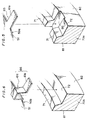
- Fig. 5 illustrates an anode buffer plate according to another preferred embodiment of the present invention.
- the anode buffer plate 50a have a plurality of arms 65, only one of which is shown in Fig. 5.
- Each arm 65 has a horizontal portion 61a only and respective notches of a gate ring 70a have the horizontal channels 95 only.
- Fig. 6 shows another anode buffer plate 50b.
- Respective arms 66 of the anode buffer plate 50b have bridge portions 61c and horizontal portions 61d.
- the bridge portion 61c straddles a prejection 71 of a gate ring 70b.
- These arms 66 are used in combination with the gate ring 70b having on notch.
- the ends of the horizontal portions 61a and 61d extend to the place very near the inner wall surface 10a of the insulating cylinder 10 shown in Fig. 1B.
- Fig. 7 is a plane view of an anode buffer plate 110 having three arms 112-114.
- the arms 112-114 are disposed at equal intervals on the circumference of a circular central portion 111.
- Each of the arms 112-114 may be the same as the arm 61 as shown in Fig. 3, or may be the same as either of the arms 65 and 66 as shown in Fig. 5 and Fig. 6.
- two dimensional positioning of the anode buffer plate is always attained.
- An anode buffer plate 120 of Fig. 8A has two arms 122 and 123 aligned across the diameter of a central portion 121.
- the direction of mutually connecting the arms 122 and 123 is denoted as X
- displacement of the anode buffer plate. 120 in the direction X is prevented by the arms 122 and 123.
- the respective widths W of the arms 122 and 123 are made relatively large, only a slight displacement of the anode buffer plate 120 in the direction Y causes the ends of the arms 122 and 123 to be in direct contact with the inner wall surface 10a of the insulating cylinder 10, as shown in a broken arrow 130 in Fig. 8B.
- the number of the arms in an anode buffer plate is not limited and an anode buffer plate having an arbitrary number of arms can be employed.
- the semiconductor devices to which the present invention is applicable are not limited to the gate turn-off thyristor.
- the present invention is applicable for example to other thyristors and transistors, and also to the elements having no control electrode such as diodes.
- the present invention is applicable to the cathode buffer plate.
- An advantage of the invention is that an electrode buffer plate is provided with at least one arm, so that displacement of the electrode buffer plate over a passing over the guide ring can be effectively prevented.
- displacement of the electrode buffer plate can be effectively prevented by inserting the end portion of the arm into the gap between the guide ring and an insulating cylinder.
Landscapes
- Thyristors (AREA)
- Die Bonding (AREA)
Claims (16)
- Hochleistungs-Halbleiterbauelement, das aufweist:(a) ein Halbleiterelement mit:(a-1) einem Halbleitersubstrat (3) mit einer oberen und einer unteren Hauptfläche;(a-2) einer ersten Elektrode (2), die auf der oberen Hauptfläche vorgesehen ist, wobei die erste Elektrode in Form einer scheibenförmigen Verstärkungsplatte ist; und(a-3) einer zweiten Elektrode (4), die auf der unteren Hauptfläche vorgesehen ist;(b) einer Elektrodenpufferplatte (50, 110, 120), die auf der ersten Elektrode (2) vorgesehen und damit in Kontakt ist;(c) einem ersten Elektrodenleiter (8), der auf der Elektrodenpufferplatte (50, 110, 120) vorgesehen und damit in Kontakt ist;(d) einem zweiten Elektrodenleiter (22), der auf der zweiten Elektrode (4) vorgesehen und elektrisch damit verbunden ist;(e) einem isolierenden Führungsring (70), in den das Halbleiterelement eingesetzt ist und der eine Position des Halbleiterelements begrenzt, wobei der isolierende Führungsring (70) einen Innendurchmesser hat, der dem Durchmesser der ersten Elektrode (2) im wesentlichen gleich ist; und(f) einen Isolierzylinder (10), in den der Führungsring (70) eingesetzt ist und der mit dem ersten und dem zweiten Elektrodenleiter (8, 22) verbunden ist;
wobei die Elektrodenpufferplatte (50, 110, 120) aufweist:(b-1) einen zentralen Bereich (51, 111, 121) mit einem Durchmesser, der an einen Innendurchmesser des Führungsrings (70) angepaßt ist; und(b-2) mindestens einen Arm (61-66, 112-114, 122, 123), der sich von dem zentralen Bereich (51, 111, 121) in eine Nähe einer Innenwandfläche (10a) des Isolierzylinders (10) erstreckt, wobei der Arm auf der oberen Oberfläche (83) des isolierenden Führungsrings (70) ruht. - Halbleiterbauelement nach Anspruch 1, wobei
die obere Endfläche (83) des Führungsrings (70) folgendes hat:
einen flachen Bereich, der eine obere Öffnung des Führungsrings umgibt; und
einen konvexen Bereich, der von dem flachen Bereich vorspringt und die obere Öffnung des Führungsrings umgibt, wobei der flache Bereich an einer Außenflächenseite des Führungsrings und der konvexe Bereich an einer Innenflächenseite des Führungsrings positioniert ist; und
der Arm den konvexen und den flachen Bereich kreuzt. - Halbleiterbauelement nach Anspruch 2, wobei
die obere Endfläche des Führungsrings ferner folgendes hat:
eine Kerbe, die über den konvexen Bereich gebildet ist; und
der Arm folgendes hat:
einen ersten Bereich, der sich von dem zentralen Bereich erstreckt und in der Kerbe aufgenommen ist. - Halbleiterbauelement nach Anspruch 3, wobei
die obere Endfläche des Führungsrings ferner folgendes hat:
einen Kanal, der über den flachen Bereich gebildet und mit der Kerbe ausgefluchtet ist; und
der erste Bereich des Arms ebenfalls in dem Kanal aufgenommen ist. - Halbleiterbauelement nach Anspruch 4, wobei
ein Spalt an einem Teil einer Grenzfläche zwischen dem Führungsring und dem Isolierzylinder vorgesehen ist, wobei der genannte Teil der Grenzfläche mit dem Kanal in Verbindung steht; und
der Arm ferner folgendes hat:
einen zweiten Bereich, der sich von dem ersten Bereich erstreckt und in den Spalt eingesetzt ist. - Halbleiterbauelement nach Anspruch 5, wobei
die Außenfläche des Führungsrings folgendes hat:
eine mit dem Kanal verbundene Ausnehmung, die als der Spalt dient. - Halbleiterbauelement nach Anspruch 6, wobei
der Arm an einer Grenzfläche zwischen dem ersten und dem zweiten Bereich hakenförmig ausgebildet ist. - Halbleiterbauelement nach Anspruch 2, wobei
der Arm folgendes hat:
einen Brückenbereich, der sich von dem zentralen Bereich erstreckt und den konvexen Bereich überspannt. - Halbleiterbauelement nach Anspruch 8, wobei
der Arm ferner folgendes hat:
einen geraden Bereich, der sich von dem Brückenbereich erstreckt und auf dem flachen Bereich der oberen Endfläche angeordnet ist. - Halbleiterbauelement nach Anspruch 1, wobei
die Elektrodenpufferplatte eine Vielzahl von Armen hat, deren Form jeweils dem genannten Arm entspricht. - Halbleiterbauelement nach Anspruch 10, wobei
die Vielzahl von Armen entlang einem Umfang des zentralen Bereichs in gleichen Abständen angeordnet ist. - Verfahren zum Herstellen eines Halbleiterbauelements, wobei ein Halbleiterelement zwischen einen ersten und einen zweiten Elektrodenleiter (8, 22) eingesetzt ist und das Halbleiterelement ein Halbleitersubstrat (3) mit einer oberen und einer unteren Hauptfläche aufweist, auf denen eine erste und eine zweite Elektrode (2, 4) vorgesehen sind, wobei die erste Elektrode (2) in Form einer scheibenförmigen Verstärkungsplatte ist, wobei das Verfahren die folgenden Schritte aufweist:(a) Bereitstellen eines Isolierzylinders (10) mit einer oberen und einer unteren Öffnung;(b) Bereitstellen einer Konstruktion, bei der der zweite Elektrodenleiter (22) in die untere Öffnung eingesetzt wird, der Isolierzylinder (10) mit dem zweiten Elektrodenleiter (22) verbunden wird und ein isolierender Führungsring (70) in einen Mittelbereich eines Raums eingesetzt wird, der von dem Isolierzylinder (10) umgeben ist;(c) Einführen des Halbleiterelements von der oberen Öffnung in den Raum, wobei die zweite Elektrode (4) dem zweiten Elektrodenleiter (22) zugewandt ist, um dadurch das Halbleiterelement in den isolierenden Führungsring (70) einzusetzen; wobei der isolierende Führungsring (70) einen Außendurchmesser, der dem Innendurchmesser des Isolierzylinders (10) im wesentlichen gleich ist, und einen Innendurchmesser hat, der dem Durchmesser der ersten Elektrode (2) im wesentlichen gleich ist;(d) Einführen einer Elektrodenpufferplatte (50) von der oberen Öffnung in den Raum und Anordnen der Elektrodenpufferplatte (50) auf dem Halbleiterelement, wobei die Elektrodenpufferplatte (50) aufweist: einen zentralen Bereich (51, 111, 121) mit einem Durchmesser, der einem Innendurchmesser des Führungsrings (70) entspricht; und
mindestens einen Arm (61-66, 112-114, 122, 123), der sich von dem zentralen Bereich erstreckt;(e) Anordnen des ersten Elektrodenleiters (8) auf der Elektrodenpufferplatte (50) durch die obere Öffnung hindurch; und(f) Verbinden des ersten Elektrodenleiters (8) mit dem Isolierzylinder (10);
wobei eine Größe des Arms derart festgelegt ist, daß der Arm eine Nähe einer Innenfläche (10a) des Isolierzylinders (10) erreicht, wenn die Elektrodenpufferplatte (50) in Schritt (d) auf dem Halbleiterelement angeordnet wird. - Verfahren nach Anspruch 12, wobei
der Führungsring eine obere Endfläche hat, die einen flachen Bereich, der eine obere Öffnung des Führungsrings umgibt, und einen konvexen Bereich hat, der von dem flachen Bereich vorspringt und die obere Öffnung des Führungsrings umgibt, wobei der flache Bereich an einer Außenflächenseite des Führungsrings und der konvexe Bereich an einer Innenflächenseite des Führungsrings positioniert ist; und
der Schritt (d) den folgenden Schritt aufweist:
(d-1) Positionieren des Arms über den flachen Bereich und den konvexen Bereich. - Verfahren nach Anspruch 13, wobei
eine Kerbe über den konvexen Bereich gebildet ist; und
der Schritt (d-1) den folgenden Schritt aufweist: Einsetzen des Arms in die Kerbe. - Verfahren nach Anspruch 14, wobei
ein Kanal, der mit der Kerbe ausgefluchtet ist, in dem flachen Bereich gebildet ist; und
der Schritt (d-1) den folgenden Schritt aufweist:
Einsetzen des Arms in die Kerbe und den Kanal. - Verfahren nach Anspruch 15, wobei
eine mit dem Kanal verbundene Ausnehmung in einer Außenfläche des Führungsrings gebildet ist;
der Arm einen ersten Bereich, der sich von dem zentralen Bereich erstreckt, und einen zweiten Bereich aufweist, der sich von dem ersten Bereich erstreckt und an einer Grenzfläche zwischen dem ersten und dem zweiten Bereich hakenförmig ausgebildet ist; und
der Schritt (d-1) den folgenden Schritt aufweist:
Einsetzen des zweiten Bereichs in die Ausnehmung unter gleichzeitigem Einsetzen des ersten Bereichs in die Kerbe und den Kanal.
Applications Claiming Priority (2)
| Application Number | Priority Date | Filing Date | Title |
|---|---|---|---|
| JP289005/89 | 1989-11-06 | ||
| JP1289005A JPH0760893B2 (ja) | 1989-11-06 | 1989-11-06 | 半導体装置およびその製造方法 |
Publications (3)
| Publication Number | Publication Date |
|---|---|
| EP0428044A2 EP0428044A2 (de) | 1991-05-22 |
| EP0428044A3 EP0428044A3 (en) | 1991-10-30 |
| EP0428044B1 true EP0428044B1 (de) | 1995-02-08 |
Family
ID=17737610
Family Applications (1)
| Application Number | Title | Priority Date | Filing Date |
|---|---|---|---|
| EP90121214A Expired - Lifetime EP0428044B1 (de) | 1989-11-06 | 1990-11-06 | Hochleistungshalbleiteranordnung mit Gehäuse |
Country Status (4)
| Country | Link |
|---|---|
| US (1) | US5121189A (de) |
| EP (1) | EP0428044B1 (de) |
| JP (1) | JPH0760893B2 (de) |
| DE (1) | DE69016748T2 (de) |
Families Citing this family (17)
| Publication number | Priority date | Publication date | Assignee | Title |
|---|---|---|---|---|
| JPH04352457A (ja) * | 1991-05-30 | 1992-12-07 | Mitsubishi Electric Corp | 圧接型半導体装置及びその製造方法 |
| US5371386A (en) * | 1992-04-28 | 1994-12-06 | Mitsubishi Denki Kabushiki Kaisha | Semiconductor device and method of assembling the same |
| DE4227063A1 (de) * | 1992-08-15 | 1994-02-17 | Abb Research Ltd | Abschaltbares Hochleistungs-Halbleiterbauelement |
| JP3471880B2 (ja) * | 1994-02-23 | 2003-12-02 | 三菱電機株式会社 | 圧接型半導体装置 |
| DE19505387A1 (de) * | 1995-02-17 | 1996-08-22 | Abb Management Ag | Druckkontaktgehäuse für Halbleiterbauelemente |
| JP3018971B2 (ja) * | 1995-12-18 | 2000-03-13 | 富士電機株式会社 | 半導体装置 |
| JP3571354B2 (ja) * | 1999-01-18 | 2004-09-29 | 三菱電機株式会社 | 圧接型半導体装置 |
| DE19903245A1 (de) * | 1999-01-27 | 2000-08-03 | Asea Brown Boveri | Leistungshalbleitermodul |
| US6445013B1 (en) * | 2000-04-13 | 2002-09-03 | Mitsubishi Denki Kabushiki Kaisha | Gate commutated turn-off semiconductor device |
| EP1291914A1 (de) * | 2001-09-10 | 2003-03-12 | ABB Schweiz AG | Druckkontaktierbares Leistungshalbleitermodul |
| US7132698B2 (en) * | 2002-01-25 | 2006-11-07 | International Rectifier Corporation | Compression assembled electronic package having a plastic molded insulation ring |
| JP5040234B2 (ja) * | 2006-09-26 | 2012-10-03 | 三菱電機株式会社 | 圧接型半導体装置 |
| CN102290353B (zh) * | 2011-07-05 | 2013-07-24 | 江苏捷捷微电子股份有限公司 | 一种可控硅芯片与钼片的烧结模具及其使用方法 |
| JP2015056487A (ja) * | 2013-09-11 | 2015-03-23 | 株式会社東芝 | 半導体装置 |
| JP2016062983A (ja) * | 2014-09-16 | 2016-04-25 | 株式会社東芝 | 半導体装置 |
| JP6359573B2 (ja) * | 2016-01-19 | 2018-07-18 | 株式会社東芝 | 半導体装置 |
| JP6585569B2 (ja) * | 2016-09-15 | 2019-10-02 | 株式会社東芝 | 半導体装置 |
Family Cites Families (16)
| Publication number | Priority date | Publication date | Assignee | Title |
|---|---|---|---|---|
| US3581160A (en) * | 1968-12-23 | 1971-05-25 | Gen Electric | Semiconductor rectifier assembly having high explosion rating |
| US4099201A (en) * | 1977-04-11 | 1978-07-04 | General Electric Company | Semiconductor rectifier assembly having an insulating material therein that evolves gases when exposed to an arc |
| CH630490A5 (de) * | 1978-06-30 | 1982-06-15 | Bbc Brown Boveri & Cie | Gehaeuse fuer ein halbleiter-hochleistungsbauelement. |
| SE429802B (sv) * | 1979-02-21 | 1983-09-26 | Asea Ab | Halvledaranordning innefattande en tetande ringformad kropp av en sulfonpolymer eller av polyfenylensulfid |
| DE2936780C2 (de) * | 1979-09-12 | 1985-02-07 | Licentia Patent-Verwaltungs-Gmbh, 6000 Frankfurt | Halbleiterbauelement |
| JPS6138199Y2 (de) * | 1980-08-29 | 1986-11-05 | ||
| JPS5745974A (en) * | 1980-09-03 | 1982-03-16 | Internatl Rectifier Corp Japan Ltd | Pressure contact type semiconductor device |
| DE3308661A1 (de) * | 1983-03-11 | 1984-09-20 | SEMIKRON Gesellschaft für Gleichrichterbau u. Elektronik mbH, 8500 Nürnberg | Halbleiterelement |
| JPS605564A (ja) * | 1983-06-23 | 1985-01-12 | Fuji Electric Corp Res & Dev Ltd | 半導体装置 |
| GB2162366B (en) * | 1984-07-24 | 1987-09-30 | Westinghouse Brake & Signal | Semiconductor device contact arrangements |
| JPS61136238A (ja) * | 1984-12-07 | 1986-06-24 | Hitachi Ltd | 半導体装置 |
| JPS61156768A (ja) * | 1984-12-27 | 1986-07-16 | Fuji Electric Co Ltd | 半導体装置 |
| JPS61260642A (ja) * | 1985-05-15 | 1986-11-18 | Toshiba Corp | 圧接型半導体装置 |
| JPH081914B2 (ja) * | 1987-03-31 | 1996-01-10 | 株式会社東芝 | 圧接型半導体装置 |
| JPH0693468B2 (ja) * | 1988-08-09 | 1994-11-16 | 株式会社東芝 | 圧接平型半導体装置 |
| US4956696A (en) * | 1989-08-24 | 1990-09-11 | Sundstrand Corporation | Compression loaded semiconductor device |
-
1989
- 1989-11-06 JP JP1289005A patent/JPH0760893B2/ja not_active Expired - Fee Related
-
1990
- 1990-10-30 US US07/605,277 patent/US5121189A/en not_active Expired - Fee Related
- 1990-11-06 EP EP90121214A patent/EP0428044B1/de not_active Expired - Lifetime
- 1990-11-06 DE DE69016748T patent/DE69016748T2/de not_active Expired - Fee Related
Also Published As
| Publication number | Publication date |
|---|---|
| EP0428044A2 (de) | 1991-05-22 |
| DE69016748T2 (de) | 1995-06-08 |
| JPH03149880A (ja) | 1991-06-26 |
| EP0428044A3 (en) | 1991-10-30 |
| US5121189A (en) | 1992-06-09 |
| JPH0760893B2 (ja) | 1995-06-28 |
| DE69016748D1 (de) | 1995-03-23 |
Similar Documents
| Publication | Publication Date | Title |
|---|---|---|
| EP0428044B1 (de) | Hochleistungshalbleiteranordnung mit Gehäuse | |
| US5278434A (en) | Pressure engagement structure for a full press-pack type semiconductor device | |
| JP3256636B2 (ja) | 圧接型半導体装置 | |
| JP7422799B2 (ja) | パワー半導体デバイス、パッケージ構造および電子デバイス | |
| US4107727A (en) | Resin sealed semiconductor device | |
| GB2039144A (en) | Semiconductor housing | |
| US5990501A (en) | Multichip press-contact type semiconductor device | |
| EP0194946B1 (de) | Statischer Induktionsthyristor mit Doppel-Gate vom Druckkontakttyp | |
| US5726466A (en) | Press pack power semiconductor device incorporating a plurality of semiconductor elements | |
| US5043795A (en) | Semiconductor device | |
| EP0421344B1 (de) | Leistungshalbleiteranordnung vom Drucktyp | |
| US3599057A (en) | Semiconductor device with a resilient lead construction | |
| EP0067575B1 (de) | Leistungshalbleiteranordnung | |
| US4672417A (en) | Semiconductor apparatus | |
| EP1049175B1 (de) | Rückwärtsleitender thyristor, halbleiteranordnung mit mechanischem kontakt und halbleitersubstrat | |
| JP7621445B2 (ja) | パワーモジュール | |
| JP4035447B2 (ja) | 半導体装置およびその製造方法 | |
| US5148254A (en) | Finely controlled semiconductor device | |
| EP0244767A2 (de) | Hermetisches Halbleitergehäuse und Verfahren zum Herstellen | |
| US12488995B2 (en) | Manufacturing method of insert case for semiconductor device and semiconductor device | |
| US3368122A (en) | Semiconductor devices | |
| US5796123A (en) | Semiconductor component mounted by brazing | |
| US6339231B1 (en) | Gate commutated turn-off thyristor module | |
| US3204023A (en) | Semiconductor device header with semiconductor support | |
| EP0660396A1 (de) | Leistungsanordnung von MOS-Chip-Typ und Packungszusammenbau |
Legal Events
| Date | Code | Title | Description |
|---|---|---|---|
| PUAI | Public reference made under article 153(3) epc to a published international application that has entered the european phase |
Free format text: ORIGINAL CODE: 0009012 |
|
| 17P | Request for examination filed |
Effective date: 19901212 |
|
| AK | Designated contracting states |
Kind code of ref document: A2 Designated state(s): CH DE FR GB LI |
|
| PUAL | Search report despatched |
Free format text: ORIGINAL CODE: 0009013 |
|
| AK | Designated contracting states |
Kind code of ref document: A3 Designated state(s): CH DE FR GB LI |
|
| 17Q | First examination report despatched |
Effective date: 19930813 |
|
| GRAA | (expected) grant |
Free format text: ORIGINAL CODE: 0009210 |
|
| AK | Designated contracting states |
Kind code of ref document: B1 Designated state(s): CH DE FR GB LI |
|
| REF | Corresponds to: |
Ref document number: 69016748 Country of ref document: DE Date of ref document: 19950323 |
|
| ET | Fr: translation filed | ||
| REG | Reference to a national code |
Ref country code: GB Ref legal event code: 746 Effective date: 19951026 |
|
| PLBE | No opposition filed within time limit |
Free format text: ORIGINAL CODE: 0009261 |
|
| STAA | Information on the status of an ep patent application or granted ep patent |
Free format text: STATUS: NO OPPOSITION FILED WITHIN TIME LIMIT |
|
| 26N | No opposition filed | ||
| REG | Reference to a national code |
Ref country code: FR Ref legal event code: D6 |
|
| PGFP | Annual fee paid to national office [announced via postgrant information from national office to epo] |
Ref country code: GB Payment date: 20011107 Year of fee payment: 12 |
|
| PGFP | Annual fee paid to national office [announced via postgrant information from national office to epo] |
Ref country code: FR Payment date: 20011113 Year of fee payment: 12 |
|
| PGFP | Annual fee paid to national office [announced via postgrant information from national office to epo] |
Ref country code: DE Payment date: 20011119 Year of fee payment: 12 |
|
| PGFP | Annual fee paid to national office [announced via postgrant information from national office to epo] |
Ref country code: CH Payment date: 20011130 Year of fee payment: 12 |
|
| REG | Reference to a national code |
Ref country code: GB Ref legal event code: IF02 |
|
| PG25 | Lapsed in a contracting state [announced via postgrant information from national office to epo] |
Ref country code: GB Free format text: LAPSE BECAUSE OF NON-PAYMENT OF DUE FEES Effective date: 20021106 |
|
| PG25 | Lapsed in a contracting state [announced via postgrant information from national office to epo] |
Ref country code: LI Free format text: LAPSE BECAUSE OF NON-PAYMENT OF DUE FEES Effective date: 20021130 Ref country code: CH Free format text: LAPSE BECAUSE OF NON-PAYMENT OF DUE FEES Effective date: 20021130 |
|
| PG25 | Lapsed in a contracting state [announced via postgrant information from national office to epo] |
Ref country code: DE Free format text: LAPSE BECAUSE OF NON-PAYMENT OF DUE FEES Effective date: 20030603 |
|
| GBPC | Gb: european patent ceased through non-payment of renewal fee | ||
| REG | Reference to a national code |
Ref country code: CH Ref legal event code: PL |
|
| PG25 | Lapsed in a contracting state [announced via postgrant information from national office to epo] |
Ref country code: FR Free format text: LAPSE BECAUSE OF NON-PAYMENT OF DUE FEES Effective date: 20030731 |
|
| REG | Reference to a national code |
Ref country code: FR Ref legal event code: ST |