EP0428067A2 - Integrierter Halbleiterschaltkreis und Methode zu seiner Herstellung - Google Patents
Integrierter Halbleiterschaltkreis und Methode zu seiner Herstellung Download PDFInfo
- Publication number
- EP0428067A2 EP0428067A2 EP90121380A EP90121380A EP0428067A2 EP 0428067 A2 EP0428067 A2 EP 0428067A2 EP 90121380 A EP90121380 A EP 90121380A EP 90121380 A EP90121380 A EP 90121380A EP 0428067 A2 EP0428067 A2 EP 0428067A2
- Authority
- EP
- European Patent Office
- Prior art keywords
- layer
- type
- forming
- concentration
- circuit
- Prior art date
- Legal status (The legal status is an assumption and is not a legal conclusion. Google has not performed a legal analysis and makes no representation as to the accuracy of the status listed.)
- Withdrawn
Links
Images


Classifications
-
- H—ELECTRICITY
- H10—SEMICONDUCTOR DEVICES; ELECTRIC SOLID-STATE DEVICES NOT OTHERWISE PROVIDED FOR
- H10D—INORGANIC ELECTRIC SEMICONDUCTOR DEVICES
- H10D10/00—Bipolar junction transistors [BJT]
-
- H—ELECTRICITY
- H10—SEMICONDUCTOR DEVICES; ELECTRIC SOLID-STATE DEVICES NOT OTHERWISE PROVIDED FOR
- H10D—INORGANIC ELECTRIC SEMICONDUCTOR DEVICES
- H10D84/00—Integrated devices formed in or on semiconductor substrates that comprise only semiconducting layers, e.g. on Si wafers or on GaAs-on-Si wafers
- H10D84/01—Manufacture or treatment
- H10D84/0107—Integrating at least one component covered by H10D12/00 or H10D30/00 with at least one component covered by H10D8/00, H10D10/00 or H10D18/00, e.g. integrating IGFETs with BJTs
- H10D84/0109—Integrating at least one component covered by H10D12/00 or H10D30/00 with at least one component covered by H10D8/00, H10D10/00 or H10D18/00, e.g. integrating IGFETs with BJTs the at least one component covered by H10D12/00 or H10D30/00 being a MOS device
-
- H—ELECTRICITY
- H10—SEMICONDUCTOR DEVICES; ELECTRIC SOLID-STATE DEVICES NOT OTHERWISE PROVIDED FOR
- H10D—INORGANIC ELECTRIC SEMICONDUCTOR DEVICES
- H10D84/00—Integrated devices formed in or on semiconductor substrates that comprise only semiconducting layers, e.g. on Si wafers or on GaAs-on-Si wafers
- H10D84/01—Manufacture or treatment
- H10D84/02—Manufacture or treatment characterised by using material-based technologies
- H10D84/03—Manufacture or treatment characterised by using material-based technologies using Group IV technology, e.g. silicon technology or silicon-carbide [SiC] technology
- H10D84/038—Manufacture or treatment characterised by using material-based technologies using Group IV technology, e.g. silicon technology or silicon-carbide [SiC] technology using silicon technology, e.g. SiGe
-
- H—ELECTRICITY
- H10—SEMICONDUCTOR DEVICES; ELECTRIC SOLID-STATE DEVICES NOT OTHERWISE PROVIDED FOR
- H10D—INORGANIC ELECTRIC SEMICONDUCTOR DEVICES
- H10D84/00—Integrated devices formed in or on semiconductor substrates that comprise only semiconducting layers, e.g. on Si wafers or on GaAs-on-Si wafers
- H10D84/40—Integrated devices formed in or on semiconductor substrates that comprise only semiconducting layers, e.g. on Si wafers or on GaAs-on-Si wafers characterised by the integration of at least one component covered by groups H10D12/00 or H10D30/00 with at least one component covered by groups H10D10/00 or H10D18/00, e.g. integration of IGFETs with BJTs
- H10D84/401—Combinations of FETs or IGBTs with BJTs
Definitions
- the present invention relates generally to a semiconductor integrated circuit and a method of manufacturing the same, and in particularly to a bi-CMOS type semiconductor integrated circuit wherein a bipolar transistor and an insulated gate type complementary MOS transistor are integrated on a single chip, and a method of manufacturing this integrated circuit.
- CMOS complementary metal-oxide-semiconductor
- CMOS complementary metal-oxide-semiconductor
- the following patterning techniques have been conventionally adopted: to provide a power line and a ground line separately for the bipolar circuit and for the CMOS circuit, or to separate both circuits sufficiently.
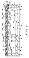
- Fig. 1 shows a cross-sectional structure of a conventional Bi-CMOS integrated circuit.
- Reference numeral 31 denotes a P-type silicon substrate; 321 and 322 N+ buried layers; 33 a P-type epitaxial layer; 341 a a first N-well diffusion layer, formed within the epitaxial layer 33 and on the N+ buried layer 321, for the formation of a P-channel MOS transistor; 342 a second N-well diffusion layer, formed within the epitaxial layer 33 and on the N+ buried layer 322, for the formation of an NPN transistor; 35 a deep N+ diffusion layer extending from the surface of the second N-well diffusion layer 342 to the N+ buried layer 322; 36 an element isolation region (field oxide film); 37 a gate oxide film; 38 a gate electrode of the P-channel MOS transistor; 39 a gate electrode of an N-channel MOS transistor; 40 an internal base region (P- diffusion layer) of the NPN transistor; 411 and 422 a drain region and
- the present invention has been devised in consideration of the above problem, and its object is to provide a semiconductor integrated circuit and a method of manufacturing the same, wherein noise occurring in a CMOS circuit is prevented from adversely affecting a bipolar circuit, and the manufacture of the circuit is relatively easy, and the number of manufacturing processes can be reduced.
- the present invention provides a semiconductor integrated circuit wherein a bipolar transistor and an insulated gate type complementary transistor are formed on a single semiconductor chip, characterized in that said insulated gate type complementary transistor is formed in an island-shaped epitaxial layer which is completely isolated from a semiconductor substrate and the other part of the circuit and which has a conductivity type opposite to that of the semiconductor substrate, and that an electrode is formed in contact with a region for isolating said island-shaped epitaxial layer from the other part of the circuit.
- this invention provides a method of manufacturing a semiconductor integrated circuit wherein a bipolar transistor and an insulated gate type complementary transistor are formed on a single semiconductor chip, said method comprising the steps of: forming an island portion in an epitaxial layer formed in a surface portion of a semiconductor substrate and having a conductivity type opposite to that of the semiconductor substrate, said island portion being isolated completely from the semiconductor substrate and the other part of the circuit; forming an insulated gate type complementary transistor in said isalnd portion in the epitaxial layer; and forming an electrode in contact with a region for isolating said island portion from the other part of the circuit.
- the CMOS circuit is formed in the island-shaped epitaxial layer isolated completely from the semiconductor substrate and the other part of the circuit.
- noise occurring in the CMOS circuit does not adversely affect the bipolar circuit.
- the operation margin of the semiconductor integrated circuit is increased, the malfunction of the circuit can be prevented.
- the integration density can be increased and the number of external pins can be reduced.
- the electrode is formed in contact with the region for isolating the island-shaped epitaxial layer of the CMOS transistor region from the other part, the potential of the island-shaped epitaxial layer can be determined independently from that of the other part, by applying a desired potential to the electrode.
- the semiconductor integrated circuit having the above features can be manufactured by the combination of the well-known processes.
- Figs. 2A to 2C illustrate an example of a process of manufacturing a Bi-CMOS integrated circuit according to an embodiment of the present invention.
- a P-type silicon substrate 1 with about 25 Q.cm is oxidized at a temperature of 1000°C, thereby forming an oxide film (not shown) with a thickness of about 0.8 ⁇ on the substrate 1.
- the resultant structure is subjected to a photoetching process (PEP), thus removing part of the oxide film.
- PEP photoetching process
- PEP photoetching process
- Sb antimony
- the oxide film is removed, and an oxide film (not shown) with a thickness of 1000 ⁇ is formed under an oxidation treatment at a temperature of 1000°C. Thereafter, using a photoresist pattern as a mask, boron (B) ions are implanted to form P+ buried layers 3 on part of the second N+ buried layer 22 and between the N+ buried layers 21 and 22. Then, the oxide film is removed, and phosphorus (P) doped N-type epitaxial layers 4 are grown on the substrate. In this case, the resistivity ⁇ VG of each epitaxial layer 4 is set to about 1.5 ⁇ .cm, and the thickness tVG thereof is set to about 3 ⁇ m.
- an oxide film (not shown) with a thickness of 500 ⁇ is formed by an oxidation treatment at a temperature of 1000°C.
- boron ions are implanted in a predetermined area
- phosphorus ions are implanted in a predetermined area.
- the oxide film is removed and an undoped CVD oxide film having a thickness of about 3000 ⁇ is formed on the substrate by means of CVD (chemical vapor deposition). Then, a thermal diffusion treatment is carried out at a temperature of 1150°C.
- a P-well diffusion layer 5 extending to the P+ buried layer 3, a first deep N+ diffusion layer 61 extending to the first deep N+ buried layer 21, and a second deep N+ diffusion layer 62 extending to the second N+ buried layer and surrounding the CMOS transistor region are formed.
- the CVD oxide film is removed, and an oxidation treatment is performed at a temperature of 1000°C to form an oxide film (not shown) with a thickness of about 900 ⁇ and subsequently a silicon nitride film (not shown) with a thickness of about 2000 ⁇ is formed thereon. That portion of the silicon nitride film, which is not located on the activation region, is removed.
- a photoresist pattern for the formation of an element isolation region as a mask, a P ⁇ field inversion preventing layer 7 and an N ⁇ field inversion preventing layer 8 are formed, as shown in Fig. 2B.
- a field oxide film (SiO2 film) 9 with a thickness of 9000 ⁇ is formed (not shown) with the thickness of 900 ⁇ and the silicon nitride film (not shown) are removed, and a thin oxide film (SiO2 film) 11 having a thickness of about 400 ⁇ , part of which serves as a gate oxide film 10, is formed by a heat treatment at 950°C.
- An undoped polycrystalline silicon (“polysilicon”) film with a thickness of 4000 ⁇ is formed on the resultant structure by means of CVD. Phosphorus is diffused at 950°C, and the polysilicon film is rendered N+ conductive.
- the polysilicon film is patterned by means of PEP and reactive ion etching (RIE), thereby forming a gate electrode 111 of the P-channel MOS transistor and a gate electrode 112 of the N-channel MOS transistor.
- RIE reactive ion etching
- boron ions are implanted to form a P ⁇ diffusion layer 12 corresponding to an internal base region of the NPN transistor.
- the thin oxide film is selectively removed and arsenic ions (As) ions are implanted thereby forming a drain region 131 and a source region (N+ region) 132 of the N-channel MOS transistor.
- the photoresist is removed and an oxidation treatment is performed at 900°C to form a thermal oxidation film (not shown).
- boron ions are implanted thereby forming a P+ diffusion layer 141 corresponding to the external base region of the NPN transistor, and a drain region 1421 and a source region (P+ region) 1422 of the P-channel MOS transistor, as is shown in Fig. 2C.
- arsenic (As) ions are implanted to form an N+ diffusion layer 15 in the emitter region of the NPN transistor.
- An undoped CVD oxide film and a boron-phosphor-silicated glass (BPSG) film are successively formed as an interlayer insulating film 16 by means of CVD. Then, melting and getter treatments are carried out at 950°C. Then, a contact region is formed by PEP, and, using the contact region as a mask, the interlayer insulating film 16 (BPSG film and undoped CVD oxide film) is etched by RIE, thereby forming an electrode contact hole.
- an aluminum-silicon (Al-Si) layer with a thickness of, e.g. 8000 ⁇ is formed by means of sputtering.
- This layer is patterned, thereby forming an emitter electrode 171 in contact with the emitter region 15 (N+ diffusion layer) of the NPN transistor; a base electrode 172 in contact with the base region (P+ diffusion layer) 141 of the NPN transistor; a collector electrode 173 in contact with the first deep N+ diffusion layer 61; a drain electrode 1741 and a source electrode 1742, respectively in contact with the drain region 1421 and source region 1422 (N+ region) of the P-channel MOS transistor; a drain electrode 1751 and a source electrode 1752, respectively in contact with the drain region 131 and source region 132 (N+ region) of the N-channel MOS transistor; and an electrode 176 in contact with the second deep N+ diffusion layer 62 surrounding the CMOS region.
- a forming treatment is carried out at a temperature of 450°C to obtain desired characteristics.
- a surface protection film (not shown) is formed by means of CVD, and a bonding pad formation region is formed by means of PEP.
- the manufacturing process is completed.
- the CMOS transistor is formed in the island-shaped N-epitaxial layer and P-well region, which is isolated from the remaining part of the semiconductor substrate.
- noise occurring in the CMOS circuit does not adversely affect the bipolar circuit.
- the operation margin of the semiconductor integrated circuit increases and the malfunction is prevented.
- it is not necessary to make a special patterning e.g. providing the power line and ground line separately for the bipolar circuit and the CMOS circuit, or separating both circuits with a sufficient distance.
- integration density can be increased, and the number of external pins can be decreased.
- an electrode is put in contact with the region for isolating the islandshaped CMOS transistor region from the remaining part.
- the substrate potential of the island-shaped CMOS transistor region can be determined independently from the substrat potential of the other part.
- this device is relatively simple, and the number of manufacturing steps can be reduced, compared to the conventional Bi-CMOS integrated circuit.
- Fig. 3 is a cross-sectional view showing a structure of a Bi-CMOS integrated circuit according to another embodiment of the invention.
- This circuit differs from the circuit of Fig. 2C, only in that the second depp N+ diffusion layer 62 is replaced by an N-well diffusion layer 18 and an N+ diffusion layer 19 formed on the surface region of the layer 18.
- the structural elements already shown in Fig. 2C are denoted by the same reference numerals.
- the method of manufacturing the Bi-CMOS integrated circuit of Fig. 3 differs from that of manufacturing the circuit of Fig.
- step of forming the second deep N+ diffusion layer 62 is replaced by the step of forming the N-well diffusion layer 18, and the N+ diffusion layer 19 is formed at the time of forming the drain region 131 and source region 132 (N+ diffusion layer) of the N-channel transistor.
- an island-shaped N-epitaxial layer is formed such that an island-shaped CMOS transistor region is isolated from the semiconductor subtrate and the other part.
- noise occurring in the CMOS circuit does not adversely affect the bipolar circuit.
- the operation margin of the semiconductor integrated circuit is increased, the malfunction of the circuit can be prevented.
- it is not necessary to make special patterning e.g. to provide the power line and ground line separately for the bipolar circuit and the CMOS circuit, or to separate both circuits with a sufficient distance.
- the integration density can be increased and the number of external pins can be reduced.
- the electrode is formed in contact with the region for isolating the island-shaped CMOS transistor region from the other part, the substrate potential of the island-shaped CMOS transistor region can be determined independently from that of the other part.
- the semiconductor integrated circuit having the above features can be manufactured by the combination of the well-known processes.
Landscapes
- Metal-Oxide And Bipolar Metal-Oxide Semiconductor Integrated Circuits (AREA)
Applications Claiming Priority (2)
| Application Number | Priority Date | Filing Date | Title |
|---|---|---|---|
| JP1291206A JPH0744231B2 (ja) | 1989-11-10 | 1989-11-10 | 半導体集積回路およびその製造方法 |
| JP291206/89 | 1989-11-10 |
Publications (2)
| Publication Number | Publication Date |
|---|---|
| EP0428067A2 true EP0428067A2 (de) | 1991-05-22 |
| EP0428067A3 EP0428067A3 (en) | 1992-05-13 |
Family
ID=17765834
Family Applications (1)
| Application Number | Title | Priority Date | Filing Date |
|---|---|---|---|
| EP19900121380 Withdrawn EP0428067A3 (en) | 1989-11-10 | 1990-11-08 | Semiconductor integrated circuit and method of manufacturing the same |
Country Status (3)
| Country | Link |
|---|---|
| EP (1) | EP0428067A3 (de) |
| JP (1) | JPH0744231B2 (de) |
| KR (1) | KR910010734A (de) |
Cited By (2)
| Publication number | Priority date | Publication date | Assignee | Title |
|---|---|---|---|---|
| WO1995023430A1 (en) * | 1994-02-28 | 1995-08-31 | National Semiconductor Corporation | Bipolar and bicmos structures and methods of fabrication |
| EP0782192A1 (de) * | 1995-12-30 | 1997-07-02 | Samsung Electronics Co., Ltd. | Elektrostatische Entladungsstruktur für eine Halbleiteranordnung |
Families Citing this family (1)
| Publication number | Priority date | Publication date | Assignee | Title |
|---|---|---|---|---|
| JP2825038B2 (ja) * | 1992-02-27 | 1998-11-18 | 日本電気株式会社 | 半導体装置 |
Family Cites Families (5)
| Publication number | Priority date | Publication date | Assignee | Title |
|---|---|---|---|---|
| JPS5885558A (ja) * | 1981-11-17 | 1983-05-21 | Olympus Optical Co Ltd | セミカスタム半導体装置 |
| JPH0671067B2 (ja) * | 1985-11-20 | 1994-09-07 | 株式会社日立製作所 | 半導体装置 |
| JP2523506B2 (ja) * | 1986-06-25 | 1996-08-14 | 株式会社日立製作所 | 半導体装置 |
| JPS63293972A (ja) * | 1987-05-27 | 1988-11-30 | Hitachi Ltd | 半導体装置の製造方法 |
| US4825275A (en) * | 1987-05-28 | 1989-04-25 | Texas Instruments Incorporated | Integrated bipolar-CMOS circuit isolation for providing different backgate and substrate bias |
-
1989
- 1989-11-10 JP JP1291206A patent/JPH0744231B2/ja not_active Expired - Fee Related
-
1990
- 1990-11-08 KR KR1019900018011A patent/KR910010734A/ko not_active Abandoned
- 1990-11-08 EP EP19900121380 patent/EP0428067A3/en not_active Withdrawn
Cited By (5)
| Publication number | Priority date | Publication date | Assignee | Title |
|---|---|---|---|---|
| WO1995023430A1 (en) * | 1994-02-28 | 1995-08-31 | National Semiconductor Corporation | Bipolar and bicmos structures and methods of fabrication |
| US5543653A (en) * | 1994-02-28 | 1996-08-06 | National Semiconductor Corporation | Bipolar and BiCMOS structures |
| US5580798A (en) * | 1994-02-28 | 1996-12-03 | National Semiconductor Corporation | Method of fabricating bipolar transistor having a guard ring |
| EP0782192A1 (de) * | 1995-12-30 | 1997-07-02 | Samsung Electronics Co., Ltd. | Elektrostatische Entladungsstruktur für eine Halbleiteranordnung |
| US5760446A (en) * | 1995-12-30 | 1998-06-02 | Samsung Electronics Co., Ltd. | Electrostatic discharge structure of semiconductor device |
Also Published As
| Publication number | Publication date |
|---|---|
| KR910010734A (ko) | 1991-06-29 |
| JPH0744231B2 (ja) | 1995-05-15 |
| JPH03153069A (ja) | 1991-07-01 |
| EP0428067A3 (en) | 1992-05-13 |
Similar Documents
| Publication | Publication Date | Title |
|---|---|---|
| US4484388A (en) | Method for manufacturing semiconductor Bi-CMOS device | |
| US5065208A (en) | Integrated bipolar and CMOS transistor with titanium nitride interconnections | |
| EP0052450B1 (de) | Verfahren zur Herstellung eines Halbleiterbauelements mit polykristallinen Halbleiter- u. Metall-Elektroden | |
| EP0196757B1 (de) | Halbleiteranordnung mit einem bipolaren Transistor und einem MOS-Transistor und Verfahren zu deren Herstellung | |
| EP0219831A2 (de) | Verfahren zur Herstellung von integrierten Halbleiterschaltungen mit einem bipolaren Transistor und einem Feldeffekttransistor mit isolierter Steuerelektrode | |
| JPH05347383A (ja) | 集積回路の製法 | |
| EP0278619B1 (de) | Verfahren zum Herstellen integrierter Strukturen aus bipolaren und CMOS-Transistoren | |
| US5557131A (en) | Elevated emitter for double poly BICMOS devices | |
| US5319235A (en) | Monolithic IC formed of a CCD, CMOS and a bipolar element | |
| US4965216A (en) | Method of fabricating a bi-CMOS device | |
| US4735912A (en) | Process of fabricating a semiconductor IC device | |
| US5045493A (en) | Semiconductor device and method of manufacturing the same | |
| EP0438167B1 (de) | Halbleitervorrichtung mit Ladungstransfer-Bauelement, MOSFETs und Bipolartransistoren - alle in einem einzelnen Halbleitersubstrat gebildet | |
| JP2587444B2 (ja) | Cmos技術を用いたバイポーラ・トランジスタとその製造方法 | |
| EP0413256B1 (de) | Methode zur Herstellung einer Halbleiterstruktur für integrierte Hochleistungsschaltungen | |
| EP0743682A2 (de) | Integrierte Halbleiteranordnung mit Injektionslogik und Verfahren zu deren Herstellung | |
| US5288651A (en) | Method of making semiconductor integrated circuit device including bipolar transistors, MOS FETs and CCD | |
| US4464825A (en) | Process for fabrication of high-speed radiation hard bipolar semiconductor devices | |
| US6011283A (en) | Pillar emitter for BiCMOS devices | |
| EP0381139A2 (de) | Integrierte Halbleitervorrichtung und Verfahren zu ihrer Herstellung | |
| EP0428067A2 (de) | Integrierter Halbleiterschaltkreis und Methode zu seiner Herstellung | |
| EP0301468A2 (de) | Verfahren zum Herstellen komplementärer kontaktloser vertikaler Bipolartransistoren | |
| US4512076A (en) | Semiconductor device fabrication process | |
| EP0404180B1 (de) | Integrierte Halbleiterschaltung und Verfahren zu deren Herstellung | |
| KR940009356B1 (ko) | 반도체 집적회로장치 |
Legal Events
| Date | Code | Title | Description |
|---|---|---|---|
| PUAI | Public reference made under article 153(3) epc to a published international application that has entered the european phase |
Free format text: ORIGINAL CODE: 0009012 |
|
| 17P | Request for examination filed |
Effective date: 19901108 |
|
| AK | Designated contracting states |
Kind code of ref document: A2 Designated state(s): DE FR GB |
|
| PUAL | Search report despatched |
Free format text: ORIGINAL CODE: 0009013 |
|
| AK | Designated contracting states |
Kind code of ref document: A3 Designated state(s): DE FR GB |
|
| STAA | Information on the status of an ep patent application or granted ep patent |
Free format text: STATUS: THE APPLICATION HAS BEEN WITHDRAWN |
|
| 18W | Application withdrawn |
Withdrawal date: 19930915 |