EP0428377A2 - Convertisseur continu-continu à circuit de commutation - Google Patents
Convertisseur continu-continu à circuit de commutation Download PDFInfo
- Publication number
- EP0428377A2 EP0428377A2 EP90312367A EP90312367A EP0428377A2 EP 0428377 A2 EP0428377 A2 EP 0428377A2 EP 90312367 A EP90312367 A EP 90312367A EP 90312367 A EP90312367 A EP 90312367A EP 0428377 A2 EP0428377 A2 EP 0428377A2
- Authority
- EP
- European Patent Office
- Prior art keywords
- transformer
- converter circuit
- switching means
- diode
- terminal
- Prior art date
- Legal status (The legal status is an assumption and is not a legal conclusion. Google has not performed a legal analysis and makes no representation as to the accuracy of the status listed.)
- Granted
Links
Images



Classifications
-
- H—ELECTRICITY
- H05—ELECTRIC TECHNIQUES NOT OTHERWISE PROVIDED FOR
- H05B—ELECTRIC HEATING; ELECTRIC LIGHT SOURCES NOT OTHERWISE PROVIDED FOR; CIRCUIT ARRANGEMENTS FOR ELECTRIC LIGHT SOURCES, IN GENERAL
- H05B41/00—Circuit arrangements or apparatus for igniting or operating discharge lamps
-
- H—ELECTRICITY
- H02—GENERATION; CONVERSION OR DISTRIBUTION OF ELECTRIC POWER
- H02M—APPARATUS FOR CONVERSION BETWEEN AC AND AC, BETWEEN AC AND DC, OR BETWEEN DC AND DC, AND FOR USE WITH MAINS OR SIMILAR POWER SUPPLY SYSTEMS; CONVERSION OF DC OR AC INPUT POWER INTO SURGE OUTPUT POWER; CONTROL OR REGULATION THEREOF
- H02M3/00—Conversion of DC power input into DC power output
- H02M3/02—Conversion of DC power input into DC power output without intermediate conversion into AC
- H02M3/04—Conversion of DC power input into DC power output without intermediate conversion into AC by static converters
- H02M3/10—Conversion of DC power input into DC power output without intermediate conversion into AC by static converters using discharge tubes with control electrode or semiconductor devices with control electrode
- H02M3/145—Conversion of DC power input into DC power output without intermediate conversion into AC by static converters using discharge tubes with control electrode or semiconductor devices with control electrode using devices of a triode or transistor type requiring continuous application of a control signal
- H02M3/155—Conversion of DC power input into DC power output without intermediate conversion into AC by static converters using discharge tubes with control electrode or semiconductor devices with control electrode using devices of a triode or transistor type requiring continuous application of a control signal using semiconductor devices only
- H02M3/156—Conversion of DC power input into DC power output without intermediate conversion into AC by static converters using discharge tubes with control electrode or semiconductor devices with control electrode using devices of a triode or transistor type requiring continuous application of a control signal using semiconductor devices only with automatic control of output voltage or current, e.g. switching regulators
- H02M3/158—Conversion of DC power input into DC power output without intermediate conversion into AC by static converters using discharge tubes with control electrode or semiconductor devices with control electrode using devices of a triode or transistor type requiring continuous application of a control signal using semiconductor devices only with automatic control of output voltage or current, e.g. switching regulators including plural semiconductor devices as final control devices for a single load
-
- H—ELECTRICITY
- H02—GENERATION; CONVERSION OR DISTRIBUTION OF ELECTRIC POWER
- H02M—APPARATUS FOR CONVERSION BETWEEN AC AND AC, BETWEEN AC AND DC, OR BETWEEN DC AND DC, AND FOR USE WITH MAINS OR SIMILAR POWER SUPPLY SYSTEMS; CONVERSION OF DC OR AC INPUT POWER INTO SURGE OUTPUT POWER; CONTROL OR REGULATION THEREOF
- H02M3/00—Conversion of DC power input into DC power output
- H02M3/22—Conversion of DC power input into DC power output with intermediate conversion into AC
- H02M3/24—Conversion of DC power input into DC power output with intermediate conversion into AC by static converters
- H02M3/28—Conversion of DC power input into DC power output with intermediate conversion into AC by static converters using discharge tubes with control electrode or semiconductor devices with control electrode to produce the intermediate AC
- H02M3/325—Conversion of DC power input into DC power output with intermediate conversion into AC by static converters using discharge tubes with control electrode or semiconductor devices with control electrode to produce the intermediate AC using devices of a triode or a transistor type requiring continuous application of a control signal
- H02M3/335—Conversion of DC power input into DC power output with intermediate conversion into AC by static converters using discharge tubes with control electrode or semiconductor devices with control electrode to produce the intermediate AC using devices of a triode or a transistor type requiring continuous application of a control signal using semiconductor devices only
- H02M3/33569—Conversion of DC power input into DC power output with intermediate conversion into AC by static converters using discharge tubes with control electrode or semiconductor devices with control electrode to produce the intermediate AC using devices of a triode or a transistor type requiring continuous application of a control signal using semiconductor devices only having several active switching elements
Definitions
- This invention relates to DC/DC switching converter circuits such as are used in DC/DC and AC/DC power supplies, and more particularly to single ended DC/DC switching converter circuits.
- Single ended DC/DC converters are commonly classified as one of three classical topologies: the boost; the buck; and the buck-boost. These converters comprise various arrangements of a switch, a diode, an inductor and two capacitors. Dual circuits of these topologies also exist wherein two inductors and one capacitor appear.
- FIG. 1 illustrates a non-isolated, single switch buck-booster converter having a MOSFET power transistor Q1, inductor L1, diode D1, and capacitors C1 and C3.
- Fig. 1A illustrates the dual circuit of the buck-boost converter wherein shunt capacitors C1 and C3 are replaced by series inductors L2 and L3, shunt inductor L1 by series capacitor C2, and series switch Q1 by shunt switch Q2.
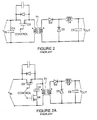
- Fig. 2 illustrates an isolated, single switch forward converter having transistor Q3, capacitors C4 and C5, diodes D2 and D3, inductor L4 and transformer T1.
- Fig. 2A illustrates a forward converter with a second flux reset switch Q4 and capacitor C4.
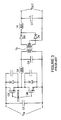
- FIG. 3 illustrates a full wave series resonant converter wherein the output is controlled by varying the switching frequency.
- the resonant converter shown includes transistors Q5 and Q6, capacitors C5, C6, and C7, diodes D5 and D6, inductors L5 and L6, and transformer T5.
- resonant converters can exhibit either zero current or zero voltage switching, thereby significantly reducing the switching loss.
- the reactive components must handle considerable power, sometimes amounting to several times the output power of the converter. This energy, which circulates through the components, can induce new losses which are greater than the decrease in switching loss.
- the operating voltage and/or RMS current stress on the semiconductor devices is often increased.
- a DC/DC converter allows zero-voltage switching while maintaining the beneficial features of the basic topologies and avoiding the disadvantages relating to resonant converter schemes.
- the invention may be embodied in a non-isolated form, an isolated form, an integrated magnetic form, and a coupled magnetic form.
- the non-isolated form comprises two switches, two diodes, two inductors, and at least one capacitor.
- the isolated form comprises two switches, two diodes, a transformer, an inductor, and at least one capacitor.
- the integrated magnetic form combines the transformer and the inductor of the isolated form on a common core with no mutual coupling.
- the coupled magnetic form introduces magnetic reluctance in the common flux paths of the integrated magnetic elements causing the output ripple current to be greatly reduced.
- An additional embodiment of the invention includes a transformer having a plurality of secondary windings. Each of the secondary windings is connected to output circuitry which includes a plurality of output lines where each output line provides an output DC voltage.
- energy stored in the magnetic elements is transferred to discharge the capacitance across each switch prior to closing the switch. Since the voltage across each switch is approximately zero as it is closed, switching loss is minimized. Hence, high converting efficiency may be realized.
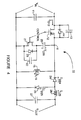
- a zero voltage switching converter 10 is shown in Figure 4.
- a capacitor 11 is connected across input terminals of converter 10 which receive a DC voltage.
- a transistor 12 switches input power to the remainder of converter 10 in response to a control signal.
- transistor 12 is a power MOSFET characterized with an intrinsic capacitance 13 and an intrinsic body diode 14 shunted across the source and drain of transistor 12.
- Capacitance 13 also includes any discrete lumped capacitance or stay capacitance across transistor 12.
- diode 14 may be a discrete device rather than an intrinsic body diode of transistor 12.
- An inductor 15 is connected to the drain of transistor 12 and receives input power when transistor 12 is "on”.
- a capacitor 20 and a transistor (FET) 21 are connected in series across inductor 15.
- An intrinsic capacitance 22 and a diode 23 are shunted across the source and drain of transistor 21.
- Diodes 24 and 25 are connected to inductor 15 and to a second inductor 26.
- Capacitor 27 is connected across the output terminals of converter 10.
- capacitor 20 is considered to be large such that V C20 is constant over an operating cycle in spite of charge and discharge current.
- the output voltage is the time ratioed average of the voltage across capacitor 20 (V C20 ) during the off time of transistor 12 while diode 24 is conducting.
- V out V C20 x t off /(t on + t off ) (2)
- V out V in x t on /(t on + t off ) (3)
- capacitor 20 has been considered large to simplify the above description, it should be noted that capacitor 20 in accordance with the invention may be relatively small such that V C20 is not constant over an operating cycle.
- transistor 12 is first turned on by the control and input voltage is applied to the winding of inductor 15.
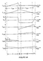
- Diode 24 is reverse biased during this time and energy is not transferred from input to output. This period is the first phase of operation shown as time period I in Fig. 4A.
- transistor 12 is turned off.
- the stored magnetic energy in inductor 15 maintains the flow of current in the same direction, charging capacitance 13 which shunts transistor 12. A portion of the current also flows through capacitor 20 and discharges capacitance 22 which shunts transistor 21.
- diode 24 becomes forward biased, and consequently a further portion of the current of inductor 15 begins to flow to the output through diode 24. Current does not flow through diode 25 since it is reverse biased.
- the remaining current in inductor 15 continues charging capacitance 13 and capacitance 22 until the voltage at node X equals the voltage across capacitor 20, at which time diode 23 begins to conduct.
- transistor 21 is approximately zero when diode 23 begins to conduct and charge does not accumulate across capacitance 22. The excess current in inductor 15 continues to transfer to charge capacitor 20. During this period (Period II), transistor 21 is turned on by the control circuit. Thus, since the voltage across transistor 21 is approximately zero when turned on, minimal switching loss occurs. This completes the second phase of operation shown as period II in Fig. 4A.
- inductor 15 and inductor 26 combine at node X, discharging capacitor 13 and charging capacitor 22 until the voltage at node X equals zero.
- the current in inductor 26 is then shunted through diode 25 since diode 24 is reverse biased.
- the remaining current in inductor 15 continues to discharge capacitor 13 until diode 14 conducts. At this time, any remaining energy in inductor 15 is returned to the input.
- the voltage across transistor 12 is approximately zero since charge does not accumulate across capacitance 13. This completes phase four, shown as period IV in Fig. 5.
- the control circuit again turns on transistor 12 to begin phase one of operation. It should be noted that since only a small voltage is impressed across transistor 12 when it is turned on, minimal switching loss occurs.
- the two switch, DC/DC converter 10 thus provides sufficient inductive energy storage at the termination of the "on" period of each switch to alter the charge on the intrinsic and stray capacitance of the combination of switches producing zero voltage across the alternate switch prior to its turn on.
- the short dead-band between the turn on pulses provided by the control circuit allows time for this transition.
- the energy stored in the capacitance of the switches is returned to the source and load rather than being dissipated in the switching devices. This greatly improves the efficiency of the converter, particularly when operating at high frequency.
- the topology of converter 10 provides other characteristics in addition to zero voltage switching such as operability at a constant frequency with pulse-width-modulation for regulation and quasi-square wave output current.
- a second embodiment of the invention is constructed by replacing inductor 15 with transformer 30.
- the circuit of Figure 5 is an isolated DC/DC converter in accordance with the invention.
- a gap in the magnetic path of transformer 30 sets the primary winding reactance equal to inductor 15 of Figure 4.
- transformer 30 has a dot at one terminal of the primary coil and a dot at one terminal of the secondary coil.
- a current entering the dotted terminal of one coil produces an open circuit voltage between the terminals of the second coil which is sensed in the direction indicated by a positive voltage reference at the dotted terminal of this second coil.
- the isolated converter is similar to that of the non-isolated converter described above.
- the waveform of Figure 5 illustrates the current flowing through the primary of transformer 30.
- intrinsic capacitance 34 shunting transistor 35 is discharged by energy stored in the primary of transformer 30 and in inductor 31 before the control turns on transistor 35. Hence, zero voltage switching is achieved and switching loss is minimized.
- the converter of Figure 5 has other advantages. Dielectric isolation between input and output is achieved.
- the output voltage may be changed with respect to the input voltage in accordance with the transformer turns ratio N S /N P .
- the input current may also be changed with respect to the output current in accordance with the turns ratio.
- incorporation of the transformer leakage reactance into the inductance of the primary of transformer 30 and into inductor 31 avoids the typical energy loss due to leakage reactance.
- Incorporation of the transformer winding capacitance into the intrinsic and distributed capacitance at node X avoids loss due to winding capacitance since energy charging the capacitance positively transfers to charge the capacitance negatively rather than dissipating.
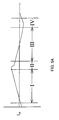
- Figure 5A shows a waveform of the primary winding current for an ideal transformer.
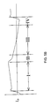
- Figure 5B shows the effect of leakage inductance on the waveform when a non-ideal transformer is used.
- the leakage inductance beneficially alters the peak to average current ratio, thereby reducing stress on components.
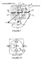
- a third embodiment of the invention is constructed by combining transformer 30 and inductor 31 of Figure 5 on a common magnetic core 40 as shown in Figure 6.
- the polarity of voltages, currents, and windings is such that the DC components of magnetic flux from the transformer leg and the inductor leg add to the third leg of the core, while the AC components of magnetic flux from the transformer leg and inductor leg subtract in the third leg.
- several other advantages of this embodiment are achieved. Due to the sharing of core material, the volume of the core is reduced and therefore the total core losses are proportionally reduced. In addition, since losses in magnetic cores are due only to the AC flux, the subtraction of flux in the third leg further reduces the loss in this portion of the core. Finally, the multiplicity of components is reduced.
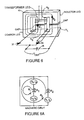
- a fourth embodiment of the invention is constructed by inserting a magnetic reluctance (gap) 50 in the third leg of composite core 40, as shown in the integrated transformer of Figure 7.
- the effect is such that during the conduction time of transistor 35 (interval I) energy is transferred from the primary of the transformer to the inductor leg, and the rate of decrease of current in the inductor and therefore diode 36 and the output circuits is abated and can be zero.
- transistor 32 during the conduction of transistor 32 (interval III), energy is transferred uniformly over the interval and the current in the inductor and therefore diode 37, the transformer secondary and the output circuits exhibits less change and can be constant.
- the benefits are decreased ripple current in the output, reduced stress on the output filter capacitor 38 and improved smoothing of the output voltage.
- N P I P + N S I S ⁇ 1R1 + ( ⁇ 1+ ⁇ 2)R3 (1)
- N L I L ⁇ 1R2 + ( ⁇ 1+ ⁇ 2)R3 (2)
- dI L /dt 0;
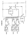
- a multiple output line embodiment of the invention as shown in Fig. 8 includes a transformer 80 having a plurality of secondary windings S-1 through S-N. During operation, output voltages V out1 through V outN are provided at output lines of the converter. Operation of the circuit is similar to the circuit of Fig. 5, and similar components are numbered identically.
- the plurality of inductors 31-1 through 31-N may be combined on a common core.
- transformer 80 and the plurality of inductors 31-1 through 31-N may be integrated together on a common core.
- the common core may have three legs each containing a magnetic gap.
- Discrete capacitive elements may be connected in parallel across each of the switching transistors (i.e. transistor 33 and 34) in order to reduce the rate of change of voltage across the switching devices.
- discrete inductance may be connected in series with the primary or secondary windings of the transformer incorporated within each of the isolated embodiments of the invention.
Landscapes
- Engineering & Computer Science (AREA)
- Power Engineering (AREA)
- Dc-Dc Converters (AREA)
- Amplifiers (AREA)
- Input Circuits Of Receivers And Coupling Of Receivers And Audio Equipment (AREA)
- Details Of Television Scanning (AREA)
Applications Claiming Priority (4)
| Application Number | Priority Date | Filing Date | Title |
|---|---|---|---|
| US07/436,394 US4959764A (en) | 1989-11-14 | 1989-11-14 | DC/DC converter switching at zero voltage |
| US436394 | 1989-11-14 | ||
| US07/542,478 US5066900A (en) | 1989-11-14 | 1990-06-22 | Dc/dc converter switching at zero voltage |
| US542478 | 1990-06-22 |
Publications (3)
| Publication Number | Publication Date |
|---|---|
| EP0428377A2 true EP0428377A2 (fr) | 1991-05-22 |
| EP0428377A3 EP0428377A3 (en) | 1991-07-17 |
| EP0428377B1 EP0428377B1 (fr) | 1996-01-03 |
Family
ID=27030942
Family Applications (1)
| Application Number | Title | Priority Date | Filing Date |
|---|---|---|---|
| EP90312367A Expired - Lifetime EP0428377B1 (fr) | 1989-11-14 | 1990-11-13 | Convertisseur continu-continu à circuit de commutation |
Country Status (11)
| Country | Link |
|---|---|
| US (1) | US5066900A (fr) |
| EP (1) | EP0428377B1 (fr) |
| JP (2) | JP2875879B2 (fr) |
| KR (1) | KR100186776B1 (fr) |
| AT (1) | ATE132671T1 (fr) |
| AU (1) | AU636400B2 (fr) |
| CA (1) | CA2028453A1 (fr) |
| DE (2) | DE428377T1 (fr) |
| ES (1) | ES2024394A4 (fr) |
| IE (1) | IE71049B1 (fr) |
| NO (1) | NO904926L (fr) |
Cited By (18)
| Publication number | Priority date | Publication date | Assignee | Title |
|---|---|---|---|---|
| GB2258351A (en) * | 1991-07-26 | 1993-02-03 | Motorola Inc | Dc-dc converter |
| EP0549920A1 (fr) * | 1991-12-31 | 1993-07-07 | Alcatel Standard Electrica, S.A. | Système de redresseur pour convertisseurs commutés par tension apériodique |
| EP0571067A1 (fr) * | 1992-04-21 | 1993-11-24 | Wisconsin Alumni Research Foundation | Convertisseur du type "forward" avec deux commutateurs actifs et aptitude à facteur de puissance unité |
| EP0617501A1 (fr) * | 1993-03-23 | 1994-09-28 | Linear Technology Corporation | Circuit de commande et méthode pour maintenir une grande efficacité couvrant un large domaine de courants dans un régulateur à découpage |
| EP0622891A3 (fr) * | 1993-04-29 | 1995-01-11 | At & T Corp | Redresseur synchrone à faibles pertes pour application à convertisseurs de puissance à tension limitée. |
| US5949226A (en) * | 1995-04-10 | 1999-09-07 | Kabushiki Kaisha Toyoda Jidoshokki Seisakush | DC/DC converter with reduced power consumpton and improved efficiency |
| US5998979A (en) * | 1997-10-28 | 1999-12-07 | Telefonaktiebolaget Lm Ericsson | Regulator |
| US6127815A (en) * | 1999-03-01 | 2000-10-03 | Linear Technology Corp. | Circuit and method for reducing quiescent current in a switching regulator |
| US6307356B1 (en) | 1998-06-18 | 2001-10-23 | Linear Technology Corporation | Voltage mode feedback burst mode circuit |
| USRE37510E1 (en) | 1995-05-25 | 2002-01-15 | Lucent Technologies Inc. | Self-synchronized drive circuit for a synchronized rectifier in a clamped-mode power converter |
| US6476589B2 (en) | 2001-04-06 | 2002-11-05 | Linear Technology Corporation | Circuits and methods for synchronizing non-constant frequency switching regulators with a phase locked loop |
| EP1120892A3 (fr) * | 2000-01-11 | 2003-10-22 | Murata Manufacturing Co., Ltd. | Unité d'alimentation de puissance à découpage |
| US6995483B2 (en) * | 2002-10-15 | 2006-02-07 | Texas Instruments Incorporated | Synchronous buck and boost regulator power reduction circuit using high side sensing |
| US7019507B1 (en) | 2003-11-26 | 2006-03-28 | Linear Technology Corporation | Methods and circuits for programmable current limit protection |
| US7030596B1 (en) | 2003-12-03 | 2006-04-18 | Linear Technology Corporation | Methods and circuits for programmable automatic burst mode control using average output current |
| TWI408881B (zh) * | 2011-04-18 | 2013-09-11 | Richtek Technology Corp | 多相電源轉換器的增強型相數控制電路及方法 |
| US9331578B2 (en) | 2013-07-12 | 2016-05-03 | Asustek Computer Inc. | Multi-phase buck DC converter |
| US10610627B2 (en) | 2014-05-29 | 2020-04-07 | St. Vincent's Hospital Sydney Limited | Ventricular assist device method and apparatus |
Families Citing this family (91)
| Publication number | Priority date | Publication date | Assignee | Title |
|---|---|---|---|---|
| JP2961897B2 (ja) * | 1990-12-10 | 1999-10-12 | 日本電気株式会社 | スイッチング電源装置 |
| US5399825A (en) * | 1991-03-01 | 1995-03-21 | Creare, Inc. | Inductor-charged electric discharge machining power supply |
| JP3151932B2 (ja) * | 1992-04-27 | 2001-04-03 | ヤマハ株式会社 | 電源回路 |
| US5355077A (en) * | 1992-04-27 | 1994-10-11 | Dell U.S.A., L.P. | High efficiency regulator with shoot-through current limiting |
| US5430640A (en) * | 1992-04-30 | 1995-07-04 | Samsung Electro-Mechanics Co., Ltd. | Power supply |
| US5262930A (en) * | 1992-06-12 | 1993-11-16 | The Center For Innovative Technology | Zero-voltage transition PWM converters |
| US5418704A (en) * | 1992-06-12 | 1995-05-23 | Center For Innovative Technology | Zero-voltage-transition pulse-width-modulated converters |
| US5341278A (en) * | 1992-08-20 | 1994-08-23 | Brooks Steven W | Switching pulsed resonant DC-DC converter power amplifier |
| US5343140A (en) * | 1992-12-02 | 1994-08-30 | Motorola, Inc. | Zero-voltage-switching quasi-resonant converters with multi-resonant bipolar switch |
| US5363289A (en) * | 1992-12-15 | 1994-11-08 | At&T Bell Laboratories | Control apparatus for limiting voltage on a core reset capacitor |
| US5282123A (en) * | 1992-12-16 | 1994-01-25 | At&T Bell Laboratories | Clamped mode DC-DC converter |
| US5307005A (en) * | 1992-12-23 | 1994-04-26 | International Business Machines Corporation | Zero current switching reverse recovery circuit |
| US5625541A (en) * | 1993-04-29 | 1997-04-29 | Lucent Technologies Inc. | Low loss synchronous rectifier for application to clamped-mode power converters |
| US5457620A (en) * | 1993-07-30 | 1995-10-10 | At&T Ipm Corp. | Current estimating circuit for switch mode power supply |
| US5485362A (en) * | 1993-09-08 | 1996-01-16 | Eos Corporation | Resonant power converter for changing the magnitude of a DC voltage |
| US5479337A (en) * | 1993-11-30 | 1995-12-26 | Kaiser Aerospace And Electronics Corporation | Very low power loss amplifier for analog signals utilizing constant-frequency zero-voltage-switching multi-resonant converter |
| US5446366A (en) * | 1994-02-08 | 1995-08-29 | Computer Products, Inc. | Boost converter power supply with reduced losses, control circuit and method therefor |
| US5444356A (en) * | 1994-03-03 | 1995-08-22 | Miller Electric Mfg. Co. | Buck converter having a variable output and method for buck converting power with a variable output |
| JPH0934564A (ja) * | 1995-07-18 | 1997-02-07 | Chiyoda:Kk | 入力波形追従型交流電源装置 |
| JP2792536B2 (ja) * | 1995-09-26 | 1998-09-03 | 日本電気株式会社 | 共振型dc−dcコンバータ |
| MY114795A (en) * | 1995-10-02 | 2003-01-31 | Thomson Consumer Electronics | Tuned switch-mode power supply with current mode control |
| US5600546A (en) * | 1995-10-16 | 1997-02-04 | Computer Products, Inc. | Input harmonic current corrected AC-to-DC converter with multiple coupled primary windings |
| US5652700A (en) * | 1995-10-16 | 1997-07-29 | Computer Products, Inc. | Low cost AC-to-DC converter having input current with reduced harmonics |
| JPH09215319A (ja) * | 1996-02-01 | 1997-08-15 | Toyota Autom Loom Works Ltd | Dc/dcコンバータ |
| US6225792B1 (en) | 1996-12-23 | 2001-05-01 | Phonak Ag | Method and apparatus for the supply of energy to a hearing device |
| US5959493A (en) * | 1996-05-06 | 1999-09-28 | Cassista; Philip A. | Totem pole driver circuit |
| US5973939A (en) * | 1996-08-29 | 1999-10-26 | Trw Inc. | Double forward converter with soft-PWM switching |
| TW349287B (en) * | 1996-09-12 | 1999-01-01 | Thomson Consumer Electronics | A forward converter with an inductor coupled to a transformer winding |
| EP1473968B1 (fr) * | 1996-12-04 | 2009-07-01 | Phonak Ag | Procédé et dispositif d'alimentation d'une prothèse auditive |
| US5808879A (en) * | 1996-12-26 | 1998-09-15 | Philips Electronics North America Corporatin | Half-bridge zero-voltage-switched PWM flyback DC/DC converter |
| JP2002514378A (ja) | 1997-01-24 | 2002-05-14 | シンクォール・インコーポレーテッド | 高効率電力変換装置 |
| US7269034B2 (en) | 1997-01-24 | 2007-09-11 | Synqor, Inc. | High efficiency power converter |
| US5774346A (en) * | 1997-01-24 | 1998-06-30 | Poon; Franki Ngai Kit | Family of zero voltage switching DC to DC converters with coupled output inductor |
| US6018469A (en) * | 1997-02-05 | 2000-01-25 | Computer Products, Inc. | Low cost high efficiency power converter |
| US5880940A (en) * | 1997-02-05 | 1999-03-09 | Computer Products, Inc. | Low cost high efficiency power converter |
| US5912552A (en) * | 1997-02-12 | 1999-06-15 | Kabushiki Kaisha Toyoda Jidoshokki Seisakusho | DC to DC converter with high efficiency for light loads |
| JPH10313572A (ja) * | 1997-05-09 | 1998-11-24 | Toyota Autom Loom Works Ltd | スイッチングレギュレータ制御方式 |
| US6038146A (en) * | 1997-06-13 | 2000-03-14 | Computer Products, Incorporated | High power factors, single stage harmonics correction converter |
| KR100455651B1 (ko) * | 1997-08-08 | 2005-01-17 | 삼성전자주식회사 | 다중출력 직류/직류 전압 변환장치 및 이를 이용한 액정 표시 장치 |
| US6023154A (en) * | 1997-10-28 | 2000-02-08 | International Rectifier Corporation | Parallel and interwoven buck converter for high efficiency, low voltage power supply |
| US5920473A (en) * | 1998-03-09 | 1999-07-06 | Magnetic Technology, Inc. | Dc-to-Dc power converter with integrated magnetic power transformer |
| US6614288B1 (en) * | 1998-05-20 | 2003-09-02 | Astec International Limited | Adaptive drive circuit for zero-voltage and low-voltage switches |
| US6081432A (en) | 1998-05-26 | 2000-06-27 | Artesyn Technologies, Inc. | Active reset forward converter employing synchronous rectifiers |
| US6259235B1 (en) * | 1999-08-26 | 2001-07-10 | Tyco Electronics Logistics Ag | Active clamp for power converter and method of operation thereof |
| US6370051B1 (en) | 1999-11-05 | 2002-04-09 | Power-One, Inc. | Forward converter circuit having reduced switching losses |
| JP3317950B2 (ja) * | 2000-01-24 | 2002-08-26 | 甲府日本電気株式会社 | アクティブクランプフォアワードコンバータ |
| US6400579B2 (en) * | 2000-03-24 | 2002-06-04 | Slobodan Cuk | Lossless switching DC to DC converter with DC transformer |
| US6198260B1 (en) * | 2000-06-05 | 2001-03-06 | Technical Witts, Inc. | Zero voltage switching active reset power converters |
| US6252383B1 (en) * | 2000-07-11 | 2001-06-26 | Technical Witts, Inc. | Buck and boost power converters with non-pulsating input and output terminal currents |
| KR100361840B1 (ko) * | 2000-07-25 | 2002-11-23 | 삼성전기주식회사 | 영전압 스위칭 컨버터 회로 |
| US6462962B1 (en) | 2000-09-08 | 2002-10-08 | Slobodan Cuk | Lossless switching DC-to-DC converter |
| JP2004512798A (ja) * | 2000-10-27 | 2004-04-22 | コーニンクレッカ フィリップス エレクトロニクス エヌ ヴィ | コンバータ制御 |
| US6674274B2 (en) | 2001-02-08 | 2004-01-06 | Linear Technology Corporation | Multiple phase switching regulators with stage shedding |
| US6466460B1 (en) | 2001-08-24 | 2002-10-15 | Northrop Grumman Corporation | High efficiency, low voltage to high voltage power converter |
| AU2003238828A1 (en) * | 2002-05-24 | 2003-12-12 | Arizona Board Of Regents | Integrated zvs synchronous buck dc-dc converter with adaptive control |
| US6939347B2 (en) | 2002-11-19 | 2005-09-06 | Conmed Corporation | Electrosurgical generator and method with voltage and frequency regulated high-voltage current mode power supply |
| US7002323B2 (en) * | 2003-05-07 | 2006-02-21 | Nec Corporation | Switching power supply circuit capable of reducing switching loss and control method used therein |
| US9956639B2 (en) | 2005-02-07 | 2018-05-01 | Lincoln Global, Inc | Modular power source for electric ARC welding and output chopper |
| US8785816B2 (en) | 2004-07-13 | 2014-07-22 | Lincoln Global, Inc. | Three stage power source for electric arc welding |
| US8269141B2 (en) | 2004-07-13 | 2012-09-18 | Lincoln Global, Inc. | Power source for electric arc welding |
| US8581147B2 (en) | 2005-03-24 | 2013-11-12 | Lincoln Global, Inc. | Three stage power source for electric ARC welding |
| US7133298B2 (en) * | 2004-10-25 | 2006-11-07 | Texas Instruments Incorporated | High frequency voltage regulating transformer based converter |
| DE102004061341A1 (de) * | 2004-12-20 | 2006-07-06 | Puls Gmbh | Stromversorgung |
| US9855620B2 (en) | 2005-02-07 | 2018-01-02 | Lincoln Global, Inc. | Welding system and method of welding |
| US9647555B2 (en) | 2005-04-08 | 2017-05-09 | Lincoln Global, Inc. | Chopper output stage for arc welder power source |
| US20070013349A1 (en) * | 2005-07-18 | 2007-01-18 | Bassett John A | Zero voltage switching buck converter |
| JP4861040B2 (ja) * | 2006-04-06 | 2012-01-25 | 株式会社日立製作所 | 単方向dc−dcコンバータ |
| US7786712B2 (en) * | 2006-12-30 | 2010-08-31 | Advanced Analogic Technologies, Inc. | High-efficiency DC/DC voltage converter including up inductive switching pre-regulator and capacitive switching post-converter |
| US7777459B2 (en) * | 2006-12-30 | 2010-08-17 | Advanced Analogic Technologies, Inc. | High-efficiency DC/DC voltage converter including capacitive switching pre-converter and down inductive switching post-regulator |
| BRPI0721576A2 (pt) | 2007-05-25 | 2013-01-15 | Thomson Licensing | suprimento de energia elÉtrica |
| US8040704B2 (en) * | 2007-06-30 | 2011-10-18 | Cuks, Llc | Integrated magnetics switching converter with zero inductor and output ripple currents and lossless switching |
| EP2188889A1 (fr) * | 2007-09-01 | 2010-05-26 | Brusa Elektronik AG | Convertisseur de puissance de commutation à tension nulle |
| KR100983033B1 (ko) * | 2008-03-17 | 2010-09-17 | 삼성전기주식회사 | 집적화된 트랜스포머 및 이를 이용한 전원 장치 |
| JP4643695B2 (ja) | 2008-09-02 | 2011-03-02 | 日立コンピュータ機器株式会社 | 双方向dc−dcコンバータ及びその制御方法 |
| EP2385617A1 (fr) * | 2010-05-06 | 2011-11-09 | Brusa Elektronik AG | Commande et procédé pour un convertisseur de courant continu et convertisseur de courant continu |
| JP5319630B2 (ja) * | 2010-09-03 | 2013-10-16 | 本田技研工業株式会社 | 複合型変圧器 |
| TW201218598A (en) * | 2010-10-29 | 2012-05-01 | xiang-yu Li | which combines a power supply and a voltage boost/buck circuit to regulate an output voltage of the power supply into a target voltage |
| US9385607B2 (en) | 2010-10-29 | 2016-07-05 | Superc-Touch Corporation | Safe electric power regulating circuit |
| US10103632B2 (en) | 2011-04-18 | 2018-10-16 | Richtek Technology Corp. | Enhanced phase control circuit and method for a multiphase power converter |
| CN102223075B (zh) * | 2011-06-16 | 2013-07-24 | 清华大学 | 一种四端口直流变换器 |
| US8520413B2 (en) * | 2011-08-17 | 2013-08-27 | Mks Instruments, Inc. | Adjustable resonant buck converter |
| JP6103874B2 (ja) * | 2012-10-12 | 2017-03-29 | 株式会社日立情報通信エンジニアリング | 電源装置とその運転方法 |
| NZ724432A (en) * | 2012-11-23 | 2018-02-23 | Elevare Energy Ip Pty Ltd | Electrical supply system |
| US10199950B1 (en) | 2013-07-02 | 2019-02-05 | Vlt, Inc. | Power distribution architecture with series-connected bus converter |
| US9465074B2 (en) * | 2013-10-09 | 2016-10-11 | Ford Global Technologies, Llc | System and method for measuring switching loss associated with semiconductor switching devices |
| US10186949B1 (en) * | 2017-11-09 | 2019-01-22 | International Business Machines Corporation | Coupled-inductor DC-DC power converter |
| EP3764529B1 (fr) * | 2018-03-07 | 2022-09-21 | Nissan Motor Co., Ltd. | Dispositif de conversion de courant résonnant et son procédé de commande, et convertisseur cc-cc |
| CA3153706A1 (fr) | 2019-09-09 | 2021-03-18 | Elexsys Ip Pty Ltd | Reseau de distribution d'energie electrique bidirectionnel |
| CA3153704A1 (fr) | 2019-09-09 | 2021-03-18 | Elexsys Ip Pty Ltd | Appareil de regulation de puissance electrique |
| US12626851B2 (en) | 2021-07-04 | 2026-05-12 | The Research Foundation For The State University Of New York | High frequency integrated planar magnetics for a bidirectional AC to DC CLLC resonant converter |
| TWI879198B (zh) * | 2023-11-01 | 2025-04-01 | 國立臺灣科技大學 | 具有箝位機制的電源轉換器 |
Family Cites Families (12)
| Publication number | Priority date | Publication date | Assignee | Title |
|---|---|---|---|---|
| US444146A (en) * | 1891-01-06 | Automatic pneumatic brake | ||
| US4415959A (en) * | 1981-03-20 | 1983-11-15 | Vicor Corporation | Forward converter switching at zero current |
| US4441146A (en) * | 1982-02-04 | 1984-04-03 | Vicor Corporation | Optimal resetting of the transformer's core in single ended forward converters |
| JPS6162360A (ja) * | 1984-09-03 | 1986-03-31 | Hitachi Ltd | 多出力スイツチング電源回路 |
| US4669036A (en) * | 1986-06-13 | 1987-05-26 | Allied Corporation | d.c. to d.c. converter power supply with dual regulated outputs |
| US4720668A (en) * | 1986-06-20 | 1988-01-19 | Lee Fred C | Zero-voltage switching quasi-resonant converters |
| US4672303A (en) * | 1986-08-28 | 1987-06-09 | International Business Machines Corporation | Inductor current control circuit |
| US4727308A (en) * | 1986-08-28 | 1988-02-23 | International Business Machines Corporation | FET power converter with reduced switching loss |
| US4734839A (en) * | 1987-03-23 | 1988-03-29 | Barthold Fred O | Source volt-ampere/load volt-ampere differential converter |
| US4867822A (en) * | 1987-08-04 | 1989-09-19 | The Boeing Corporation | Method for in-place fabrication of graphite epoxy bushings in graphite epoxy structures |
| US4857822A (en) * | 1987-09-23 | 1989-08-15 | Virginia Tech Intellectual Properties, Inc. | Zero-voltage-switched multi-resonant converters including the buck and forward type |
| US4935858A (en) * | 1989-09-05 | 1990-06-19 | Motorola, Inc. | Auxiliary output regulation technique for power supplies |
-
1990
- 1990-06-22 US US07/542,478 patent/US5066900A/en not_active Expired - Lifetime
- 1990-10-16 IE IE370790A patent/IE71049B1/en not_active IP Right Cessation
- 1990-10-18 AU AU64703/90A patent/AU636400B2/en not_active Ceased
- 1990-10-24 CA CA002028453A patent/CA2028453A1/fr not_active Abandoned
- 1990-11-12 KR KR1019900018231A patent/KR100186776B1/ko not_active Expired - Fee Related
- 1990-11-13 AT AT90312367T patent/ATE132671T1/de active
- 1990-11-13 DE DE199090312367T patent/DE428377T1/de active Pending
- 1990-11-13 ES ES90312367T patent/ES2024394A4/es active Pending
- 1990-11-13 EP EP90312367A patent/EP0428377B1/fr not_active Expired - Lifetime
- 1990-11-13 DE DE69024614T patent/DE69024614T2/de not_active Expired - Fee Related
- 1990-11-13 NO NO90904926A patent/NO904926L/no unknown
- 1990-11-14 JP JP2308431A patent/JP2875879B2/ja not_active Expired - Fee Related
-
1998
- 1998-05-26 JP JP10143720A patent/JPH10327577A/ja active Pending
Cited By (30)
| Publication number | Priority date | Publication date | Assignee | Title |
|---|---|---|---|---|
| GB2258351B (en) * | 1991-07-26 | 1995-04-26 | Motorola Inc | Voltage conversion circuit |
| GB2258351A (en) * | 1991-07-26 | 1993-02-03 | Motorola Inc | Dc-dc converter |
| EP0549920A1 (fr) * | 1991-12-31 | 1993-07-07 | Alcatel Standard Electrica, S.A. | Système de redresseur pour convertisseurs commutés par tension apériodique |
| EP0571067A1 (fr) * | 1992-04-21 | 1993-11-24 | Wisconsin Alumni Research Foundation | Convertisseur du type "forward" avec deux commutateurs actifs et aptitude à facteur de puissance unité |
| US5481178A (en) * | 1993-03-23 | 1996-01-02 | Linear Technology Corporation | Control circuit and method for maintaining high efficiency over broad current ranges in a switching regulator circuit |
| US5731694A (en) * | 1993-03-23 | 1998-03-24 | Linear Technology Corporation | Control circuit and method for maintaining high efficiency over broard current ranges in a switching regulator circuit |
| US6580258B2 (en) | 1993-03-23 | 2003-06-17 | Linear Technology Corporation | Control circuit and method for maintaining high efficiency over broad current ranges in a switching regulator circuit |
| US5994885A (en) * | 1993-03-23 | 1999-11-30 | Linear Technology Corporation | Control circuit and method for maintaining high efficiency over broad current ranges in a switching regulator circuit |
| US6304066B1 (en) | 1993-03-23 | 2001-10-16 | Linear Technology Corporation | Control circuit and method for maintaining high efficiency over broad current ranges in a switching regular circuit |
| EP0617501A1 (fr) * | 1993-03-23 | 1994-09-28 | Linear Technology Corporation | Circuit de commande et méthode pour maintenir une grande efficacité couvrant un large domaine de courants dans un régulateur à découpage |
| EP0622891A3 (fr) * | 1993-04-29 | 1995-01-11 | At & T Corp | Redresseur synchrone à faibles pertes pour application à convertisseurs de puissance à tension limitée. |
| EP1052763A1 (fr) * | 1993-04-29 | 2000-11-15 | AT&T Corp. | Redresseur synchron à pertes reduites pour l'application dans des convertisseurs prépolarisé |
| USRE36571E (en) * | 1993-04-29 | 2000-02-15 | Lucent Technologies Inc. | Low loss synchronous rectifier for application to clamped-mode power converters |
| US6157182A (en) * | 1995-04-10 | 2000-12-05 | Kabushiki Kaisha Toyoda | DC/DC converter with multiple operating modes |
| US5949226A (en) * | 1995-04-10 | 1999-09-07 | Kabushiki Kaisha Toyoda Jidoshokki Seisakush | DC/DC converter with reduced power consumpton and improved efficiency |
| USRE37510E1 (en) | 1995-05-25 | 2002-01-15 | Lucent Technologies Inc. | Self-synchronized drive circuit for a synchronized rectifier in a clamped-mode power converter |
| US5998979A (en) * | 1997-10-28 | 1999-12-07 | Telefonaktiebolaget Lm Ericsson | Regulator |
| US6307356B1 (en) | 1998-06-18 | 2001-10-23 | Linear Technology Corporation | Voltage mode feedback burst mode circuit |
| US6366066B1 (en) | 1999-03-01 | 2002-04-02 | Milton E. Wilcox | Circuit and method for reducing quiescent current in a switching regulator |
| US6127815A (en) * | 1999-03-01 | 2000-10-03 | Linear Technology Corp. | Circuit and method for reducing quiescent current in a switching regulator |
| EP1120892A3 (fr) * | 2000-01-11 | 2003-10-22 | Murata Manufacturing Co., Ltd. | Unité d'alimentation de puissance à découpage |
| US6774611B2 (en) | 2001-04-06 | 2004-08-10 | Linear Technology Corporation | Circuits and methods for synchronizing non-constant frequency switching regulators with a phase locked loop |
| US6476589B2 (en) | 2001-04-06 | 2002-11-05 | Linear Technology Corporation | Circuits and methods for synchronizing non-constant frequency switching regulators with a phase locked loop |
| US7019497B2 (en) | 2001-04-06 | 2006-03-28 | Linear Technology Corporation | Circuits and methods for synchronizing non-constant frequency switching regulators with a phase locked loop |
| US6995483B2 (en) * | 2002-10-15 | 2006-02-07 | Texas Instruments Incorporated | Synchronous buck and boost regulator power reduction circuit using high side sensing |
| US7019507B1 (en) | 2003-11-26 | 2006-03-28 | Linear Technology Corporation | Methods and circuits for programmable current limit protection |
| US7030596B1 (en) | 2003-12-03 | 2006-04-18 | Linear Technology Corporation | Methods and circuits for programmable automatic burst mode control using average output current |
| TWI408881B (zh) * | 2011-04-18 | 2013-09-11 | Richtek Technology Corp | 多相電源轉換器的增強型相數控制電路及方法 |
| US9331578B2 (en) | 2013-07-12 | 2016-05-03 | Asustek Computer Inc. | Multi-phase buck DC converter |
| US10610627B2 (en) | 2014-05-29 | 2020-04-07 | St. Vincent's Hospital Sydney Limited | Ventricular assist device method and apparatus |
Also Published As
| Publication number | Publication date |
|---|---|
| EP0428377B1 (fr) | 1996-01-03 |
| DE69024614D1 (de) | 1996-02-15 |
| JPH10327577A (ja) | 1998-12-08 |
| KR910010809A (ko) | 1991-06-29 |
| DE69024614T2 (de) | 1996-06-27 |
| ES2024394A4 (es) | 1992-03-01 |
| AU636400B2 (en) | 1993-04-29 |
| AU6470390A (en) | 1991-05-23 |
| JP2875879B2 (ja) | 1999-03-31 |
| NO904926D0 (no) | 1990-11-13 |
| IE903707A1 (en) | 1991-05-22 |
| JPH03173349A (ja) | 1991-07-26 |
| ATE132671T1 (de) | 1996-01-15 |
| KR100186776B1 (ko) | 1999-05-15 |
| IE71049B1 (en) | 1997-01-15 |
| EP0428377A3 (en) | 1991-07-17 |
| NO904926L (no) | 1991-05-15 |
| DE428377T1 (de) | 1991-12-19 |
| US5066900A (en) | 1991-11-19 |
| CA2028453A1 (fr) | 1991-05-15 |
Similar Documents
| Publication | Publication Date | Title |
|---|---|---|
| EP0428377B1 (fr) | Convertisseur continu-continu à circuit de commutation | |
| US4959764A (en) | DC/DC converter switching at zero voltage | |
| EP0759654B1 (fr) | Convertisseur à découpage avec courant d'entrée et courant de sortie continus | |
| US5132888A (en) | Interleaved bridge converter | |
| US5886882A (en) | Push-pull DC-DC converter with transformer having multiple primary and secondary windings with diodes connected between them with MOSFET switching | |
| CA1121453A (fr) | Commutateur-convertisseur de c.c. a c.c. | |
| EP0508664B1 (fr) | Convertisseur continu-continu | |
| US6272023B1 (en) | High efficiency coupled inductor soft switching power converters | |
| US6147886A (en) | Dual opposed interleaved coupled inductor soft switching converters | |
| US5796595A (en) | Interleaved continuous flyback power converter system | |
| US5122728A (en) | Coupled inductor type dc to dc converter with single magnetic component | |
| US6304065B1 (en) | Power electronic circuits with all terminal currents non-pulsating | |
| US7471524B1 (en) | Isolated DC-DC converters with high current capability | |
| US7239530B1 (en) | Apparatus for isolated switching power supply with coupled output inductors | |
| US6411153B2 (en) | Universal pulse width modulated zero voltage transition switching cell | |
| US5436818A (en) | Full wave buck-boost power converter with buck power converter properties | |
| US6452814B1 (en) | Zero voltage switching cells for power converters | |
| Zhou et al. | A Novel High-input-voltage, High Efficiency and Fast Transient Voltage Regulator Module | |
| US6590791B1 (en) | High input voltage, high efficiency, fast transient voltage regulator module (VRM) | |
| WO2005022732A2 (fr) | Convertisseurs de puissance a pont integral a commutation sans tension | |
| GB2417145A (en) | DC to DC converter with high frequency zig-zag transformer | |
| US5870291A (en) | Asymmetrical half-bridge converter having adjustable parasitic resistances to offset output voltage DC bias | |
| US20030123264A1 (en) | Half-bridge isolation stage topologies | |
| US6166927A (en) | Push-pull power converter circuit | |
| EP0720278B1 (fr) | Régulateur à limitation de puissance |
Legal Events
| Date | Code | Title | Description |
|---|---|---|---|
| PUAI | Public reference made under article 153(3) epc to a published international application that has entered the european phase |
Free format text: ORIGINAL CODE: 0009012 |
|
| AK | Designated contracting states |
Kind code of ref document: A2 Designated state(s): AT BE CH DE DK ES FR GB GR IT LI LU NL SE |
|
| PUAL | Search report despatched |
Free format text: ORIGINAL CODE: 0009013 |
|
| AK | Designated contracting states |
Kind code of ref document: A3 Designated state(s): AT BE CH DE DK ES FR GB GR IT LI LU NL SE |
|
| RHK1 | Main classification (correction) |
Ipc: H02M 3/158 |
|
| EL | Fr: translation of claims filed | ||
| 17P | Request for examination filed |
Effective date: 19910924 |
|
| DET | De: translation of patent claims | ||
| REG | Reference to a national code |
Ref country code: ES Ref legal event code: BA2A Ref document number: 2024394 Country of ref document: ES Kind code of ref document: A4 |
|
| 17Q | First examination report despatched |
Effective date: 19930719 |
|
| ITF | It: translation for a ep patent filed | ||
| GRAA | (expected) grant |
Free format text: ORIGINAL CODE: 0009210 |
|
| AK | Designated contracting states |
Kind code of ref document: B1 Designated state(s): AT BE CH DE DK ES FR GB GR IT LI LU NL SE |
|
| PG25 | Lapsed in a contracting state [announced via postgrant information from national office to epo] |
Ref country code: AT Effective date: 19960103 Ref country code: DK Effective date: 19960103 Ref country code: LI Effective date: 19960103 Ref country code: CH Effective date: 19960103 Ref country code: NL Free format text: LAPSE BECAUSE OF FAILURE TO SUBMIT A TRANSLATION OF THE DESCRIPTION OR TO PAY THE FEE WITHIN THE PRESCRIBED TIME-LIMIT Effective date: 19960103 Ref country code: GR Free format text: LAPSE BECAUSE OF FAILURE TO SUBMIT A TRANSLATION OF THE DESCRIPTION OR TO PAY THE FEE WITHIN THE PRESCRIBED TIME-LIMIT Effective date: 19960103 |
|
| REF | Corresponds to: |
Ref document number: 132671 Country of ref document: AT Date of ref document: 19960115 Kind code of ref document: T |
|
| REF | Corresponds to: |
Ref document number: 69024614 Country of ref document: DE Date of ref document: 19960215 |
|
| ET | Fr: translation filed | ||
| PG25 | Lapsed in a contracting state [announced via postgrant information from national office to epo] |
Ref country code: ES Free format text: LAPSE BECAUSE OF FAILURE TO SUBMIT A TRANSLATION OF THE DESCRIPTION OR TO PAY THE FEE WITHIN THE PRESCRIBED TIME-LIMIT Effective date: 19960414 |
|
| NLV1 | Nl: lapsed or annulled due to failure to fulfill the requirements of art. 29p and 29m of the patents act | ||
| REG | Reference to a national code |
Ref country code: CH Ref legal event code: PL |
|
| PLBE | No opposition filed within time limit |
Free format text: ORIGINAL CODE: 0009261 |
|
| STAA | Information on the status of an ep patent application or granted ep patent |
Free format text: STATUS: NO OPPOSITION FILED WITHIN TIME LIMIT |
|
| PG25 | Lapsed in a contracting state [announced via postgrant information from national office to epo] |
Ref country code: LU Free format text: LAPSE BECAUSE OF NON-PAYMENT OF DUE FEES Effective date: 19961130 |
|
| 26N | No opposition filed | ||
| REG | Reference to a national code |
Ref country code: GB Ref legal event code: IF02 |
|
| PGFP | Annual fee paid to national office [announced via postgrant information from national office to epo] |
Ref country code: SE Payment date: 20021018 Year of fee payment: 13 |
|
| PGFP | Annual fee paid to national office [announced via postgrant information from national office to epo] |
Ref country code: BE Payment date: 20021202 Year of fee payment: 13 |
|
| PG25 | Lapsed in a contracting state [announced via postgrant information from national office to epo] |
Ref country code: SE Free format text: LAPSE BECAUSE OF NON-PAYMENT OF DUE FEES Effective date: 20031116 |
|
| PG25 | Lapsed in a contracting state [announced via postgrant information from national office to epo] |
Ref country code: BE Free format text: LAPSE BECAUSE OF NON-PAYMENT OF DUE FEES Effective date: 20031130 |
|
| BERE | Be: lapsed |
Owner name: *COMPUTER PRODUCTS INC. Effective date: 20031130 |
|
| EUG | Se: european patent has lapsed | ||
| REG | Reference to a national code |
Ref country code: FR Ref legal event code: CD |
|
| PGFP | Annual fee paid to national office [announced via postgrant information from national office to epo] |
Ref country code: FR Payment date: 20061117 Year of fee payment: 17 |
|
| PGFP | Annual fee paid to national office [announced via postgrant information from national office to epo] |
Ref country code: GB Payment date: 20061122 Year of fee payment: 17 |
|
| PGFP | Annual fee paid to national office [announced via postgrant information from national office to epo] |
Ref country code: IT Payment date: 20061130 Year of fee payment: 17 |
|
| PGFP | Annual fee paid to national office [announced via postgrant information from national office to epo] |
Ref country code: DE Payment date: 20070102 Year of fee payment: 17 |
|
| GBPC | Gb: european patent ceased through non-payment of renewal fee |
Effective date: 20071113 |
|
| PG25 | Lapsed in a contracting state [announced via postgrant information from national office to epo] |
Ref country code: DE Free format text: LAPSE BECAUSE OF NON-PAYMENT OF DUE FEES Effective date: 20080603 |
|
| REG | Reference to a national code |
Ref country code: FR Ref legal event code: ST Effective date: 20080930 |
|
| PG25 | Lapsed in a contracting state [announced via postgrant information from national office to epo] |
Ref country code: GB Free format text: LAPSE BECAUSE OF NON-PAYMENT OF DUE FEES Effective date: 20071113 |
|
| PG25 | Lapsed in a contracting state [announced via postgrant information from national office to epo] |
Ref country code: FR Free format text: LAPSE BECAUSE OF NON-PAYMENT OF DUE FEES Effective date: 20071130 |
|
| PG25 | Lapsed in a contracting state [announced via postgrant information from national office to epo] |
Ref country code: IT Free format text: LAPSE BECAUSE OF NON-PAYMENT OF DUE FEES Effective date: 20071113 |