EP0429018B1 - Halbleiterspeicheranordnung mit Eingangs-/Ausgangs-Datensignalleitungen, die Bitinformation in Hochgeschwindigkeit übertragen unabhängig von der Schwankung des Speisespannungssignals - Google Patents
Halbleiterspeicheranordnung mit Eingangs-/Ausgangs-Datensignalleitungen, die Bitinformation in Hochgeschwindigkeit übertragen unabhängig von der Schwankung des Speisespannungssignals Download PDFInfo
- Publication number
- EP0429018B1 EP0429018B1 EP90121957A EP90121957A EP0429018B1 EP 0429018 B1 EP0429018 B1 EP 0429018B1 EP 90121957 A EP90121957 A EP 90121957A EP 90121957 A EP90121957 A EP 90121957A EP 0429018 B1 EP0429018 B1 EP 0429018B1
- Authority
- EP
- European Patent Office
- Prior art keywords
- data signal
- signal lines
- voltage level
- input
- lines
- Prior art date
- Legal status (The legal status is an assumption and is not a legal conclusion. Google has not performed a legal analysis and makes no representation as to the accuracy of the status listed.)
- Expired - Lifetime
Links
Images




Classifications
-
- G—PHYSICS
- G11—INFORMATION STORAGE
- G11C—STATIC STORES
- G11C11/00—Digital stores characterised by the use of particular electric or magnetic storage elements; Storage elements therefor
- G11C11/21—Digital stores characterised by the use of particular electric or magnetic storage elements; Storage elements therefor using electric elements
- G11C11/34—Digital stores characterised by the use of particular electric or magnetic storage elements; Storage elements therefor using electric elements using semiconductor devices
- G11C11/40—Digital stores characterised by the use of particular electric or magnetic storage elements; Storage elements therefor using electric elements using semiconductor devices using transistors
- G11C11/401—Digital stores characterised by the use of particular electric or magnetic storage elements; Storage elements therefor using electric elements using semiconductor devices using transistors forming cells needing refreshing or charge regeneration, i.e. dynamic cells
-
- G—PHYSICS
- G11—INFORMATION STORAGE
- G11C—STATIC STORES
- G11C7/00—Arrangements for writing information into, or reading information out from, a digital store
- G11C7/10—Input/output [I/O] data interface arrangements, e.g. I/O data control circuits, I/O data buffers
- G11C7/1048—Data bus control circuits, e.g. precharging, presetting, equalising
-
- G—PHYSICS
- G11—INFORMATION STORAGE
- G11C—STATIC STORES
- G11C11/00—Digital stores characterised by the use of particular electric or magnetic storage elements; Storage elements therefor
- G11C11/21—Digital stores characterised by the use of particular electric or magnetic storage elements; Storage elements therefor using electric elements
- G11C11/34—Digital stores characterised by the use of particular electric or magnetic storage elements; Storage elements therefor using electric elements using semiconductor devices
- G11C11/40—Digital stores characterised by the use of particular electric or magnetic storage elements; Storage elements therefor using electric elements using semiconductor devices using transistors
- G11C11/401—Digital stores characterised by the use of particular electric or magnetic storage elements; Storage elements therefor using electric elements using semiconductor devices using transistors forming cells needing refreshing or charge regeneration, i.e. dynamic cells
- G11C11/4063—Auxiliary circuits, e.g. for addressing, decoding, driving, writing, sensing or timing
- G11C11/407—Auxiliary circuits, e.g. for addressing, decoding, driving, writing, sensing or timing for memory cells of the field-effect type
- G11C11/409—Read-write [R-W] circuits
- G11C11/4096—Input/output [I/O] data management or control circuits, e.g. reading or writing circuits, I/O drivers or bit-line switches
Definitions
- This invention relates to a semiconductor memory device and, more particularly, to input/output data signal lines propagating a data bit at high speed regardless of fluctuation in power voltage level.
- FIG. 1 A typical example of the semiconductor memory device is illustrated in Fig. 1 of the drawings. A similar device is known from US-A-4 740 921. Another static RAM in which resistive means connected between data line pairs tend to equalize the data line potentials can be found in EP-A-0 037 625.
- a memory cell array 1 having a plurality of memory cells 1a and 1b coupled between a plurality of bit lines 2a and 2b and a voltage supply line VL, a combined circuit 3 of a precharging circuit and an equalization circuit provided for the bit lines 2a and 2b, a sense amplifier circuit 4 coupled to the bit lines 2a and 2b, a column selector circuit 5 coupled between the bit lines 2a and 2b and a pair of input/output data signal lines 6a and 6b, a combined circuit 7 of a precharging circuit and an equalization circuit provided for the input/output data signal lines 6a and 6b, a pull-up circuit 7 associated with the input/output data signal lines 6a and 6b, and a data amplifier circuit 8 coupled to the input/output data signal lines 6a and 6b.
- Each of the memory cells 1a and 1b is implemented by a series combination of a switching transistor Q1 and a storage capacitor C1 which is coupled between one of the bit lines 2a and 2b and a voltage line.
- a data bit is stored in each of the memory cells 1a and 1b in the form of electric charges, and the storage capacitor C1 accumulates the electric charges.
- a plurality of word lines W1 and W2 are provided in association with the memory cell array 1, and the switching transistors Q1 are selectively gated by the word lines W1 and W2 on the basis of row address bits.
- the sense amplifier circuit 4 is implemented by two series combinations of p-channel type field effect transistors Q2 and Q3 and n-channel type field effect transistors Q4 and Q5, and the two series combinations are coupled in parallel between two activation signal lines SAP and SANB. Though not shown in Fig. 1, a plurality of bit line pairs each associated with a sense amplifier circuit are respectively coupled to n-channel type filed effect transistors incorporated in the column selector circuit 5, and a control signal YSW allows a pair of n-channel type field effect transistors Q6 and Q7 to turn.
- the combined circuit 7 comprises a series combination of p-channel type field effect transistors Q8 and Q9 coupled between the input/output data signal lines 6a and 6b, and a p-channel type field effect transistor Q10 coupled in parallel to the series combination of the p-channel type field effect transistors Q8 and Q9, and the p-channel type field effect transistors Q8 to Q10 are concurrently gated by a precharging signal PIO so as to precharge and equalize the input/output data signal lines 6a and 6b at a precharging voltage level VCVT.
- the pull-up circuit 7 has two n-channel type field effect transistors Q11 and Q12 coupled between a source of positive voltage level Vcc and the input/output data signal lines 6a and 6b, respectively.
- the word line W1 is selected on the basis of the row address bits, and the word line W1 goes up at time t1, and the word line W1 exceeds the positive voltage level Vcc. Then, the switching transistor Q1 fully turns on, and the storage capacitor C1 is coupled through the switching transistor Q1 to the bit line 2a.
- the electric charges accumulated in the storage capacitor C1 are slightly discharged to the bit line 2a, and, for this reason, the storage capacitor C1 is decayed in voltage level at time t2 as shown in Fig. 2A. While the storage capacitor C1 is discharging the electric charges, the bit line 2a slightly goes up as shown in Fig. 2B, and a small difference takes place between the bit lines 2a and 2b.
- the sense amplifier circuit 4 When the activation signal lines SAP and SANB are driven toward the positive voltage level SAP and the ground voltage level SANB, respectively, then the sense amplifier circuit 4 is activated and increases the small difference in magnitude between the bit lines 2a and 2b together with the activation signals SAP and SANB. After the activation of the sense amplifier circuit 4, the precharging signal PIO goes up from the ground voltage level to the positive voltage level Vcc at time t3, and the input/output data signal lines 6a and 6b are blocked from the source of the precharging voltage level VCVT as shown in Fig. 2C.
- a read mode signal RM goes up to the positive high voltage level Vcc at time t4, and the n-channel type field effect transistors Q11 and Q12 turn on to couple the input/output data signal lines 6a and 6b with the source of positive voltage level.
- the control signal YSW goes up to the positive voltage level Vcc at time t5 and allows the n-channel type field effect transistors Q6 and Q7 to turn on to interconnects the bit lines 2a and 2b and the input/output data signal lines 6a and 6b.
- the bit line 2a causes the input/output signal line 6a to maintain the precharging voltage level VCVT, but the bit line 2b at the ground voltage level lowers the input/output signal line 6b, because a ratio circuit takes place with the field effect transistors Q12, Q7 and Q5.
- the difference in voltage level between the bit lines 2a and 2b is transferred to the input/output data signal lines 6a and 6b, and the data amplifier circuit 8 produces an output data signal in response to the difference between the input/output data signal lines 6a and 6b.
- the n-channel type field effect transistor Q12 supplies current through the column selector circuit 5 to the bit line 2b, and the voltage level on the bit line 2b is lifted up at time t6.
- the column address is, then, changed to another value, and the control signal YSW allows another bit line pair to couple with the input/output data signal lines 6a and 6b. If a new data bit transferred to the data signal lines 6a and 6b is identical in logic level with the data bit read out from the memory cell 1a, the input/output data signal line 6a remains in the precharging voltage level VCVT by the aid of the pull-up circuit 7; however, a new data bit opposite in logic level to the data bit causes the input/output data signal line 6a to alternate in voltage level with the input/output data signal line 6b. The new data bit is also supplied from the data amplifier circuit 8 to an external device.
- the column address is, thus, sequentially changed, and a series of data bits are read out from the semiconductor memory device shown in Fig. 1. Since the voltage difference between the input/output data signal lines 6a and 6b is fixedly maintained at a small value, the input/output data signal lines 6a and 6b are promptly responsive to the increased small difference between a selected bit line pair.
- the ratio circuit constituted by the field effect transistors Q12, Q7 and Q5 lowers the voltage level on the input/output data signal line 6b, and the difference in voltage level between the input/output data signal lines 6a and 6b is increased from D1 to D2.
- a bit line pair with the new data bit consumes a prolonged time period for alternating the voltage levels between the input/output data signal lines 6a and 6b, because the bit line pair needs to swing the input/output data signal line 6b over the wide difference D2.
- the present invention provides a semiconductor memory device as claimed in claim 1.
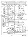
- a random access memory device is fabricated on a semiconductor substrate 41 and comprises a memory cell array 42, a plurality of bit line pairs BLP1 to BLPn, a plurality of sense amplifier circuits SA1 to SAn, a column selector circuit 43, a pair of input/output data signal lines 44a and 44b, a precharging circuit combined with an equalization circuit 44 provided for the bit line pairs BLP1 to BLPn, another precharging circuit combined with another equalization circuit 45 associated with the input/output data signal lines 44a and 44b, a pull-up circuit 46 coupled between a source of positive voltage level Vcc and the input/output data signal lines 44a and 44b, a row address decoder circuit 47, a column address decoder circuit 48, a data amplifier circuit 49, and a small n-channel type field effect transistor Q41 coupled between the input/output data signal lines 44a and 44b.
- the fifth current path is implemented by the n-channel type
- each of the memory cells is of the one-transistor and one-capacitor type and, accordingly, implemented by a series combination of a switching transistor Q42 and a storage capacitor C41.
- the switching transistors Q42 are of the n-channel type.
- the bit line pairs BLP1 to BLPn are respectively coupled to the columns of the memory cells M11 to Mmn and have first bit lines BL1 respectively paired with second bit lines BL2.
- the switching transistors Q42 in each column are alternately coupled to the first and second bit lines BL1 and BL2 of the associated bit line pair, and the storage capacitors C1 are coupled to a voltage supply line VL.
- a plurality of word lines W1 to Wm are coupled to the gate electrodes of the switching transistors Q42 of the rows, respectively, and the row address decoder circuit 47 drives one of the word lines W1 to Wm to an active high voltage level on the basis of row address bits.
- Each of the sense amplifier circuits SA1 to SAn comprises p-channel type field effect transistors Q43 and Q44 respectively coupled in series to n-channel type field effect transistors Q45 and Q46, and the two series combinations of the field effect transistors Q43 to Q46 are coupled in parallel between activation signal lines SAP and SANB.
- either p-channel type field effect transistor Q43 or Q44 provides the first current path
- either n-channel type field effect transistor Q45 or Q46 forms the second current path. Since the activation signal lines SAP and SANB are respectively shifted to a positive voltage level Vcc and a ground voltage level, the first and second current paths couple the first and second bit lines BL1 and BL2 with a source of positive voltage level and a source of the ground voltage level.
- the column selector circuit 43 comprises a plurality of switching transistors SW1a, SW1b, SWna and SWnb each formed by an n-channel type field effect transistor, and every two switching transistors SW1a and SW1b or SWna and SWnb are coupled at the gate electrodes thereof to one of the control lines extending in parallel from the column address decoder circuit 48. Every two switching transistors SW1a and SW1b or SWna and SWnb are associated with one of the bit line pairs BLP1 to BLPn and are coupled between the first and second bit lines BL1 and BL2 of the associated bit line pair and the input/output data signal lines 44a and 44b.
- the column address decoder circuit 48 drives one of the control lines to the positive voltage level Vcc, and, accordingly, the column selector circuit 43 interconnects one of the bit line pairs BLP1 to BLPn and the input/output data signal lines 44a and 44b.
- the precharging circuit combined with the precharging circuit 45 comprises a series combination of p-channel type field effect transistors Q47 and Q48 coupled between a source of precharging voltage level VCVT and the input/output data signal lines 44a and 44b, and a p-channel type field effect transistor Q49.
- the precharging voltage level VCVT is slightly lower than the positive voltage level Vcc.
- a precharging signal PIO is supplied to the gate electrodes of the p-channel type field effect transistors Q47 to Q49 so that the input/output data signal lines 44a and 44b are precharged to and balanced at the precharging voltage level VCVT.
- the pull-up circuit 46 is formed by two n-channel type field effect transistors Q50 and Q51 which are coupled in parallel between the source of positive voltage level Vcc and the input/output data signal lines 44a and 44b.
- the two n-channel type field effect transistors Q50 and Q51 provide the third and fourth current paths, respectively.
- a read mode signal RM is supplied to the gate electrodes of the n-channel type field effect transistors Q50 and Q51 so that the input/output data signal lines 44a and 44b alternately vary in voltage level within a predetermined voltage range.
- the precharging voltage level VCVT defines the upper voltage level of the predetermined voltage range, and the lower voltage level of the predetermined voltage range is determined by a ratio circuit constituted by the n-channel type field effect transistors Q50 (or Q51), one of the switching transistors SW1a to SWnb and the n-channel type field effect transistor Q45 (or Q46).
- the n-channel type field effect transistor Q50 or Q51 allows a pull-up current or a supplementary current to flow therethrough, and the amount of the pull-up current is tens to hundreds times larger than the amount of current passing through the n-channel type field effect transistor Q41.
- the n-channel type field effect transistors Q45, Q46 and SW1a to SWnb are as large in current driving capability as the n-channel type field effect transistors Q50 and Q51.
- the amount of the current flowing between the data signal lines 44a and 44b is much smaller than the pull-up current and, for this reason, hardly affects the read-out speed in a data read-out operation.
- the data read-out mode of operation is completed in tens nanosecond, fluctuation in voltage level at the source of voltage level Vcc continues at least several microsecond, and the small current path established in the n-channel type field effect transistor Q41 allows a data bit to be read out at a constant speed under fluctuation in voltage level.
- the random access memory device thus arranged selectively enters a data read-out mode of operation and a data write-in mode of operation.
- description is focused upon the data read-out mode of operation, because it would be easy to compare with the prior art semiconductor memory device. While no fluctuation in voltage level at the source of positive voltage level Vcc takes place, the random access memory device behaves as similar to the prior art semiconductor memory device shown in Fig. 1, and, therefore, description is omitted for avoiding repetition.
- the data bit of logic "1" level allows the input/output data signal line 44a to maintain in the upper voltage level of the predetermined voltage range, but the input/output data signal line 44b is decayed to the lower voltage level of the predetermined voltage range due to the second current path established in the n-channel type field effect transistor Q46 at time t6.
- the voltage level on the input/output data signal line 44b follows the positive voltage level Vcc to Vcc2 as shown in Fig. 5, because the voltage level on the input/output data signal line 44b is determined by the ratio circuit constituted by the transistors Q51, SW1b and Q46. Since the input/output data signal line 44a is conducted to the source of positive voltage level through the transistors SW1a and Q43, no current discharging path is coupled to the input/output data signal line 44a.
- the n-channel type field effect transistor Q41 is always turned on and allows the input/output data signal line 44a to follow the other input/output data signal line 44b. This results in that the voltage differences D11 and D12 are approximately equal to one another regardless of the fluctuation in voltage level. If the next column address bits designate other bit line pair with a data bit of logic "0" level, the column selector circuit 43 interconnects the other bit line pair and the input/output data signal lines 44a and 44b, and the other bit line pair alternates the voltage levels on the input/output data signal lines 44a and 44b with one another. However, the alternation in voltage level is achieved as quick as that under no fluctuation in voltage level, because the difference in voltage level D12 is as small as the difference D11.
- the n-channel type field effect transistor Q41 maintains the voltage difference between the input/output data signal lines 44a and 44b constant regardless of the fluctuation in voltage level, and, therefore, the random access memory device allows any external device to access a series of data bits at a constant speed under the fluctuation in voltage level at the source of positive voltage level Vcc.
- Fig. 6 of the drawings a random access memory device embodying the present invention is illustrated.
- the random access memory device shown in Fig. 6 is similar in circuit arrangement to that shown in Fig. 4 except for two additional field effect transistors Q61 and Q62, and, for this reason, the other component circuits and transistors are designated by the same reference numerals and marks used in Fig. 4.
- the two n-channel type field effect transistors Q61 and Q62 are coupled between the source of positive voltage level Vcc and the input/output data signal lines 44a and 44b, and the gate electrodes of the transistors Q61 and Q62 are coupled to the respective drain nodes thereof.
- the n-channel type field effect transistors Q61 and Q62 thus coupled serve as diodes and provide current paths from the input/output data signal lines 44a and 44b to the source of positive voltage level Vcc if the source of positive voltage is lower than the voltage levels on the input/output data signal lines 44a and 44b by a threshold voltage Vth of the transistors Q61 and Q62.
- the n-channel type field effect transistors Q61 and Q62 support the n-channel type field effect transistor Q41 upon violent voltage fluctuation exceeding the current driving capability of the transistor Q41, and, for this reason, the random access memory device shown in Fig. 6 is less affectable by fluctuation in voltage level rather than the random access memory device shown in Fig. 4.
- FIG. 7 another random access memory device has a resistor element 71.
- the resistor element 71 takes the position of the n-channel type field effect transistor Q41, but other component circuits and transistors are similar to those of the random access memory device shown in Fig. 4. For this reason, no further description is incorporated hereinbelow for the sake of simplicity.
- Fig. 8 shows still another random access memory device.
- the n-channel type field effect transistor Q41 is replaced with an n-channel type field effect transistor Q81 coupled in series with a resistor element 81.
- a resistor element 81 restricts the current passing through the n-channel type field effect transistor Q81, fabrication of the n-channel type field effect transistor Q81 is relatively easy rather than the fabrication of the n-channel type field effect transistor Q41. This enhances the production yield of the random access memory device.
- the fifth current path is established through the series combination of the n-channel type field effect transistor Q81 and the resistor element 81 and the current passing through the fifth current path is as small as that of the n-channel type field effect transistor Q41.
- the memory cell may have another circuit configuration such as a static random access memory cell.
- all of the preferred embodiments have the input/output data signal lines 44a and 44b; however, another implementation may have a pair of output data signal lines independent from a pair of input data signal lines.
Landscapes
- Engineering & Computer Science (AREA)
- Microelectronics & Electronic Packaging (AREA)
- Computer Hardware Design (AREA)
- Databases & Information Systems (AREA)
- Dram (AREA)
- Static Random-Access Memory (AREA)
Claims (1)
- Halbleiterspeichervorrichtung mit: a) einer Anzahl von Speicherzellen (M11/ Mm1/ M1n/ M1n), die in Zeilen und Spalten angeordnet sind und jeweils Datenbits speichern, b) einer Anzahl von Bitleitungspaaren (BLP1, BLPn), die jeweils mit den Spalten der Speicherzellen verbunden sind und erste Bitleitungen (BL1) und zweite Bitleitungen (BL2) aufweisen, die mit den ersten Bitleitungen jeweils gepaart sind, c) einer Anzahl von Wortleitungen (W1/ Wm), die jeweils mit den Zeilen der Speicherzellen verbunden sind und selektiv die Speicherzellen aktivieren, um kleine Differenzen im Spannungspegel auf der Anzahl von Bitleitungspaaren jeweils zu erzeugen, d) einer Anzahl von Leseverstärkerschaltungen (SA1/ SAn), die jeweils mit der Anzahl der Bitleitungspaare verbunden sind, wobei jede der Anzahl von Leseverstärkerschaltungen einen ersten Stromweg (Q43 oder Q44) zwischen einer ersten Spannungsquelle (Ycc) und einer der ersten und zweiten Bitleitungen schafft und einen zweiten Stromweg (Q45 oder Q46) zwischen einer zweiten Spannungsquelle und den anderen der ersten und zweiten Bitleitungen, abhängig von der geringen Differenz auf dem zugeordneten Bitleitungspaar, e) ersten und zweiten Datensignalleitungen (44a/ 44b), f) einer Spaltenauswahlschaltung (43), die die ersten und zweiten Datensignalleitungen und die ersten und zweiten Bitleitungen einer der Anzahl von Bitleitungspaaren miteinander verbindet, und g) einem dritten und einem vierten Stromweg (Q50/ Q51), die jeweils zwischen die erste Spannungsquelle (Vcc) und die erste und die zweite Datensignalleitung (44a/ 44b) geschaltet sind und Zusatzströme zu dem ersten bzw. dem zweiten Datensignalweg zuführt, um zu ermöglichen, daß die Spannungspegel auf der ersten und der zweiten Datensignalleitung innerhalb eines vorgegebenen Spannungsbereichs variieren, gekennzeichnet durch h) eine fünften Stromweg (Q41, 71, Q81/ 81), der zwischen die ersten und die zweiten Datensignalleitungen geschaltet ist und bewirkt, daß der Spannungspegel auf einer der ersten und zweiten Datensignalleitungen dem Spannungspegel auf der anderen der ersten und zweiten Datensignalleitungen folgt, um eine Potentialdifferenz zwischen ihnen im Fall von Fluktuationen des Spannungspegels in der ersten Spannungsquelle konstant zu halten, und i) einem sechsten und einem siebten Stromweg, die zwischen die erste Spannungsquelle (Vcc) und die erste und zweite Datensignalleitung (44a/ 44b) geschaltet sind und Transistoren (Q61, Q62) aufweisen, deren Gateelektroden mit ihren Drainknoten verbunden sind, so daß sie als Dioden arbeiten, die es einem Strom ermöglichen, von der ersten und der zweiten Datensignalleitung (44a/ 44b) zur ersten Spannungsquelle (Vcc) in Abhängigkeit von einer Fluktuation des Spannungspegels zu fließen.
Applications Claiming Priority (2)
| Application Number | Priority Date | Filing Date | Title |
|---|---|---|---|
| JP1299320A JPH03160689A (ja) | 1989-11-17 | 1989-11-17 | 半導体メモリ |
| JP299320/89 | 1989-11-17 |
Publications (3)
| Publication Number | Publication Date |
|---|---|
| EP0429018A2 EP0429018A2 (de) | 1991-05-29 |
| EP0429018A3 EP0429018A3 (en) | 1992-09-30 |
| EP0429018B1 true EP0429018B1 (de) | 1996-01-31 |
Family
ID=17871015
Family Applications (1)
| Application Number | Title | Priority Date | Filing Date |
|---|---|---|---|
| EP90121957A Expired - Lifetime EP0429018B1 (de) | 1989-11-17 | 1990-11-16 | Halbleiterspeicheranordnung mit Eingangs-/Ausgangs-Datensignalleitungen, die Bitinformation in Hochgeschwindigkeit übertragen unabhängig von der Schwankung des Speisespannungssignals |
Country Status (5)
| Country | Link |
|---|---|
| US (1) | US5124947A (de) |
| EP (1) | EP0429018B1 (de) |
| JP (1) | JPH03160689A (de) |
| KR (1) | KR940005685B1 (de) |
| DE (1) | DE69025133T2 (de) |
Families Citing this family (6)
| Publication number | Priority date | Publication date | Assignee | Title |
|---|---|---|---|---|
| JP2596180B2 (ja) * | 1990-05-28 | 1997-04-02 | 日本電気株式会社 | 半導体集積メモリ回路 |
| JP2748053B2 (ja) * | 1991-07-23 | 1998-05-06 | 三菱電機株式会社 | 半導体記憶装置 |
| JP2991546B2 (ja) * | 1991-10-07 | 1999-12-20 | 株式会社東芝 | 半導体集積回路 |
| KR0127263B1 (ko) * | 1993-02-23 | 1997-12-29 | 사토 후미오 | 반도체 집적회로 |
| DE4437493A1 (de) * | 1994-10-20 | 1996-04-25 | Werner Siegert | Laserstrahlgerät zur Rotationsnivellierung |
| US7471569B2 (en) * | 2005-06-15 | 2008-12-30 | Infineon Technologies Ag | Memory having parity error correction |
Family Cites Families (5)
| Publication number | Priority date | Publication date | Assignee | Title |
|---|---|---|---|---|
| JPS6032911B2 (ja) * | 1979-07-26 | 1985-07-31 | 株式会社東芝 | 半導体記憶装置 |
| JPS595989B2 (ja) * | 1980-02-16 | 1984-02-08 | 富士通株式会社 | スタティック型ランダムアクセスメモリ |
| JPS61237290A (ja) * | 1985-04-12 | 1986-10-22 | Sony Corp | ビツト線駆動回路 |
| US4740921A (en) * | 1985-10-04 | 1988-04-26 | Motorola, Inc. | Precharge of a dram data line to an intermediate voltage |
| JPH0642318B2 (ja) * | 1988-01-18 | 1994-06-01 | 株式会社東芝 | 半導体メモリ |
-
1989
- 1989-11-17 JP JP1299320A patent/JPH03160689A/ja active Pending
-
1990
- 1990-11-15 KR KR1019900018470A patent/KR940005685B1/ko not_active Expired - Fee Related
- 1990-11-16 EP EP90121957A patent/EP0429018B1/de not_active Expired - Lifetime
- 1990-11-16 DE DE69025133T patent/DE69025133T2/de not_active Expired - Fee Related
- 1990-11-19 US US07/615,738 patent/US5124947A/en not_active Expired - Fee Related
Also Published As
| Publication number | Publication date |
|---|---|
| KR910010518A (ko) | 1991-06-29 |
| DE69025133D1 (de) | 1996-03-14 |
| EP0429018A2 (de) | 1991-05-29 |
| JPH03160689A (ja) | 1991-07-10 |
| EP0429018A3 (en) | 1992-09-30 |
| DE69025133T2 (de) | 1996-07-18 |
| US5124947A (en) | 1992-06-23 |
| KR940005685B1 (ko) | 1994-06-22 |
Similar Documents
| Publication | Publication Date | Title |
|---|---|---|
| US5608667A (en) | Ferroelectric memory automatically generating biasing pulse for plate electrode | |
| US3949385A (en) | D.C. Stable semiconductor memory cell | |
| US7038938B2 (en) | Phase change resistor cell and nonvolatile memory device using the same | |
| KR920008245B1 (ko) | 불휘발성 반도체기억장치 | |
| US3993917A (en) | Parameter independent FET sense amplifier | |
| US5046050A (en) | Shared BiCMOS sense amplifier | |
| US5058072A (en) | Semiconductor memory device with high speed sensing facility | |
| US5568438A (en) | Sense amplifier with offset autonulling | |
| EP0264929A2 (de) | Halbleiterspeicheranordnung mit verbesserter Bitzeilenordnung | |
| US5323345A (en) | Semiconductor memory device having read/write circuitry | |
| KR100366012B1 (ko) | 안정된 셀 비를 갖는 고속 sram | |
| JP2939027B2 (ja) | 半導体記憶装置 | |
| US7286425B2 (en) | System and method for capacitive mis-match bit-line sensing | |
| US7782654B2 (en) | Static random access memory device | |
| KR20000057968A (ko) | 모든 메모리 셀에 의해 공유되는 워드선 구동 회로를구비하는 스태틱 램 | |
| US5148400A (en) | Semiconductor memory circuit having an improved restoring control circuit | |
| US4602355A (en) | Memory circuit with noise preventing means for word lines | |
| US5642314A (en) | Semiconductor integrated circuit | |
| KR930008575B1 (ko) | 저소비 전력 구성의 반도체 집적회로 장치 | |
| EP0429018B1 (de) | Halbleiterspeicheranordnung mit Eingangs-/Ausgangs-Datensignalleitungen, die Bitinformation in Hochgeschwindigkeit übertragen unabhängig von der Schwankung des Speisespannungssignals | |
| EP0503524B1 (de) | Halbleiterspeicheranordnung | |
| US4380055A (en) | Static RAM memory cell | |
| US6198681B1 (en) | Sense amplifier for low voltage memory arrays | |
| US4376987A (en) | Threshold referenced MNOS sense amplifier | |
| US4610002A (en) | Dynamic memory circuit with improved noise-prevention circuit arrangement for word lines |
Legal Events
| Date | Code | Title | Description |
|---|---|---|---|
| PUAI | Public reference made under article 153(3) epc to a published international application that has entered the european phase |
Free format text: ORIGINAL CODE: 0009012 |
|
| 17P | Request for examination filed |
Effective date: 19901116 |
|
| AK | Designated contracting states |
Kind code of ref document: A2 Designated state(s): DE FR GB |
|
| PUAL | Search report despatched |
Free format text: ORIGINAL CODE: 0009013 |
|
| AK | Designated contracting states |
Kind code of ref document: A3 Designated state(s): DE FR GB |
|
| 17Q | First examination report despatched |
Effective date: 19940627 |
|
| GRAA | (expected) grant |
Free format text: ORIGINAL CODE: 0009210 |
|
| AK | Designated contracting states |
Kind code of ref document: B1 Designated state(s): DE FR GB |
|
| REF | Corresponds to: |
Ref document number: 69025133 Country of ref document: DE Date of ref document: 19960314 |
|
| ET | Fr: translation filed | ||
| PLBE | No opposition filed within time limit |
Free format text: ORIGINAL CODE: 0009261 |
|
| STAA | Information on the status of an ep patent application or granted ep patent |
Free format text: STATUS: NO OPPOSITION FILED WITHIN TIME LIMIT |
|
| 26N | No opposition filed | ||
| PGFP | Annual fee paid to national office [announced via postgrant information from national office to epo] |
Ref country code: FR Payment date: 20011113 Year of fee payment: 12 |
|
| PGFP | Annual fee paid to national office [announced via postgrant information from national office to epo] |
Ref country code: GB Payment date: 20011114 Year of fee payment: 12 |
|
| PGFP | Annual fee paid to national office [announced via postgrant information from national office to epo] |
Ref country code: DE Payment date: 20011203 Year of fee payment: 12 |
|
| REG | Reference to a national code |
Ref country code: GB Ref legal event code: IF02 |
|
| PG25 | Lapsed in a contracting state [announced via postgrant information from national office to epo] |
Ref country code: GB Free format text: LAPSE BECAUSE OF NON-PAYMENT OF DUE FEES Effective date: 20021116 |
|
| PG25 | Lapsed in a contracting state [announced via postgrant information from national office to epo] |
Ref country code: DE Free format text: LAPSE BECAUSE OF NON-PAYMENT OF DUE FEES Effective date: 20030603 |
|
| GBPC | Gb: european patent ceased through non-payment of renewal fee | ||
| PG25 | Lapsed in a contracting state [announced via postgrant information from national office to epo] |
Ref country code: FR Free format text: LAPSE BECAUSE OF NON-PAYMENT OF DUE FEES Effective date: 20030731 |
|
| REG | Reference to a national code |
Ref country code: FR Ref legal event code: ST |