EP0429673A1 - Prüfmustergenerator - Google Patents
Prüfmustergenerator Download PDFInfo
- Publication number
- EP0429673A1 EP0429673A1 EP90909374A EP90909374A EP0429673A1 EP 0429673 A1 EP0429673 A1 EP 0429673A1 EP 90909374 A EP90909374 A EP 90909374A EP 90909374 A EP90909374 A EP 90909374A EP 0429673 A1 EP0429673 A1 EP 0429673A1
- Authority
- EP
- European Patent Office
- Prior art keywords
- test pattern
- control signal
- clock
- address
- read out
- Prior art date
- Legal status (The legal status is an assumption and is not a legal conclusion. Google has not performed a legal analysis and makes no representation as to the accuracy of the status listed.)
- Granted
Links
- 238000012360 testing method Methods 0.000 title claims abstract description 113
- 230000015654 memory Effects 0.000 claims abstract description 97
- 230000004044 response Effects 0.000 claims abstract description 5
- 239000004065 semiconductor Substances 0.000 abstract description 3
- 230000010354 integration Effects 0.000 abstract description 2
- 238000010586 diagram Methods 0.000 description 6
- 230000000717 retained effect Effects 0.000 description 2
- 230000006870 function Effects 0.000 description 1
- 230000000977 initiatory effect Effects 0.000 description 1
- 238000004519 manufacturing process Methods 0.000 description 1
- 238000000034 method Methods 0.000 description 1
- 238000000059 patterning Methods 0.000 description 1
- 230000003068 static effect Effects 0.000 description 1
- 230000001360 synchronised effect Effects 0.000 description 1
Images



Classifications
-
- G—PHYSICS
- G01—MEASURING; TESTING
- G01R—MEASURING ELECTRIC VARIABLES; MEASURING MAGNETIC VARIABLES
- G01R31/00—Arrangements for testing electric properties; Arrangements for locating electric faults; Arrangements for electrical testing characterised by what is being tested not provided for elsewhere
- G01R31/28—Testing of electronic circuits, e.g. by signal tracer
- G01R31/317—Testing of digital circuits
- G01R31/3181—Functional testing
- G01R31/319—Tester hardware, i.e. output processing circuits
- G01R31/31917—Stimuli generation or application of test patterns to the device under test [DUT]
- G01R31/31919—Storing and outputting test patterns
Definitions
- the present invention relates to a test pattern generator which generates test patterns for testing semiconductor integrated circuits.
- a test pattern generator forms a part of an IC tester for testing semiconductor ICs and generates a test pattern to be applied to the IC under test and an expected value pattern for comparison with a response from the IC under test. These two patterns are commonly referred to simply as a test pattern.
- a conventional test pattern generator is shown in Fig. 1.
- a clock PCK for pattern generating use and a start signal S are applied to an address generating circuit 11 and an address provided therefrom is used to read out a test pattern memory 12 in which a test pattern has been stored.
- the test pattern memory 12 is usually constituted by an SRAM (i.e. a static RAM).
- a large-capacity test pattern memory is needed to cope with extended test patterns which result from an increased degree of integration of circuits to be tested and an automatic generation of test patterns by a computer.
- a large-capacity test pattern memory employs the SRAM, and hence is expensive.
- the number of transistors necessary for forming one memory cell is four to six in the case of the SRAM but only one in the case of a DRAM (i.e. a dynamic RAM).
- a DRAM i.e. a dynamic RAM
- the IC memory using the DRAM is larger in capacity and lower in the unit cost per bit than the IC memory using the SRAM.
- the use of the DRAM will cut the manufacturing cost of the test pattern memory.
- stored contents of the DRAM will disappear unless refreshed at regular time intervals, and during the refresh the readout of a test pattern is suspended, making high-speed pattern generation impossible.
- the prior art does not employ the DRAM for the test pattern memory.
- the present invention is to provide a test pattern generator which can be fabricated at low cost through use of the DRAM and is capable of generating test patterns at high speed.
- a control circuit which operates on a system clock, is controlled by a start signal and a full flag to generate an address generating clock, a readout control signal and a write clock and, at the same time, a refresh control circuit is periodically provided from the control circuit.
- An address generating circuit is controlled by the address generating clock from the control circuit to generate an address.
- a test pattern memory formed by the DRAM and having stored therein test patterns is read out, based on the address from the address generating circuit and the readout control signal from the control circuit, and at the same time, the test pattern memory performs a refreshing operation based on the refresh control signal provided from the control circuit.
- the test pattern read out from the test pattern memory is written into a FiFo memory by the write clock from the control circuit. When filled with test patterns, the FiFo memory provides a full flag to the control circuit and the test patterns are read out from the FiFo memory in synchronism with the pattern generating clock.
- the address generating clock is made higher in rate than the pattern generating clock.
- test patterns can be read out of the FiFo memory continuously and hence at high speed without being affected by the refreshing operation of the test pattern memory.
- Fig. 2 illustrates an embodiment of the test pattern generator according to the present invention.
- the test pattern generator of the present invention comprises a control circuit 21, a FiFo memory 22, an address generating circuit 31 and a DRAM 32 serving as a test pattern memory, and is supplied with a system clock SCK, a pattern generating clock PCK and a start signal S from a control section of an IC tester (not shown) to perform a test pattern generating operation.
- the control circuit 21 is synchronized with the system clock to generate a refresh control signal REF, an address generating clock ACK, a readout control signal RC and a write clock WCK with predetermined periods, respectively, but during its generation of the refresh control signal REF and during the input thereinto of a full flag FF from the FiFo memory 22, the control circuit does not generate the address generating clock, the readout control signal and the write clock.
- the control circuit 21 is made up of a timing generating circuit 23, a full flag rise detector circuit 24R, a full flag fall detector circuit 24F, a flip-flop 25 and AND gates 26 to 29, as depicted in Fig. 3.
- the timing generator 23 generates the address generating clock ACK, the readout control signal RC, the write clock WCK and the refresh control signal REF on predetermined periods, respectively, and in synchronism with the system clock SCK and applies the first three signals to the AND gates 27 to 29 at one input thereof and provides the refresh control signal REF, as an inhibit signal, to the AND gate 26 and, at the same time, applies it to the test pattern memory 32.
- the flip-flop 25 is set by the start signal S and its Q output goes high and is provided, as an enable signal EN, via the AND gate 26 to the other inputs of the AND gates 27 to 29 to enable these gates, through which the address generating clock ACK, the readout control signal RC and the write clock WCK are output.
- the full flag FF is applied from the FiFo memory 22
- its leading edge is detected by the full flag rise detector 24R and its detected output is used to reset the flip-flop 25; so that the enable signal EN goes low and the gates 27 to 29 are disabled, stopping the outputting of the address generating clock ACK, the readout control signal RC and the write clock WCK.
- the address generating clock ACK from the control circuit 21 is applied to the address generator 31, which, in turn, generates addresses A0, A1, A2, ... one by one upon each application of the address generating clock ACK.
- the addresses thus obtained and the readout control signal RC from the control circuit 21 are used to read out test patterns P0, P1, P2, ... from the test pattern memory 32.
- the test pattern memory 32 is formed by a DRAM, which has stored therein test patterns and performs the refresh operation when supplied with the refresh control signal REF from the control circuit 21.
- the test patterns P0, P1, P2, ... read out of the test pattern memory 32 are written into the FiFo memory 22 by the write clock WCK provided from the control circuit.
- the FiFo memory 22 provides the full flag FF to the control circuit 21.
- Ordinary FiFo memories have a full flag generating function.
- the FiFo memory 22 is read out in synchronism with the pattern generating clock PCK.
- the readout of the FiFo memory 22 starts with old data.
- the rate of the pattern generating clock PCK is made higher than the rate of the address generating clock ACK. More specifically, letting the period of the pattern generating clock PCK, the readout period of the test pattern memory 32 (i.e.
- the period of the address generating clock ACK) and the time for refreshing the test pattern memory 32 be represented by T1, T2 and Tr, respectively, and assuming that the test pattern memory 32 is refreshed every m-th readout therefrom, the period T2 is chosen so that the following relationship holds: m x T1 > m x T2 + Tr (1 )
- the flip-flop 25 is set to make the enable signal EN high, by which the gates 27 to 29 are enabled, starting the output of the address generating clock ACK.
- the addresses A0, A1, A2, ... are produced one after another by the address generator 31, and at the same time, the control circuit 21 starts to generate the readout control signal RC, and the test patterns P0, P1, P2, are sequentially read out of the test pattern memory 32 and then written into the FiFo memory 22 by the write clock WCK.
- the full flag FF rises, by which the flip-flop 25 is reset and the enable signal EN goes low.
- the gates 27, 28 and 29 inhibit the passage therethrough of the address generating clock ACK, the readout control signal RC and the write clock WCK, respectively, and the readout of the test pattern memory 32 is stopped.
- the write into the FiFo memory 22 is also stopped.
- the readout of the test pattern memory 32 by an address A h being generated by the address generator 31 at that time is not performed and the address A h is retained.
- the pattern generating clock PCK is input in this state and the FiFo memory 22 is read out in synchronism with the clock PCK, providing the test patterns P0, P1, P2, ...
- the full flag FF falls, by which the flip-flop 25 is set.
- the enable signal EN goes high again and the readout of the test pattern memory 32 by the retained address A h is resumed and the write into the FiFo memory 22 is also resumed.
- the test pattern memory 32 When supplied with the refresh control signal REF from the control circuit 21, the test pattern memory 32 performs the refresh operation. Since the gate 26 is kept disabled during the refresh of the test pattern memory 32, the enable signal EN goes low and the gates 27, 28 and 29 inhibit the passage therethrough of the address generating clock ACK, the readout control signal RC and the write clock WCK, respectively.
- the address generator 31 retains an address A j that it is generating at that time, and the write into the FiFo memory 22 is also stopped, but the readout of the FiFo memory 22 by the pattern generating clock PCK is continued; so that output test patterns are continuously obtained.
- the gate 26 Upon completion of the refresh operation of the test pattern memory 32, the gate 26 is enabled and the readout of the test pattern memory 32 is resumed by the address A j and the write into the FiFo memory 22 is also resumed.
- the test pattern memory 32 Since the average readout rate of the test pattern memory 32, including the refresh period, is higher than the readout rate of the FiFo memory 22, the memory 22 becomes full until the refresh control signal REF is generated next. Thus, the test patterns can be continuously read out from the FiFo memory 22.
- test pattern memories 32-1 to 32-N are provided for one FiFo memory 22 and are simultaneously operated by the addresses A0, A1, ..., the readout control signal RC and the refresh control signal REF common to them and test patterns thus read out of the N test pattern memories are taken out by a multiplexer 33 sequentially and cyclically and written into the FiFo memory 22.
- the control circuit 21 needs only to have an arrangement in which the system clock SCK of the period T2 is repeatedly counted from 0 to N-1 by an N-ary counter in the timing generator 23 in Fig. 3 and the count values are sequentially output as a select signal SEL and a signal of a period N x T2 and a desired phase, obtained by detecting a desired count value of the N-ary counter through use of a decoder, is output as the address generating clock ACK, the readout control signal RC and the write clock WCK.
- the period T2 of the system clock SCK is so selected as to satisfy Eq. (1).
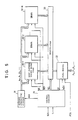
- test patterns at high speed by using such an arrangement as shown in Fig. 6, in which N test pattern memories 32-1 to 32-N and N FiFo memories 22-1 to 22-N are provided in combination and are concurrently operated by the addresses, the readout control signal RC, the refresh control signal REF and the write clock WCK common to them and test patterns thus read out of the N FiFo memories by readout clocks RCK-1 to RCK-N are taken out by the multiplexer 33 sequentially and cyclically.
- a control circuit 21-1 may be the same as that shown in Fig. 3.
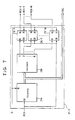
- a control circuit 21-2 is composed of an N-ary counter 21A, a decoder 21B and N flip-flops 21C-1 to 21C-N, as depicted in Fig. 7.
- the N-ary counter 21A and the flip-flops 21C-1 to 21C-N are reset by the start signal S.
- the N-ary counter 21A repeatedly counts the pattern generating clock PCK from 0 to N-1.
- the decoder has N output terminals and provides high-level outputs to its output terminals 1 to N one after another as the count value of the counter 21A varies from 0 to N-1 in a sequential order.
- the outputs of the decoder 21B are respectively taken into the flip-flops 21C-1 to 21C-N in synchronism with the pattern generating clock PCK and their Q outputs sequentially go high for one cycle period of the clock PCK.
- Such Q outputs of the flip-flops are used as readout clocks RCK-1 to RCK-N of the FiFo memories 22-1 to 22-N.
- the count value of the counter 21A is provided as the select signal SEL to the multiplexer 33.
- test patterns can continuously be obtained from the FiFo memory even during the refresh of the DRAM, since the test pattern generator has an arrangement in which test patterns read out of the test pattern memory formed by the DRAM are written into the FiFo memory which is read out by the pattern generating clock. Since the test pattern memory is formed by the DRAM, even an extended pattern can be produced by a low-cost device.
Landscapes
- Engineering & Computer Science (AREA)
- General Engineering & Computer Science (AREA)
- Physics & Mathematics (AREA)
- General Physics & Mathematics (AREA)
- For Increasing The Reliability Of Semiconductor Memories (AREA)
- Tests Of Electronic Circuits (AREA)
- Dram (AREA)
Applications Claiming Priority (3)
| Application Number | Priority Date | Filing Date | Title |
|---|---|---|---|
| JP154097/89 | 1989-06-16 | ||
| JP15409789 | 1989-06-16 | ||
| PCT/JP1990/000767 WO1990015999A1 (fr) | 1989-06-16 | 1990-06-13 | Generateur de mire electronique |
Publications (3)
| Publication Number | Publication Date |
|---|---|
| EP0429673A1 true EP0429673A1 (de) | 1991-06-05 |
| EP0429673A4 EP0429673A4 (en) | 1992-07-01 |
| EP0429673B1 EP0429673B1 (de) | 1996-11-13 |
Family
ID=15576849
Family Applications (1)
| Application Number | Title | Priority Date | Filing Date |
|---|---|---|---|
| EP90909374A Expired - Lifetime EP0429673B1 (de) | 1989-06-16 | 1990-06-13 | Prüfmustergenerator |
Country Status (5)
| Country | Link |
|---|---|
| US (1) | US5265102A (de) |
| EP (1) | EP0429673B1 (de) |
| JP (1) | JP2936547B2 (de) |
| DE (1) | DE69029122T2 (de) |
| WO (1) | WO1990015999A1 (de) |
Cited By (2)
| Publication number | Priority date | Publication date | Assignee | Title |
|---|---|---|---|---|
| DE19502828A1 (de) * | 1994-02-09 | 1995-08-10 | Advantest Corp | Mustergenerator für ein Halbleiter-Testgerät |
| EP0699999A3 (de) * | 1994-09-01 | 1996-11-27 | Teradyne Inc | Speicherarchitektur für eine automatische Testeinrichtung mit Vektormodultabelle |
Families Citing this family (30)
| Publication number | Priority date | Publication date | Assignee | Title |
|---|---|---|---|---|
| US5349587A (en) * | 1992-03-26 | 1994-09-20 | Northern Telecom Limited | Multiple clock rate test apparatus for testing digital systems |
| US5815512A (en) * | 1994-05-26 | 1998-09-29 | Mitsubishi Denki Kabushiki Kaisha | Semiconductor memory testing device |
| JPH0862302A (ja) * | 1994-08-19 | 1996-03-08 | Advantest Corp | サイクル遅延用パターン発生器 |
| US5805471A (en) * | 1994-11-01 | 1998-09-08 | Pycon, Inc. | Driver board apparatus having SRAM and burn-in system and method using host computer |
| TW358907B (en) * | 1994-11-22 | 1999-05-21 | Monolithic System Tech Inc | A computer system and a method of using a DRAM array as a next level cache memory |
| WO1996016371A1 (en) * | 1994-11-22 | 1996-05-30 | Monolithic System Technology, Inc. | Method and structure for utilizing a dram array as second level cache memory |
| JPH08184648A (ja) * | 1994-12-28 | 1996-07-16 | Advantest Corp | 半導体試験装置用テストパターンの高速転送装置 |
| US6128700A (en) * | 1995-05-17 | 2000-10-03 | Monolithic System Technology, Inc. | System utilizing a DRAM array as a next level cache memory and method for operating same |
| JPH1073643A (ja) * | 1996-09-02 | 1998-03-17 | Mitsubishi Electric Corp | 半導体装置試験治具 |
| US6249533B1 (en) | 1996-11-29 | 2001-06-19 | Advantest Corporation | Pattern generator |
| JP3233068B2 (ja) * | 1997-05-23 | 2001-11-26 | 安藤電気株式会社 | パターン発生装置 |
| US6272588B1 (en) * | 1997-05-30 | 2001-08-07 | Motorola Inc. | Method and apparatus for verifying and characterizing data retention time in a DRAM using built-in test circuitry |
| US6161206A (en) * | 1998-04-30 | 2000-12-12 | Credence Systems Corporation | Pattern generator for a semiconductor integrated circuit tester |
| US6651203B1 (en) * | 1999-05-17 | 2003-11-18 | Infineon Technologies Ag | On chip programmable data pattern generator for semiconductor memories |
| US6321356B1 (en) * | 1999-05-18 | 2001-11-20 | Micron Technology, Inc. | Programmable pattern generator |
| US6671845B1 (en) * | 1999-10-19 | 2003-12-30 | Schlumberger Technologies, Inc. | Packet-based device test system |
| KR100474421B1 (ko) * | 2000-08-31 | 2005-03-14 | 엔이씨 일렉트로닉스 가부시키가이샤 | 반도체 기억 장치 및 그 테스트 방법과 테스트 회로 |
| US6598112B1 (en) * | 2000-09-11 | 2003-07-22 | Agilent Technologies, Inc. | Method and apparatus for executing a program using primary, secondary and tertiary memories |
| US7062697B2 (en) * | 2000-12-07 | 2006-06-13 | Youngtek Electronics Corporation | Pre-stored digital word generator |
| KR100929336B1 (ko) | 2001-03-29 | 2009-12-03 | 파나소닉 주식회사 | 데이터를 암호화하여 데이터를 보호하는 데이터 보호 시스템 |
| US7106227B2 (en) * | 2001-09-28 | 2006-09-12 | Agilent Technologies, Inc. | Method and apparatus for synchronizing a multiple-stage multiplexer |
| US7073100B2 (en) * | 2002-11-11 | 2006-07-04 | International Business Machines Corporation | Method for testing embedded DRAM arrays |
| JP4237109B2 (ja) * | 2004-06-18 | 2009-03-11 | エルピーダメモリ株式会社 | 半導体記憶装置及びリフレッシュ周期制御方法 |
| US7321521B2 (en) | 2004-07-02 | 2008-01-22 | Seagate Technology Llc | Assessing energy requirements for a refreshed device |
| US7177222B2 (en) * | 2005-03-04 | 2007-02-13 | Seagate Technology Llc | Reducing power consumption in a data storage system |
| US20070050668A1 (en) * | 2005-09-01 | 2007-03-01 | Micron Technology, Inc. | Test mode to force generation of all possible correction codes in an ECC memory |
| JP5220639B2 (ja) * | 2009-01-29 | 2013-06-26 | 日本エンジニアリング株式会社 | テスト信号生成装置 |
| US8448008B2 (en) * | 2009-03-27 | 2013-05-21 | Mentor Graphics Corporation | High speed clock control |
| US8233919B2 (en) | 2009-08-09 | 2012-07-31 | Hntb Holdings Ltd. | Intelligently providing user-specific transportation-related information |
| KR102849290B1 (ko) | 2020-08-21 | 2025-08-25 | 삼성전자주식회사 | 반도체 장치 및 메모리 시스템 |
Family Cites Families (14)
| Publication number | Priority date | Publication date | Assignee | Title |
|---|---|---|---|---|
| JPS5439980B2 (de) * | 1972-03-24 | 1979-11-30 | ||
| US3982111A (en) * | 1975-08-04 | 1976-09-21 | Bell Telephone Laboratories, Incorporated | Memory diagnostic arrangement |
| US4451918A (en) * | 1981-10-09 | 1984-05-29 | Teradyne, Inc. | Test signal reloader |
| JPS59204782A (ja) * | 1983-05-10 | 1984-11-20 | Nec Corp | 試験パタ−ン発生装置 |
| JPS59207495A (ja) * | 1983-05-11 | 1984-11-24 | Hitachi Ltd | パタ−ン発生回路 |
| US4622668A (en) * | 1984-05-09 | 1986-11-11 | International Business Machines Corporation | Process and apparatus for testing a microprocessor and dynamic ram |
| US4727312A (en) * | 1985-12-23 | 1988-02-23 | Genrad, Inc. | Circuit tester |
| JPS63183696A (ja) * | 1987-01-23 | 1988-07-29 | Nec Corp | メモリ装置 |
| US4827476A (en) * | 1987-04-16 | 1989-05-02 | Tandem Computers Incorporated | Scan test apparatus for digital systems having dynamic random access memory |
| JPS63265181A (ja) * | 1987-04-22 | 1988-11-01 | Nec Corp | フアンクシヨンテスタ |
| US4782487A (en) * | 1987-05-15 | 1988-11-01 | Digital Equipment Corporation | Memory test method and apparatus |
| US4980888A (en) * | 1988-09-12 | 1990-12-25 | Digital Equipment Corporation | Memory testing system |
| JPH0255331U (de) * | 1988-10-11 | 1990-04-20 | ||
| JPH02195599A (ja) * | 1989-01-24 | 1990-08-02 | Ricoh Co Ltd | 情報処理装置 |
-
1990
- 1990-06-13 EP EP90909374A patent/EP0429673B1/de not_active Expired - Lifetime
- 1990-06-13 WO PCT/JP1990/000767 patent/WO1990015999A1/ja not_active Ceased
- 1990-06-13 US US07/655,364 patent/US5265102A/en not_active Expired - Lifetime
- 1990-06-13 JP JP15471090A patent/JP2936547B2/ja not_active Expired - Fee Related
- 1990-06-13 DE DE69029122T patent/DE69029122T2/de not_active Expired - Fee Related
Cited By (4)
| Publication number | Priority date | Publication date | Assignee | Title |
|---|---|---|---|---|
| DE19502828A1 (de) * | 1994-02-09 | 1995-08-10 | Advantest Corp | Mustergenerator für ein Halbleiter-Testgerät |
| DE19502828C2 (de) * | 1994-02-09 | 1999-04-29 | Advantest Corp | Testmustergenerator für ein Halbleiterschaltungs-Testgerät |
| EP0699999A3 (de) * | 1994-09-01 | 1996-11-27 | Teradyne Inc | Speicherarchitektur für eine automatische Testeinrichtung mit Vektormodultabelle |
| US6286120B1 (en) | 1994-09-01 | 2001-09-04 | Teradyne, Inc. | Memory architecture for automatic test equipment using vector module table |
Also Published As
| Publication number | Publication date |
|---|---|
| EP0429673B1 (de) | 1996-11-13 |
| JPH0394182A (ja) | 1991-04-18 |
| DE69029122T2 (de) | 1997-04-03 |
| US5265102A (en) | 1993-11-23 |
| EP0429673A4 (en) | 1992-07-01 |
| DE69029122D1 (de) | 1996-12-19 |
| WO1990015999A1 (fr) | 1990-12-27 |
| JP2936547B2 (ja) | 1999-08-23 |
Similar Documents
| Publication | Publication Date | Title |
|---|---|---|
| EP0429673A1 (de) | Prüfmustergenerator | |
| US4835774A (en) | Semiconductor memory test system | |
| EP0519584B1 (de) | Halbleiterspeicher | |
| US4667330A (en) | Semiconductor memory device | |
| US7573778B2 (en) | Semiconductor memory device | |
| EP0620556A2 (de) | Halbleiterspeichergerät mit Register zum Halten eines Prüfergebnisssignals | |
| JPH08297999A (ja) | 自己試験機能を有するdram | |
| US5414672A (en) | Semiconductor memory device including address transition detector | |
| US5111433A (en) | Semiconductor memory device with inhibiting test mode cancellation and operating method thereof | |
| KR100211609B1 (ko) | 이중에지 클록을 사용한 집적회로 소자 검사방법 | |
| KR100591760B1 (ko) | 가변 가능한 메모리 사이즈를 갖는 반도체 메모리 장치 | |
| EP0239916A2 (de) | Halbleiterspeichervorrichtung mit einem Testmodus und einem Standardmodusbetrieb | |
| US4347589A (en) | Refresh counter test | |
| EP0019150B1 (de) | Verfahren und Schaltung zum Prüfen der Arbeitsweise eines internen Regenerierungszählers in einem Speicher mit wahlfreiem Zugriff | |
| US6317373B1 (en) | Semiconductor memory device having a test mode and semiconductor testing method utilizing the same | |
| US5897653A (en) | Data tracing apparatus | |
| US5327387A (en) | Dynamic random access memory having an improved operational stability | |
| KR0121776B1 (ko) | 동기식 디램의 히든 셀프 리프레쉬 장치 | |
| JPH0778498A (ja) | 半導体メモリ装置およびその検査方法 | |
| JPH11283397A (ja) | 半導体記憶装置とその試験方法 | |
| KR960009947B1 (ko) | 디램의 리프레쉬 회로 | |
| KR970007525B1 (ko) | 어드레스 프로세싱 회로와 이를 이용한 반도체 기억장치 | |
| JP3018431B2 (ja) | 半導体メモリ用オンチップテスト方式 | |
| KR940008725B1 (ko) | 반도체 메모리 장치의 테스트 방법 및 회로 | |
| JPH07141861A (ja) | ダイナミックメモリ |
Legal Events
| Date | Code | Title | Description |
|---|---|---|---|
| PUAI | Public reference made under article 153(3) epc to a published international application that has entered the european phase |
Free format text: ORIGINAL CODE: 0009012 |
|
| 17P | Request for examination filed |
Effective date: 19910212 |
|
| AK | Designated contracting states |
Kind code of ref document: A1 Designated state(s): DE FR GB NL |
|
| A4 | Supplementary search report drawn up and despatched |
Effective date: 19920508 |
|
| AK | Designated contracting states |
Kind code of ref document: A4 Designated state(s): DE FR GB NL |
|
| 17Q | First examination report despatched |
Effective date: 19941115 |
|
| GRAG | Despatch of communication of intention to grant |
Free format text: ORIGINAL CODE: EPIDOS AGRA |
|
| GRAH | Despatch of communication of intention to grant a patent |
Free format text: ORIGINAL CODE: EPIDOS IGRA |
|
| GRAH | Despatch of communication of intention to grant a patent |
Free format text: ORIGINAL CODE: EPIDOS IGRA |
|
| GRAA | (expected) grant |
Free format text: ORIGINAL CODE: 0009210 |
|
| AK | Designated contracting states |
Kind code of ref document: B1 Designated state(s): DE FR GB NL |
|
| REF | Corresponds to: |
Ref document number: 69029122 Country of ref document: DE Date of ref document: 19961219 |
|
| ET | Fr: translation filed | ||
| PLBE | No opposition filed within time limit |
Free format text: ORIGINAL CODE: 0009261 |
|
| STAA | Information on the status of an ep patent application or granted ep patent |
Free format text: STATUS: NO OPPOSITION FILED WITHIN TIME LIMIT |
|
| 26N | No opposition filed | ||
| PGFP | Annual fee paid to national office [announced via postgrant information from national office to epo] |
Ref country code: NL Payment date: 19990603 Year of fee payment: 10 |
|
| PG25 | Lapsed in a contracting state [announced via postgrant information from national office to epo] |
Ref country code: NL Free format text: LAPSE BECAUSE OF NON-PAYMENT OF DUE FEES Effective date: 20010101 |
|
| NLV4 | Nl: lapsed or anulled due to non-payment of the annual fee |
Effective date: 20010101 |
|
| REG | Reference to a national code |
Ref country code: GB Ref legal event code: IF02 |
|
| PGFP | Annual fee paid to national office [announced via postgrant information from national office to epo] |
Ref country code: FR Payment date: 20020422 Year of fee payment: 13 |
|
| PGFP | Annual fee paid to national office [announced via postgrant information from national office to epo] |
Ref country code: GB Payment date: 20020612 Year of fee payment: 13 |
|
| PG25 | Lapsed in a contracting state [announced via postgrant information from national office to epo] |
Ref country code: GB Free format text: LAPSE BECAUSE OF NON-PAYMENT OF DUE FEES Effective date: 20030613 |
|
| GBPC | Gb: european patent ceased through non-payment of renewal fee |
Effective date: 20030613 |
|
| PG25 | Lapsed in a contracting state [announced via postgrant information from national office to epo] |
Ref country code: FR Free format text: LAPSE BECAUSE OF NON-PAYMENT OF DUE FEES Effective date: 20040227 |
|
| REG | Reference to a national code |
Ref country code: FR Ref legal event code: ST |
|
| PGFP | Annual fee paid to national office [announced via postgrant information from national office to epo] |
Ref country code: DE Payment date: 20070607 Year of fee payment: 18 |
|
| PG25 | Lapsed in a contracting state [announced via postgrant information from national office to epo] |
Ref country code: DE Free format text: LAPSE BECAUSE OF NON-PAYMENT OF DUE FEES Effective date: 20090101 |