EP0430044A2 - Verfahren zur Steuerung eines Wechselrichters - Google Patents
Verfahren zur Steuerung eines Wechselrichters Download PDFInfo
- Publication number
- EP0430044A2 EP0430044A2 EP90122213A EP90122213A EP0430044A2 EP 0430044 A2 EP0430044 A2 EP 0430044A2 EP 90122213 A EP90122213 A EP 90122213A EP 90122213 A EP90122213 A EP 90122213A EP 0430044 A2 EP0430044 A2 EP 0430044A2
- Authority
- EP
- European Patent Office
- Prior art keywords
- inverter
- phase
- switching elements
- voltage
- pulse mode
- Prior art date
- Legal status (The legal status is an assumption and is not a legal conclusion. Google has not performed a legal analysis and makes no representation as to the accuracy of the status listed.)
- Granted
Links
Images


Classifications
-
- H—ELECTRICITY
- H02—GENERATION; CONVERSION OR DISTRIBUTION OF ELECTRIC POWER
- H02M—APPARATUS FOR CONVERSION BETWEEN AC AND AC, BETWEEN AC AND DC, OR BETWEEN DC AND DC, AND FOR USE WITH MAINS OR SIMILAR POWER SUPPLY SYSTEMS; CONVERSION OF DC OR AC INPUT POWER INTO SURGE OUTPUT POWER; CONTROL OR REGULATION THEREOF
- H02M7/00—Conversion of AC power input into DC power output; Conversion of DC power input into AC power output
- H02M7/42—Conversion of DC power input into AC power output without possibility of reversal
- H02M7/44—Conversion of DC power input into AC power output without possibility of reversal by static converters
- H02M7/48—Conversion of DC power input into AC power output without possibility of reversal by static converters using discharge tubes with control electrode or semiconductor devices with control electrode
- H02M7/483—Converters with outputs that each can have more than two voltages levels
- H02M7/487—Neutral point clamped inverters
-
- H—ELECTRICITY
- H02—GENERATION; CONVERSION OR DISTRIBUTION OF ELECTRIC POWER
- H02M—APPARATUS FOR CONVERSION BETWEEN AC AND AC, BETWEEN AC AND DC, OR BETWEEN DC AND DC, AND FOR USE WITH MAINS OR SIMILAR POWER SUPPLY SYSTEMS; CONVERSION OF DC OR AC INPUT POWER INTO SURGE OUTPUT POWER; CONTROL OR REGULATION THEREOF
- H02M7/00—Conversion of AC power input into DC power output; Conversion of DC power input into AC power output
- H02M7/42—Conversion of DC power input into AC power output without possibility of reversal
- H02M7/44—Conversion of DC power input into AC power output without possibility of reversal by static converters
- H02M7/48—Conversion of DC power input into AC power output without possibility of reversal by static converters using discharge tubes with control electrode or semiconductor devices with control electrode
- H02M7/483—Converters with outputs that each can have more than two voltages levels
- H02M7/4837—Flying capacitor converters
-
- H—ELECTRICITY
- H02—GENERATION; CONVERSION OR DISTRIBUTION OF ELECTRIC POWER
- H02P—CONTROL OR REGULATION OF ELECTRIC MOTORS, ELECTRIC GENERATORS OR DYNAMO-ELECTRIC CONVERTERS; CONTROLLING TRANSFORMERS, REACTORS OR CHOKE COILS
- H02P27/00—Arrangements or methods for the control of AC motors characterised by the kind of supply voltage
- H02P27/04—Arrangements or methods for the control of AC motors characterised by the kind of supply voltage using variable-frequency supply voltage, e.g. inverter or converter supply voltage
- H02P27/06—Arrangements or methods for the control of AC motors characterised by the kind of supply voltage using variable-frequency supply voltage, e.g. inverter or converter supply voltage using DC to AC converters or inverters
- H02P27/08—Arrangements or methods for the control of AC motors characterised by the kind of supply voltage using variable-frequency supply voltage, e.g. inverter or converter supply voltage using DC to AC converters or inverters with pulse width modulation
- H02P27/14—Arrangements or methods for the control of AC motors characterised by the kind of supply voltage using variable-frequency supply voltage, e.g. inverter or converter supply voltage using DC to AC converters or inverters with pulse width modulation with three or more levels of voltage
Definitions
- This invention relates to a three-phase three-level inverter for use in an electric railcar or the like.
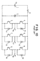
- a type of three-phase two-level inverter such as that shown in Fig. 10 has been used for inverter electric railcars.
- This inverter operates in a constant-V/f control mode called a three-pulse mode in the range of inverter frequencies lower than a predetermined frequency.
- This mode is based on a synchronous pulse width modulation method in which sinusoidal waves and a triangular wave are compared and, in this mode, the frequency of the triangular wave is three times as those of the sinusoidal waves.
- the inverter operates in a whole voltage control mode called a one-pulse mode.
- the inverter has a DC power source 1, a reactor 2 connected to a plus terminal of the DC power source 1, and a capacitor 3 connected between the reactor 2 and a minus terminal of the DC power source 1.
- Three pairs of switching elements 4-5, 6-7, and 8-9 each connected in series are connected in parallel with the capacitor 3.
- Free-wheeling diodes 10 to 15 are connected in parallel with the respective switching elements 4 to 9 with reverse polarities.
- a phase-in output terminal 16, a phase-V output terminal 17 and a phase-W output terminal 18 extend from middle points between the pairs of switching elements.
- the reactor 2 and the capacitor 3 form a DC filter, and each of the switching elements 4 to 9 is a GTO thyristor, a power transistor or the like.
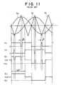
- a phase-in output voltage V U is obtained from a phase-U sinusoidal modulating wave S U and a triangular carrier wave S C
- a phase-V output voltage V V is obtained from a phase-V sinusoidal modulating wave S V and the triangular carrier wave S C
- the line U-V voltage V UV1 is exhibited as a rectangular wave having a width of 120°.
- the ratio of the amplitude of each phase sinusoidal modulating wave to the amplitude of the triangular carrier wave S C i.e., the percentage modulation is changed to control the angle ⁇ which is determined by the points of intersection of each phase sinusoidal modulating wave and the triangular carrier wave S C as shown in Fig. 11, thereby changing the line U-V voltage V UV .
- the angle ⁇ has a minimum value ⁇ min > 0 depending upon restrictions owing to the minimum switching element off time, setting of a period of time for preventing short-circuit of upper and lower arms of the inverter unit, and so on.
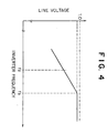
- the line voltage V UV1 in the one-pulse mode forms a 120° width rectangular wave, as mentioned above.
- the line voltage is abruptly increased by a step corresponding to the width ⁇ slit. That is, referring to Fig. 12, when the inverter operates for change-over from the three-pulse mode to the one-pulse mode at the inverter frequency f0, change-over is actually effected at an inverter frequency f1.
- the dot- dash line indicates the change in the line voltage in an ideal state.
- a discontinuous change in the line voltage of about 10 % occurs at the time of transition from three-pulse mode operation to one-phase mode operation, resulting in occurrence of an undesirable phenomenon such as an abrupt change in the inverter output current or output torque or voltage oscillation of the DC filter.
- an object of the present invention to provide an inverter control method capable of smoothly controlling the line voltage of an inverter without reducing the voltage utilization coefficient.
- An inverter control method in accordance with the present invention is a method of controlling the output voltage of a three-phase three-level inverter having a plurality of switching elements by pulse width modulation. This method comprises setting the upper limit of the percentage modulation to a value equal to or smaller than the maximum percentage modulation determined by the minimum off time of the switching elements, and outputting a three-level voltage as an inverter output voltage in each phase if each of the switching element is turned on and off one time during one inverter output period.
- the three-phase three-level inverter effects pulse width modulation even in the one-pulse mode to prevent the line voltage from changing discontinuously at the time of transition from the three-pulse mode to the one-pulse mode, which phenomenon cannot be avoided by the conventional method, thereby continuously changing the line voltage. If the percentage modulation is increased to the maximum value determined by the minimum switching element off time, the voltage utilization coefficient is substantially the same as that attained by the conventional method in the one-pulse mode.
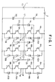
- An inverter shown in Fig. 1 is a three-phase three-level inverter having a DC power source 1, a reactor 2 connected to a plus terminal of the DC power source 1, and a pair of capacitors 3A and 3B connected in series between the reactor 2 and a minus terminal of the DC power source 1.
- the inverter also has first to sixth pairs of switching elements 4A-4B, 5A-5B, 6A-6B, 7A-7B, 8A-8B, and 9A-9B each connected in series.
- the first pair of switching elements 4A-4B and the second pair of switching elements 5A-5B are connected in series
- the third pair of switching elements 6A-6B and the fourth pair of switching elements 7A-7B are also connected in series
- the fifth pair of switching elements 8A-8B and the ninth pair of switching elements 9A-9B are also connected in series.
- These series circuit elements are connected in parallel between the reactor 2 and the minus terminal of the DC power source 1.
- Free-wheeling diodes 10A to 15B are connected in parallel with the respective switching elements 4A to 9B with reverse polarities.
- the cathodes of first, third and fifth diodes 19, 21 and 23 are respectively connected to middle points between the switching elements forming the first, third and fifth pairs, and the anodes of these diodes are connected to a connection point C1 between the capacitors 3A and 3B.
- the anodes of second, fourth and sixth diodes 20, 22 and 24 are respectively connected to middle points between the switching elements forming the second, fourth and sixth pairs, and the cathodes of these diodes are connected to the connection point C1 between the capacitors 3A and 3B.
- a phase-U output terminal 16 extends from a connection point between the first and second pairs of switching elements
- a phase-V output terminal 17 extends from a connection point between the third and fourth pairs of switching elements
- a phase-W output terminal 18 extends from a connection point between the fifth and sixth pairs of switching elements.
- Each of the switching elements 4A to 9B is a GTO thyristor, a power transistor or the like.
- Fig. 2 is a diagram of a pulse mode corresponding to the one-pulse mode in the conventional method.
- m designates a percentage modulation
- S 4AG to S 5BG designate gate signals applied to the gates of the switching elements 4A to 5B
- E d designates the voltage of the DC power source 1
- V U designates a phase-U output voltage with respect to the power source neutral point
- V V designates a phase-V output voltage with respect to the power source neutral point
- V UV designates a line voltage between the phase U and the phase V.
- the gate signals S 4AG to S 5BG are formed from a reference wave
- Each of the gate signals S 4AG to S 5BG becomes high level and then low level one time during one inverter output period.
- Each switching element is turned on by the high level gate signal and is turned off by the low level gate signal.
- the percentage modulation n is set to a value not greater than a maximum value mmax determined by the minimum off time of the switching elements 4A to 9B.
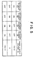
- phase-U output voltage V U of the three-phase three-level inverter shown in Fig. 1 has three levels E d /2, 0, and -E d /2 according to the on/off states of the switching elements 4A to 5B of the first and second switching element pairs, as shown in Fig. 5.
- each of the phase-V output voltage V V and a phase-W output voltage V W has three levels.
- phase-U output voltage V U shown in Fig. 2 can be obtained through the output terminal 16 by applying the gate signals S 4AG to S 5BG shown in Fig. 2 to the switching elements 4A to 5B, respectively.
- phase-V and phase-W gate signals (not shown) S 6AG to S 9BG are formed to obtain the phase-V output voltage V V and the phase-W output voltage V W through the output terminals 17 and 18.
- the difference between the phase-U output voltage V U and the phase-V output voltage V V is taken as the line U-V voltage V UV .
- the pulse width of the gate signals S 4AG to S 5BG is changed according to the percentage modulation m
- the line voltage obtained in the one-pulse mode can be changed by changing the percentage modulation m . That is, pulse width modulation is possible in the one-pulse mode.
- Fig. 3 is a diagram of a pulse mode corresponding to the three-pulse mode in the conventional method.
- S Ua designates a sinusoidal modulating wave
- S Ca designates a triangular carrier wave.
- the gate signals S 4AG to S 5BG are formed by comparison between the sinusoidal modulating wave S Ua and the triangular carrier wave S Ca .
- the percentage modulation corresponds to the amplitude of the sinusoidal modulating wave S Ua .
- the switching elements 4A to 5B are driven by the gate signals S 4AG to S 5BG to obtain the phase-U output voltage V U shown in Fig. 3.
- the phase-V and phase-W gate signals (not shown) S 6AG to S 9BG are formed to obtain the phase-V output voltage V V and the phase-W output voltage V W .
- the difference between the phase-in output voltage V U and the phase-V output voltage V V is taken as the line U-V voltage V UV .
- the line voltage can be controlled by pulse width modulation in each of the three-pulse mode and the one-pulse mode. It is therefore possible to avoid occurrence of a discontinuity of the line voltage, such as that occurring in the conventional inverter, at the time of transition from the three-pulse mode to the one-pulse mode at an inverter frequency f2 and, hence, to continuously change the line voltage.
- f3 designates the inverter frequency at which the line voltage corresponds to the maximum percentage modulation m max determined by the minimum switching element off time.
- the inverter In the range of inverter frequencies equal to or higher than f3, the inverter is operated by fixing the percentage modulation to the maximum percentage modulation m max .
- the proportion of the fundamental wave component of the line voltage is about 99 % of that attained by the conventional method in the one-pulse mode, if the minimum off time is about 200 ⁇ s and the maximum inverter frequency is about 200 Hz. That is, the line voltage can be controlled so as to be continuously changed without reducing the voltage utilization coefficient.
- Fig. 6 shows another three-phase three-level inverter having a different configuration.
- This inverter is constructed in such a manner that, in the inverter shown in Fig. 1, a capacitor 3 is connected between the reactor 2 and the minus terminal of the DC power source 1 instead of the capacitors 3A and 3B, a capacitor 3C is connected between the middle point of the first pair of switching elements 4A-4B and the middle point of the second pair of switching elements 5A-5B instead of the diodes 19 and 20, a capacitor 3D is connected between the middle point of the third pair of switching elements 6A-6B and the middle point of the fourth pair of switching elements 7A-7B instead of the diodes 21 and 22, and a capacitor 3E is connected between the middle point of the fifth pair of switching elements 8A-8B and the middle point of the sixth pair of switching elements 9A-9B instead of the diodes 23 and 24.
- phase-U output voltage V U of the inverter shown in Fig. 6 has three levels E d /2, 0, and -E d /2 according to the on/off states of the switching elements 4A to 5B of the first and second switching element pairs, as shown in Fig. 9.
- each of the phase-V output voltage V V and a phase-W output voltage V W has three levels.
- the line voltage can therefore be controlled by pulse width modulation in each of the three-pulse mode and the one-pulse mode, as in the case of the first embodiment.
- Figs. 7 and 8 respectively show the relationship between the gate signals S 4AG to S 5BG , the phase-in output voltage V U , the phase-V output voltage V V , and the line U-V voltage V UV in the one-pulse mode and the corresponding relationship in the three-pulse mode. That is, it is also possible to avoid occurrence of a discontinuity at the time of transition from the three-pulse mode to the one-pulse mode and to continuously change the line voltage as shown in Fig. 4 by using the inverter shown in Fig. 6.
- a three-phase three-level inverter is used as a main circuit and the on/off control of the inverter switching elements is effected in the above-described manner, thereby enabling the line voltage to be continuously changed to the maximum value as well as preventing an abrupt change in torque ripples or undesirable oscillation of the DC filter voltage, which cannot be avoided by the conventional method. It is also possible to reduce the change in the voltage at the time of switching of each switching element to half of the corresponding change in the conventional method, i.e., to E d /2 and therefore to realize an inverter unit improved in resistance to noise.
Landscapes
- Engineering & Computer Science (AREA)
- Power Engineering (AREA)
- Inverter Devices (AREA)
Applications Claiming Priority (2)
| Application Number | Priority Date | Filing Date | Title |
|---|---|---|---|
| JP301934/89 | 1989-11-22 | ||
| JP1301934A JP2566021B2 (ja) | 1989-11-22 | 1989-11-22 | インバータ装置の運転方法 |
Publications (3)
| Publication Number | Publication Date |
|---|---|
| EP0430044A2 true EP0430044A2 (de) | 1991-06-05 |
| EP0430044A3 EP0430044A3 (en) | 1991-10-16 |
| EP0430044B1 EP0430044B1 (de) | 1994-04-20 |
Family
ID=17902869
Family Applications (1)
| Application Number | Title | Priority Date | Filing Date |
|---|---|---|---|
| EP90122213A Revoked EP0430044B1 (de) | 1989-11-22 | 1990-11-20 | Verfahren zur Steuerung eines Wechselrichters |
Country Status (5)
| Country | Link |
|---|---|
| US (1) | US5155675A (de) |
| EP (1) | EP0430044B1 (de) |
| JP (1) | JP2566021B2 (de) |
| DE (1) | DE69008315T2 (de) |
| ES (1) | ES2051437T3 (de) |
Cited By (6)
| Publication number | Priority date | Publication date | Assignee | Title |
|---|---|---|---|---|
| AU667014B2 (en) * | 1993-09-01 | 1996-02-29 | Hitachi Limited | Three level power converting apparatus having means for balancing DC component thereof |
| WO2002013364A1 (en) * | 2000-08-10 | 2002-02-14 | Abb Ab | A method and a device for providing a vsc-converter with voltage |
| WO2002097960A1 (en) * | 2001-05-30 | 2002-12-05 | Abb Ab | A converter apparatus and a method for control thereof |
| US6522561B1 (en) | 1998-09-24 | 2003-02-18 | Aloys Wobben | Inverter for injecting sinusoidal currents into an alternating current network using positive and negative half wave circuits |
| WO2015027693A1 (zh) * | 2013-08-30 | 2015-03-05 | 华为技术有限公司 | 功率变换电路和功率变换系统 |
| CN104660078A (zh) * | 2015-01-15 | 2015-05-27 | 燕山大学 | 一种三相Cuk升降压型三电平逆变器 |
Families Citing this family (37)
| Publication number | Priority date | Publication date | Assignee | Title |
|---|---|---|---|---|
| US5731970A (en) * | 1989-12-22 | 1998-03-24 | Hitachi, Ltd. | Power conversion device and semiconductor module suitable for use in the device |
| JP2664275B2 (ja) * | 1990-09-14 | 1997-10-15 | 株式会社日立製作所 | 電力変換装置 |
| EP0838855B1 (de) * | 1991-09-20 | 2004-11-24 | Hitachi, Ltd. | Halbleitermodul |
| JP2765315B2 (ja) * | 1991-11-18 | 1998-06-11 | 株式会社日立製作所 | 電力変換装置及びこれを利用した電気車の制御装置 |
| US5517401A (en) * | 1992-02-07 | 1996-05-14 | Fuji Electric Co., Ltd. | Three level pulse width modulated inverter for an electric vehicle |
| JP3178075B2 (ja) * | 1992-04-23 | 2001-06-18 | 株式会社日立製作所 | 電力変換器の制御装置および電気車の制御装置 |
| AU651034B2 (en) * | 1992-04-24 | 1994-07-07 | Hitachi Limited | Power converter for converting DC voltage into AC phase voltage having three levels of positive, zero and negative voltage |
| JP2814837B2 (ja) * | 1992-06-04 | 1998-10-27 | 株式会社日立製作所 | 電力変換装置 |
| US5508218A (en) * | 1993-12-28 | 1996-04-16 | Lg Semicon Co., Ltd. | Method for fabricating a semiconductor memory |
| JP3153408B2 (ja) * | 1994-03-10 | 2001-04-09 | 株式会社日立製作所 | 直列多重電力変換器 |
| JPH08289561A (ja) * | 1995-02-14 | 1996-11-01 | Toshiba Corp | 電力変換装置 |
| US5592371A (en) * | 1995-05-17 | 1997-01-07 | General Motors Corporation | DC link inverter |
| US5594634A (en) * | 1995-05-17 | 1997-01-14 | General Motors Corporation | DC link inverter having soft-switched auxiliary devices |
| JP3262495B2 (ja) * | 1996-06-03 | 2002-03-04 | 株式会社東芝 | マルチレベルインバータ |
| US6058031A (en) * | 1997-10-23 | 2000-05-02 | General Electric Company | Five level high power motor drive converter and control system |
| JP3383588B2 (ja) * | 1998-08-04 | 2003-03-04 | 株式会社東芝 | 電力変換装置 |
| DE19961382A1 (de) * | 1999-07-31 | 2001-02-01 | Alstom Anlagen Und Antriebssys | Elektrische Schaltung, insbesondere für einen Mittelspannungsstromrichter |
| US6534949B2 (en) | 2001-03-29 | 2003-03-18 | General Electric Company | Motor drive converter and method with neutral point drift compensation |
| US20060049813A1 (en) * | 2003-01-14 | 2006-03-09 | Hendrix Machiel Antonius M | Three-Level dc-ac converter |
| US6842354B1 (en) * | 2003-08-08 | 2005-01-11 | Rockwell Automation Technologies, Inc. | Capacitor charge balancing technique for a three-level PWM power converter |
| US7219673B2 (en) * | 2004-08-25 | 2007-05-22 | Curtiss-Wright Electro-Mechanical Corporation | Transformerless multi-level power converter |
| JP5050395B2 (ja) * | 2006-04-24 | 2012-10-17 | 日産自動車株式会社 | 電力制御装置及び電力制御方法 |
| JP4811102B2 (ja) * | 2006-04-26 | 2011-11-09 | 日産自動車株式会社 | 電力変換装置の制御装置および制御方法 |
| JP5239235B2 (ja) * | 2006-10-13 | 2013-07-17 | 日産自動車株式会社 | 電力変換装置および電力変換方法 |
| US7782005B2 (en) * | 2006-11-07 | 2010-08-24 | Nissan Motor Co., Ltd. | Power converter control |
| DE102007013462B4 (de) | 2007-03-21 | 2018-08-09 | Renk Ag | Leistungselektronische Schaltungsanordnung für eine Drehfeldmaschine |
| EP2160828B1 (de) * | 2007-06-01 | 2016-05-04 | DRS Power & Control Technologies, Inc. | Vierpolneutralpunktgeklemmter dreiphasenumrichter mit nullgleichtaktspannungsausgang |
| US7986535B2 (en) * | 2007-07-17 | 2011-07-26 | Raytheon Company | Methods and apparatus for a cascade converter using series resonant cells with zero voltage switching |
| US7839023B2 (en) * | 2007-07-18 | 2010-11-23 | Raytheon Company | Methods and apparatus for three-phase inverter with reduced energy storage |
| JP5072097B2 (ja) * | 2008-01-21 | 2012-11-14 | 学校法人東京電機大学 | 3相電圧形インバータシステム |
| CN102223091A (zh) * | 2010-04-14 | 2011-10-19 | 艾默生网络能源系统北美公司 | 一种ac/dc变换器 |
| WO2012040257A1 (en) * | 2010-09-21 | 2012-03-29 | Curtiss-Wright Electro-Mechanical Corporation | Two terminal multilevel converter |
| EP2779345B8 (de) * | 2013-03-14 | 2015-06-10 | ABB Technology Oy | Verfahren zum Steuern des Schaltzweigs eines dreistufigen aktiven Neutralpunktklemmenumrichters und Schaltzweig hierfür |
| WO2014174597A1 (ja) | 2013-04-23 | 2014-10-30 | 三菱電機株式会社 | 交流電動機の制御装置 |
| US9647575B2 (en) | 2013-04-23 | 2017-05-09 | Mitsubishi Electric Corporation | Power converter |
| CN103973152B (zh) * | 2014-04-04 | 2016-10-05 | 深圳职业技术学院 | 一种脉冲宽度调制控制方法及装置 |
| CN106533236B (zh) * | 2016-12-15 | 2018-10-16 | 电子科技大学 | 一种三电平逆变器的最小开关损耗实现方法 |
Family Cites Families (5)
| Publication number | Priority date | Publication date | Assignee | Title |
|---|---|---|---|---|
| US3870945A (en) * | 1974-02-28 | 1975-03-11 | Gen Electric | Inverter system having smooth switching between operational modes |
| CA1143787A (en) * | 1978-09-21 | 1983-03-29 | Exxon Research And Engineering Company | Bridge converter circuit |
| US4203151A (en) * | 1978-09-21 | 1980-05-13 | Exxon Research & Engineering Co. | High-voltage converter circuit |
| JPS56121369A (en) * | 1980-02-25 | 1981-09-24 | Toshiba Corp | Inverter control circuit |
| ES2046287T3 (es) * | 1988-04-05 | 1994-02-01 | S.A. Acec Transport | Procedimiento de modulacion multinivel en amplitud de impulsion y modulador que aplica este procedimiento. |
-
1989
- 1989-11-22 JP JP1301934A patent/JP2566021B2/ja not_active Expired - Lifetime
-
1990
- 1990-10-30 US US07/605,486 patent/US5155675A/en not_active Expired - Lifetime
- 1990-11-20 DE DE69008315T patent/DE69008315T2/de not_active Revoked
- 1990-11-20 EP EP90122213A patent/EP0430044B1/de not_active Revoked
- 1990-11-20 ES ES90122213T patent/ES2051437T3/es not_active Expired - Lifetime
Cited By (8)
| Publication number | Priority date | Publication date | Assignee | Title |
|---|---|---|---|---|
| AU667014B2 (en) * | 1993-09-01 | 1996-02-29 | Hitachi Limited | Three level power converting apparatus having means for balancing DC component thereof |
| US6522561B1 (en) | 1998-09-24 | 2003-02-18 | Aloys Wobben | Inverter for injecting sinusoidal currents into an alternating current network using positive and negative half wave circuits |
| WO2002013364A1 (en) * | 2000-08-10 | 2002-02-14 | Abb Ab | A method and a device for providing a vsc-converter with voltage |
| WO2002097960A1 (en) * | 2001-05-30 | 2002-12-05 | Abb Ab | A converter apparatus and a method for control thereof |
| WO2015027693A1 (zh) * | 2013-08-30 | 2015-03-05 | 华为技术有限公司 | 功率变换电路和功率变换系统 |
| US9787217B2 (en) | 2013-08-30 | 2017-10-10 | Huawei Technologies Co., Ltd. | Power conversion circuit and power conversion system |
| CN104660078A (zh) * | 2015-01-15 | 2015-05-27 | 燕山大学 | 一种三相Cuk升降压型三电平逆变器 |
| CN104660078B (zh) * | 2015-01-15 | 2017-04-12 | 燕山大学 | 一种三相Cuk升降压型三电平逆变器 |
Also Published As
| Publication number | Publication date |
|---|---|
| US5155675A (en) | 1992-10-13 |
| ES2051437T3 (es) | 1994-06-16 |
| EP0430044B1 (de) | 1994-04-20 |
| JPH03164070A (ja) | 1991-07-16 |
| DE69008315T2 (de) | 1994-08-04 |
| DE69008315D1 (de) | 1994-05-26 |
| EP0430044A3 (en) | 1991-10-16 |
| JP2566021B2 (ja) | 1996-12-25 |
Similar Documents
| Publication | Publication Date | Title |
|---|---|---|
| US5155675A (en) | Method of controlling an inverter | |
| US4691269A (en) | PWM inverter apparatus | |
| EP0697763B1 (de) | Mehrfach gekoppelter leistungswandler und seine steuerverfahren | |
| JP2577738B2 (ja) | Pwmインバ−タ装置 | |
| US4599685A (en) | Control circuit for power converter apparatus | |
| US4295189A (en) | Apparatus and method for generating waveforms which are particularly suitable for a PWM-driven motor | |
| KR920017340A (ko) | 교류 모터 구동 시스템 | |
| US5747958A (en) | Circuit arrangement for powering a two-phase asynchronous motor | |
| JPH04236171A (ja) | インバータの出力電圧波形歪み抑制法 | |
| JPS6036711B2 (ja) | インバ−タ装置 | |
| JP2021044993A (ja) | 3レベル電力変換器の制御装置 | |
| JP4277360B2 (ja) | 3レベルインバータの制御装置 | |
| JPH1052062A (ja) | 3レベルインバータの制御装置 | |
| JPH09149658A (ja) | 直列多重型インバータ装置 | |
| JP3251805B2 (ja) | Npcインバータ装置及びその制御方法 | |
| JP3316448B2 (ja) | 半導体電力変換装置 | |
| JP3116714B2 (ja) | 3レベルインバータの制御方法 | |
| JPH0775346A (ja) | Pwmインバータ装置 | |
| JPH0421363A (ja) | インバータ装置 | |
| JPH0447553B2 (de) | ||
| JPH01186172A (ja) | パルス幅変調形インバータ制御装置 | |
| JPS60229676A (ja) | Pwmインバ−タ | |
| JPH0156636B2 (de) | ||
| JPH0437670B2 (de) | ||
| JPS62185573A (ja) | ブリツジ型インバ−タの制御方式 |
Legal Events
| Date | Code | Title | Description |
|---|---|---|---|
| PUAI | Public reference made under article 153(3) epc to a published international application that has entered the european phase |
Free format text: ORIGINAL CODE: 0009012 |
|
| AK | Designated contracting states |
Kind code of ref document: A2 Designated state(s): CH DE ES LI SE |
|
| PUAL | Search report despatched |
Free format text: ORIGINAL CODE: 0009013 |
|
| AK | Designated contracting states |
Kind code of ref document: A3 Designated state(s): CH DE ES LI SE |
|
| 17P | Request for examination filed |
Effective date: 19920320 |
|
| 17Q | First examination report despatched |
Effective date: 19930706 |
|
| GRAA | (expected) grant |
Free format text: ORIGINAL CODE: 0009210 |
|
| AK | Designated contracting states |
Kind code of ref document: B1 Designated state(s): CH DE ES LI SE |
|
| REF | Corresponds to: |
Ref document number: 69008315 Country of ref document: DE Date of ref document: 19940526 |
|
| REG | Reference to a national code |
Ref country code: ES Ref legal event code: FG2A Ref document number: 2051437 Country of ref document: ES Kind code of ref document: T3 |
|
| PLBI | Opposition filed |
Free format text: ORIGINAL CODE: 0009260 |
|
| PLBI | Opposition filed |
Free format text: ORIGINAL CODE: 0009260 |
|
| EAL | Se: european patent in force in sweden |
Ref document number: 90122213.3 |
|
| 26 | Opposition filed |
Opponent name: ABB MANAGEMENT AG, BADEN TEI/IMMATERIALGUETERRECHT Effective date: 19941228 |
|
| 26 | Opposition filed |
Opponent name: ABB PATENT GMBH Effective date: 19950113 Opponent name: ABB MANAGEMENT AG, BADEN TEI/IMMATERIALGUETERRECHT Effective date: 19941228 |
|
| PGFP | Annual fee paid to national office [announced via postgrant information from national office to epo] |
Ref country code: SE Payment date: 19961118 Year of fee payment: 7 |
|
| PGFP | Annual fee paid to national office [announced via postgrant information from national office to epo] |
Ref country code: ES Payment date: 19961129 Year of fee payment: 7 |
|
| PGFP | Annual fee paid to national office [announced via postgrant information from national office to epo] |
Ref country code: DE Payment date: 19961202 Year of fee payment: 7 |
|
| PGFP | Annual fee paid to national office [announced via postgrant information from national office to epo] |
Ref country code: CH Payment date: 19961206 Year of fee payment: 7 |
|
| RDAH | Patent revoked |
Free format text: ORIGINAL CODE: EPIDOS REVO |
|
| RDAG | Patent revoked |
Free format text: ORIGINAL CODE: 0009271 |
|
| STAA | Information on the status of an ep patent application or granted ep patent |
Free format text: STATUS: PATENT REVOKED |
|
| REG | Reference to a national code |
Ref country code: CH Ref legal event code: PL |
|
| 27W | Patent revoked |
Effective date: 19961205 |
|
| PLAB | Opposition data, opponent's data or that of the opponent's representative modified |
Free format text: ORIGINAL CODE: 0009299OPPO |
|
| R26 | Opposition filed (corrected) |
Opponent name: ABB MANAGEMENT AG, BADEN TEI/IMMATERIALGUETERRECHT Effective date: 19941228 |