EP0430429A2 - Verfahren zur Herstellung einer Halbleiteranordnung - Google Patents
Verfahren zur Herstellung einer Halbleiteranordnung Download PDFInfo
- Publication number
- EP0430429A2 EP0430429A2 EP90311670A EP90311670A EP0430429A2 EP 0430429 A2 EP0430429 A2 EP 0430429A2 EP 90311670 A EP90311670 A EP 90311670A EP 90311670 A EP90311670 A EP 90311670A EP 0430429 A2 EP0430429 A2 EP 0430429A2
- Authority
- EP
- European Patent Office
- Prior art keywords
- layer
- providing
- polysilicon
- oxide
- layers
- Prior art date
- Legal status (The legal status is an assumption and is not a legal conclusion. Google has not performed a legal analysis and makes no representation as to the accuracy of the status listed.)
- Ceased
Links
Images


Classifications
-
- H—ELECTRICITY
- H10—SEMICONDUCTOR DEVICES; ELECTRIC SOLID-STATE DEVICES NOT OTHERWISE PROVIDED FOR
- H10D—INORGANIC ELECTRIC SEMICONDUCTOR DEVICES
- H10D30/00—Field-effect transistors [FET]
- H10D30/01—Manufacture or treatment
- H10D30/021—Manufacture or treatment of FETs having insulated gates [IGFET]
- H10D30/0411—Manufacture or treatment of FETs having insulated gates [IGFET] of FETs having floating gates
-
- H—ELECTRICITY
- H10—SEMICONDUCTOR DEVICES; ELECTRIC SOLID-STATE DEVICES NOT OTHERWISE PROVIDED FOR
- H10D—INORGANIC ELECTRIC SEMICONDUCTOR DEVICES
- H10D64/00—Electrodes of devices having potential barriers
- H10D64/01—Manufacture or treatment
- H10D64/031—Manufacture or treatment of data-storage electrodes
- H10D64/035—Manufacture or treatment of data-storage electrodes comprising conductor-insulator-conductor-insulator-semiconductor structures
Definitions
- the present invention relates to processes for fabricating semiconductor devices; For example, processes for fabricating control gate lines for floating gate field effect transistors.
- the gate structure of a conventional floating gate field effect transistor includes a gate oxide layer provided on a substrate, a floating gate provided on the gate oxide layer, and a control gate separated from the floating gate by an inter-gate oxide layer.
- the control gate has conventionally been formed of a polysilicon layer or a polysilicon layer with a silicide layer overlying the polysilicon layer.
- the control gate is usually fabricated with a polysilicon layer adjacent to the inter-gate oxide in order to maintain the device characteristics provided by a polysilicon gate.
- a further problem associated with the formation of a multi-layer control gate is that the device must be removed from the furnace tube, or vacuum chamber, after the deposition of the polysilicon layer to allow the polysilicon layer to be doped before the silicide layer is deposited.
- the device Each time the device is removed from the furnace tube one of two problems arise.
- the cooling of the furnace tube to insert the wafers causes the polysilicon accumulated on the tube walls to warp or break the furnace tube due to the divergent coefficients of thermal expansion of polysilicon and quartz.
- the tube is maintained at a high temperature and the wafers are inserted into a hot tube there is a high risk of wafer oxidation, even if a flow of an inert gas is provided, which causes yield problems.
- Buried contacts require the removal of the inter-gate oxide and the gate oxide in the region where the buried contact is to be formed. This leaves the substrate exposed and oxidation of the substrate in the buried contact region as the wafer is inserted into a hot furnace tube will ruin a die.
- the present invention provides a process for fabricating a floating gate field-effect transistor comprises the steps of (a) providing a gate oxide on the substrate, (b) providing a floating gate line on the gate oxide, (c) providing an intergate oxide layer overlying the gate oxide and the floating gate line, (d) providing control gate layers, including a first undoped polysilicon layer overlying the intergate oxide layer, a silicide layer overlying the first polysilicon layer, and a second undoped polysilicon layer overlying the silicide layer, (e) annealing the control gate layers in an environment including POCl3, (f) etching the control gate layers to form a control gate line, (g) etching the floating gate line using the control gate line as a mask to form a floating gate, and (h) implanting source and drain regions using the control gate line as a mask.
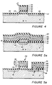
- Figs. 1-4 are cross-sectional views useful for describing the process of the present invention.
- Fig. 5A is a cross-sectional view along line 5A-5A in Fig. 6 useful in describing the process of the present invention
- Fig. 5B is a cross-sectional view along line 5B-5B in Fig.6 useful in describing an alternative embodiment of the process of the present invention
- Fig. 6 is a simplified plan view of a semiconductor device fabricated in accordance with the process of the present invention.
- Fig. 7 is a simplified plan view useful in describing the process of the present invention.
- the present invention will be described with reference to Figs. 1-7.
- the process of the present invention is particularly useful and is described below in the fabrication of floating gate field effect transistors.
- the process of the present invention is also applicable to the formation of any conductive line for a semiconductor device in either a bipolar or an MOS process.
- the process of the present invention may be used to fabricate gate structures for non-floating gate field effect transistors or conductive lines for bipolar devices.
- the process of the present invention begins with a substrate 10 which is thermally oxidized to form a gate oxide 12.
- the gate oxide 12 may be a deposited oxide; however, thermal oxides are considered to be higher-quality oxides more suitable for use as a gate oxide.
- field oxide regions are provided to define the active regions where individual field effect transistors would be formed.
- a floating gate material layer 14 is provided over gate oxide 12.
- floating gate material layer 14 is formed of polysilicon.
- the floating gate material layer 14 may have a thickness ranging from approximately 1,000 to 3,000 ⁇ , and is approximately 1,500 ⁇ in the preferred embodiment.
- the floating gate material layer 14 is then doped by annealing the device in an atmosphere comprising phosphorous oxychloride (POCl3) . This anneal is conducted for a time sufficient to provide floating gate material layer 14 with a doping concentration of approximately 1x1020cm - 3. In the preferred embodiment, the POCl3 concentration is approximately 0.1%, and the device is annealed at a temperature of approximately 875°C for approximately fifteen (15) minutes. Thereafter, floating gate material layer 14 is etched to form floating gate lines 14 as shown in the simplified plan view of Fig. 7.
- intergate oxide layer 16 is provided over gate oxide 12 and floating gate lines 14.
- intergate oxide layer 16 is a 200 ⁇ thermal oxide grown by annealing the device at approximately 1100°C for approximately ten minutes in an environment including dry oxygen and HCl.
- intergate oxide 16 may be a deposited oxide.
- Polysilicon layer 18 is formed as an undoped layer using conventional deposition techniques.
- a silicide layer 20 is provided on polysilicon layer 18.
- the silicide may be selected from the group including TaSi2 , WSi2 , TiSi2, and MoSi2 ; WSi2 , the preferred silicide, is deposited, for example, in an environment including SiH2Cl2 and WF6 at a temperature of approximately 600°C.
- the thickness of silicide layer 20 may range from approximately 500 to 5,000 ⁇ ; in the preferred embodiment silicide layer 20 is a thickness of approximately 2,000 ⁇ .
- An undoped polysilicon layer 22 is then provided over silicide layer 20.
- the thickness of polysilicon layer 22 may be approximately 50 to 2,500 ⁇ , with the preferred embodiment having a thickness of approximately 1,000 ⁇ .
- Polysilicon layers 18 and 22 are formed as undoped polysilicon in order to improve the adhesion of these layers to silicide layer 20.
- polysilicon layers 18 and 22 are doped by annealing the device in a POCl3 environment.
- the desired impurity concentration (doping level) in polysilicon layers 18 and 22 is greater than approximately 5x1019cm - 3 and in the preferred embodiment the doping level is approximately 3-5x1020cm - 3.
- polysilicon layers 18 and 22 are doped in an environment including a nitrogen carrier, approximately 0.1% POCl3 , and approximately 5% oxygen.
- the anneal is performed at approximately 875°C for approximately thirty (30) minutes.
- the doping of polysilicon layer 18 is not adversely affected by the presence of silicide layer 20.
- polysilicon layer 18, silicide layer 20, and polysilicon layer 22 using a single pump-down cycle because the device is not required to be removed from the vacuum chamber used to deposit these layers in order to dope the individual layers as they are formed.
- capping oxide layer 24 is a thermal oxide having a thickness of approximately 1,000 ⁇ , formed by oxidation in an atmosphere including dry oxygen and HCl at a temperature of approximately 900°C for a period of approximately fifty (50) minutes.
- control gate layers, 18, 20, 22 and oxide layer 24 The etching of the control gate layers, 18, 20, 22 and oxide layer 24 to form control gate lines will be described with reference to Fig. 3.
- a photo-resist layer (not shown) is formed on oxide layer 24, and is then patterned using a conventional lift-off process so that the photo-resist remains on the portions of the control gate layers and oxide layer 24 which will form control gate lines.
- oxide layer 24 is etched using an etchant which is effective for silicon oxide, and subsequently polysilicon layer 18, silicide layer 20, and polysilicon layer 22 are etched using an etchant which is effective for etching polysilicon. Because etchants which are effective for etching polysilicon are generally not selective for silicon oxide, intergate oxide layer 16 serves as an etch-stop layer.
- This etching process forms control gate lines 26 (Fig. 6).
- the relationship of a floating gate line 14 and a control gate line 26 is shown in the plan view of Fig. 7.
- the sectional view of Fig. 3 is in the direction of arrow A in Fig. 7.
- intergate oxide layer 16 is etched using the control gate line 26 as a mask, and then the portions of floating gate lines 14 which do not underlie control gate line 26 are removed by etching; the portions of the floating gate line which are removed by etching are designated 151 and 152 in Fig. 7.
- the etching of floating gate line 14 to form a floating gate 114 completes the fabrication of gate structure 28.
- Fig. 5A which corresponds to a view in the direction of arrow B in Fig. 7, shows floating gate 114 under inter-gate oxide 16 and control gate line 26 (including layers 18, 20, and 22). Gate structure 28 is then used as a mask to implant self-aligned source and drain regions 36, 38.
- the source/drain implant is driven and a thick thermal oxide (not shown) is grown on the sides of gate structure 28 to electrically insulate the floating gates 114.
- a thick thermal oxide (not shown) is grown on the sides of gate structure 28 to electrically insulate the floating gates 114.
- the fabrication of the field-effect transistor is completed by providing metallization and passivation layers in accordance with conventional techniques.
- FIG. 6 one example of a buried contact is an extension 27 of control gate line 262 which contacts the drain region 381 of a field effect transistor formed on adjacent control gate line 261.
- FIG. 5B A simplified cross-sectional view of a floating gate field effect transistor having a buried contact is shown in the cross-sectional view of Fig. 5B, taken along line 5B-5B in Fig. 6.
- a portion of intergate oxide 16 and gate oxide 12 are removed by etching prior to the formation of the control gate material layers.
- This etching is performed by providing a photo-resist layer, which is patterned using conventional lift-off techniques so that only the buried contact regions are exposed. Polysilicon layer 18, silicide layer 20, and polysilicon layer 22 are then formed in accordance with the process described above.
- the use of a load lock chamber is particularly useful for providing the control gate layers when buried contacts are formed so that oxidation of the substrate in the region of buried contact 40 is prevented.
Landscapes
- Semiconductor Memories (AREA)
- Non-Volatile Memory (AREA)
- Electrodes Of Semiconductors (AREA)
- Internal Circuitry In Semiconductor Integrated Circuit Devices (AREA)
Applications Claiming Priority (2)
| Application Number | Priority Date | Filing Date | Title |
|---|---|---|---|
| US07/442,903 US4992391A (en) | 1989-11-29 | 1989-11-29 | Process for fabricating a control gate for a floating gate FET |
| US442903 | 1989-11-29 |
Publications (2)
| Publication Number | Publication Date |
|---|---|
| EP0430429A2 true EP0430429A2 (de) | 1991-06-05 |
| EP0430429A3 EP0430429A3 (en) | 1991-10-16 |
Family
ID=23758615
Family Applications (1)
| Application Number | Title | Priority Date | Filing Date |
|---|---|---|---|
| EP19900311670 Ceased EP0430429A3 (en) | 1989-11-29 | 1990-10-24 | A process for fabricating a semiconductor device |
Country Status (3)
| Country | Link |
|---|---|
| US (1) | US4992391A (de) |
| EP (1) | EP0430429A3 (de) |
| JP (1) | JPH03173480A (de) |
Cited By (1)
| Publication number | Priority date | Publication date | Assignee | Title |
|---|---|---|---|---|
| EP0860863A3 (de) * | 1997-02-25 | 1998-10-21 | Tokyo Electron Limited | Schichtstruktur aus Polysilizium und Wolframsilizid und Herstellungsverfahren dafür |
Families Citing this family (56)
| Publication number | Priority date | Publication date | Assignee | Title |
|---|---|---|---|---|
| KR920010062B1 (ko) * | 1989-04-03 | 1992-11-13 | 현대전자산업 주식회사 | 반도체 장치의 실리사이드 형성방법 |
| US5629218A (en) * | 1989-12-19 | 1997-05-13 | Texas Instruments Incorporated | Method for forming a field-effect transistor including a mask body and source/drain contacts |
| KR970009976B1 (ko) * | 1991-08-26 | 1997-06-19 | 아메리칸 텔리폰 앤드 텔레그라프 캄파니 | 증착된 반도체상에 형성된 개선된 유전체 |
| US5208170A (en) * | 1991-09-18 | 1993-05-04 | International Business Machines Corporation | Method for fabricating bipolar and CMOS devices in integrated circuits using contact metallization for local interconnect and via landing |
| US5284786A (en) * | 1992-08-14 | 1994-02-08 | National Semiconductor Corporation | Method of making a split floating gate EEPROM cell |
| EP0746027A3 (de) * | 1995-05-03 | 1998-04-01 | Applied Materials, Inc. | Auf einer integrierten Schaltung hergestellter Polysilizium/Wolframsilizid-Mehrschichtverbund und verbessertes Herstellungsverfahren |
| JP3383140B2 (ja) | 1995-10-02 | 2003-03-04 | 株式会社東芝 | 不揮発性半導体記憶装置の製造方法 |
| US5654219A (en) * | 1996-02-07 | 1997-08-05 | Texas Instruments Incorporated | Annealed poly-silicide etch process |
| IT1289540B1 (it) * | 1996-07-10 | 1998-10-15 | Sgs Thomson Microelectronics | Metodo per trasformare automaticamente la fabbricazione di una cella di memoria eprom nella fabbricazione di una cella di memoria |
| KR19980032827A (ko) * | 1996-10-08 | 1998-07-25 | 윌리엄비.켐플러 | 트랜지스터 상호접속 구조 및 그 방법 |
| US5840607A (en) * | 1996-10-11 | 1998-11-24 | Taiwan Semiconductor Manufacturing Company, Ltd. | Method of forming undoped/in-situ doped/undoped polysilicon sandwich for floating gate application |
| US6060360A (en) * | 1997-04-14 | 2000-05-09 | Taiwan Semiconductor Manufacturing Company | Method of manufacture of P-channel EEprom and flash EEprom devices |
| US6768165B1 (en) * | 1997-08-01 | 2004-07-27 | Saifun Semiconductors Ltd. | Two bit non-volatile electrically erasable and programmable semiconductor memory cell utilizing asymmetrical charge trapping |
| US6376348B1 (en) * | 1997-09-30 | 2002-04-23 | Siemens Aktiengesellschaft | Reliable polycide gate stack with reduced sheet resistance and thickness |
| TW374801B (en) * | 1998-04-21 | 1999-11-21 | Promos Technologies Inc | Method of interface flattening of polycide/polysilicon/Wsix |
| US6048766A (en) * | 1998-10-14 | 2000-04-11 | Advanced Micro Devices | Flash memory device having high permittivity stacked dielectric and fabrication thereof |
| US6614692B2 (en) * | 2001-01-18 | 2003-09-02 | Saifun Semiconductors Ltd. | EEPROM array and method for operation thereof |
| US6584017B2 (en) | 2001-04-05 | 2003-06-24 | Saifun Semiconductors Ltd. | Method for programming a reference cell |
| US7098107B2 (en) * | 2001-11-19 | 2006-08-29 | Saifun Semiconductor Ltd. | Protective layer in memory device and method therefor |
| US6812515B2 (en) * | 2001-11-26 | 2004-11-02 | Hynix Semiconductor, Inc. | Polysilicon layers structure and method of forming same |
| US6700818B2 (en) * | 2002-01-31 | 2004-03-02 | Saifun Semiconductors Ltd. | Method for operating a memory device |
| US6917544B2 (en) * | 2002-07-10 | 2005-07-12 | Saifun Semiconductors Ltd. | Multiple use memory chip |
| US7136304B2 (en) | 2002-10-29 | 2006-11-14 | Saifun Semiconductor Ltd | Method, system and circuit for programming a non-volatile memory array |
| US7178004B2 (en) * | 2003-01-31 | 2007-02-13 | Yan Polansky | Memory array programming circuit and a method for using the circuit |
| US7142464B2 (en) | 2003-04-29 | 2006-11-28 | Saifun Semiconductors Ltd. | Apparatus and methods for multi-level sensing in a memory array |
| US7123532B2 (en) * | 2003-09-16 | 2006-10-17 | Saifun Semiconductors Ltd. | Operating array cells with matched reference cells |
| US7317633B2 (en) | 2004-07-06 | 2008-01-08 | Saifun Semiconductors Ltd | Protection of NROM devices from charge damage |
| US7095655B2 (en) * | 2004-08-12 | 2006-08-22 | Saifun Semiconductors Ltd. | Dynamic matching of signal path and reference path for sensing |
| US20060068551A1 (en) * | 2004-09-27 | 2006-03-30 | Saifun Semiconductors, Ltd. | Method for embedding NROM |
| US7638850B2 (en) * | 2004-10-14 | 2009-12-29 | Saifun Semiconductors Ltd. | Non-volatile memory structure and method of fabrication |
| US20060146624A1 (en) * | 2004-12-02 | 2006-07-06 | Saifun Semiconductors, Ltd. | Current folding sense amplifier |
| US7535765B2 (en) | 2004-12-09 | 2009-05-19 | Saifun Semiconductors Ltd. | Non-volatile memory device and method for reading cells |
| CN1838323A (zh) | 2005-01-19 | 2006-09-27 | 赛芬半导体有限公司 | 可预防固定模式编程的方法 |
| US8053812B2 (en) | 2005-03-17 | 2011-11-08 | Spansion Israel Ltd | Contact in planar NROM technology |
| US20070141788A1 (en) * | 2005-05-25 | 2007-06-21 | Ilan Bloom | Method for embedding non-volatile memory with logic circuitry |
| EP1746645A3 (de) | 2005-07-18 | 2009-01-21 | Saifun Semiconductors Ltd. | Speicherzellenanordnung mit sub-minimalem Wortleitungsabstand und Verfahren zu deren Herstellung |
| US7668017B2 (en) | 2005-08-17 | 2010-02-23 | Saifun Semiconductors Ltd. | Method of erasing non-volatile memory cells |
| US20070096199A1 (en) * | 2005-09-08 | 2007-05-03 | Eli Lusky | Method of manufacturing symmetric arrays |
| US7221138B2 (en) | 2005-09-27 | 2007-05-22 | Saifun Semiconductors Ltd | Method and apparatus for measuring charge pump output current |
| US20070087503A1 (en) * | 2005-10-17 | 2007-04-19 | Saifun Semiconductors, Ltd. | Improving NROM device characteristics using adjusted gate work function |
| US20070120180A1 (en) * | 2005-11-25 | 2007-05-31 | Boaz Eitan | Transition areas for dense memory arrays |
| US7352627B2 (en) * | 2006-01-03 | 2008-04-01 | Saifon Semiconductors Ltd. | Method, system, and circuit for operating a non-volatile memory array |
| US7808818B2 (en) * | 2006-01-12 | 2010-10-05 | Saifun Semiconductors Ltd. | Secondary injection for NROM |
| US20070173017A1 (en) * | 2006-01-20 | 2007-07-26 | Saifun Semiconductors, Ltd. | Advanced non-volatile memory array and method of fabrication thereof |
| US7760554B2 (en) * | 2006-02-21 | 2010-07-20 | Saifun Semiconductors Ltd. | NROM non-volatile memory and mode of operation |
| US8253452B2 (en) * | 2006-02-21 | 2012-08-28 | Spansion Israel Ltd | Circuit and method for powering up an integrated circuit and an integrated circuit utilizing same |
| US7692961B2 (en) * | 2006-02-21 | 2010-04-06 | Saifun Semiconductors Ltd. | Method, circuit and device for disturb-control of programming nonvolatile memory cells by hot-hole injection (HHI) and by channel hot-electron (CHE) injection |
| US7638835B2 (en) | 2006-02-28 | 2009-12-29 | Saifun Semiconductors Ltd. | Double density NROM with nitride strips (DDNS) |
| US7701779B2 (en) * | 2006-04-27 | 2010-04-20 | Sajfun Semiconductors Ltd. | Method for programming a reference cell |
| US7605579B2 (en) * | 2006-09-18 | 2009-10-20 | Saifun Semiconductors Ltd. | Measuring and controlling current consumption and output current of charge pumps |
| JP2008085131A (ja) * | 2006-09-28 | 2008-04-10 | Toshiba Corp | 半導体記憶装置 |
| JP2012038934A (ja) * | 2010-08-06 | 2012-02-23 | Toshiba Corp | 不揮発性半導体記憶装置とその製造方法 |
| US8890254B2 (en) | 2012-09-14 | 2014-11-18 | Macronix International Co., Ltd. | Airgap structure and method of manufacturing thereof |
| CN107924816B (zh) | 2015-06-26 | 2021-08-31 | 东京毅力科创株式会社 | 具有含硅减反射涂层或硅氧氮化物相对于不同膜或掩模的可控蚀刻选择性的气相蚀刻 |
| KR20180014207A (ko) | 2015-06-26 | 2018-02-07 | 도쿄엘렉트론가부시키가이샤 | 기상 식각 시스템 및 방법 |
| US20230395729A1 (en) * | 2020-12-10 | 2023-12-07 | Intel Corporation | Memory devices with gradient-doped control gate material |
Family Cites Families (11)
| Publication number | Priority date | Publication date | Assignee | Title |
|---|---|---|---|---|
| GB1399163A (en) * | 1972-11-08 | 1975-06-25 | Ferranti Ltd | Methods of manufacturing semiconductor devices |
| US4128670A (en) * | 1977-11-11 | 1978-12-05 | International Business Machines Corporation | Fabrication method for integrated circuits with polysilicon lines having low sheet resistance |
| GB2077993A (en) * | 1980-06-06 | 1981-12-23 | Standard Microsyst Smc | Low sheet resistivity composite conductor gate MOS device |
| NL186352C (nl) * | 1980-08-27 | 1990-11-01 | Philips Nv | Werkwijze ter vervaardiging van een halfgeleiderinrichting. |
| US4403394A (en) * | 1980-12-17 | 1983-09-13 | International Business Machines Corporation | Formation of bit lines for ram device |
| US4389257A (en) * | 1981-07-30 | 1983-06-21 | International Business Machines Corporation | Fabrication method for high conductivity, void-free polysilicon-silicide integrated circuit electrodes |
| IT1213120B (it) * | 1984-01-10 | 1989-12-14 | Ates Componenti Elettron | Processo per la fabbricazione di transistori mos complementari a basse tensioni di soglia in circuiti integrati ad alta densita' e struttura da esso risultante. |
| US4640844A (en) * | 1984-03-22 | 1987-02-03 | Siemens Aktiengesellschaft | Method for the manufacture of gate electrodes formed of double layers of metal silicides having a high melting point and doped polycrystalline silicon |
| EP0160965B1 (de) * | 1984-05-07 | 1990-01-31 | Kabushiki Kaisha Toshiba | Verfahren zum Herstellen einer Halbleiteranordnung mit einer Gateelektrodenstapel-Struktur |
| US4740479A (en) * | 1985-07-05 | 1988-04-26 | Siemens Aktiengesellschaft | Method for the manufacture of cross-couplings between n-channel and p-channel CMOS field effect transistors of static write-read memories |
| JP4512131B2 (ja) * | 2007-12-28 | 2010-07-28 | 株式会社日立製作所 | 放射線撮像装置、核医学診断装置及び位置調整装置 |
-
1989
- 1989-11-29 US US07/442,903 patent/US4992391A/en not_active Expired - Lifetime
-
1990
- 1990-10-24 EP EP19900311670 patent/EP0430429A3/en not_active Ceased
- 1990-11-29 JP JP2341158A patent/JPH03173480A/ja active Pending
Cited By (3)
| Publication number | Priority date | Publication date | Assignee | Title |
|---|---|---|---|---|
| EP0860863A3 (de) * | 1997-02-25 | 1998-10-21 | Tokyo Electron Limited | Schichtstruktur aus Polysilizium und Wolframsilizid und Herstellungsverfahren dafür |
| US6404021B1 (en) | 1997-02-25 | 2002-06-11 | Tokyo Electron Limited | Laminated structure and a method of forming the same |
| US6489208B2 (en) | 1997-02-25 | 2002-12-03 | Tokyo Electron Limited | Method of forming a laminated structure to enhance metal silicide adhesion on polycrystalline silicon |
Also Published As
| Publication number | Publication date |
|---|---|
| EP0430429A3 (en) | 1991-10-16 |
| US4992391A (en) | 1991-02-12 |
| JPH03173480A (ja) | 1991-07-26 |
Similar Documents
| Publication | Publication Date | Title |
|---|---|---|
| US4992391A (en) | Process for fabricating a control gate for a floating gate FET | |
| US4422885A (en) | Polysilicon-doped-first CMOS process | |
| US4078947A (en) | Method for forming a narrow channel length MOS field effect transistor | |
| US5065208A (en) | Integrated bipolar and CMOS transistor with titanium nitride interconnections | |
| JP2806477B2 (ja) | 浅いシリサイドの接合の製造方法 | |
| JP2848299B2 (ja) | 半導体装置及びその製造方法 | |
| KR900008207B1 (ko) | 반도체기억장치 | |
| US6136674A (en) | Mosfet with gate plug using differential oxide growth | |
| KR19980033385A (ko) | 측면 방향 게터링을 이용한 반도체 장치 제조 방법 | |
| KR0133540B1 (ko) | 섈로우 npn 에미터 및 mosfet 소오스/드레인을 형성하기 위한 bicmos 방법 | |
| EP0399231B1 (de) | Verfahren zur Herstellung eines Halbleiterbauteils | |
| EP0459398B1 (de) | Herstellungsverfahren eines Kanals in MOS-Halbleiteranordnung | |
| US4517731A (en) | Double polysilicon process for fabricating CMOS integrated circuits | |
| US4877748A (en) | Bipolar process for forming shallow NPN emitters | |
| US4553314A (en) | Method for making a semiconductor device | |
| US5115296A (en) | Preferential oxidization self-aligned contact technology | |
| EP0023528A1 (de) | Doppelt diffundierte Transistor-Struktur und Verfahren zu deren Herstellung | |
| US4350991A (en) | Narrow channel length MOS field effect transistor with field protection region for reduced source-to-substrate capacitance | |
| JP2823819B2 (ja) | 半導体装置およびその製造方法 | |
| JPH07120705B2 (ja) | 素子間分離領域を有する半導体装置の製造方法 | |
| US20040169224A1 (en) | Semiconductor device and manufacturing method therefor | |
| KR100244272B1 (ko) | 반도체소자의 격리막 형성방법 | |
| EP0614218A1 (de) | Verfahren zur Herstellung eines Kondensators und eines MIS-Transistors | |
| JPS59168675A (ja) | 半導体装置の製法 | |
| JPS63275181A (ja) | 半導体装置の製造方法 |
Legal Events
| Date | Code | Title | Description |
|---|---|---|---|
| PUAI | Public reference made under article 153(3) epc to a published international application that has entered the european phase |
Free format text: ORIGINAL CODE: 0009012 |
|
| AK | Designated contracting states |
Kind code of ref document: A2 Designated state(s): AT BE CH DE DK ES FR GB GR IT LI LU NL SE |
|
| PUAL | Search report despatched |
Free format text: ORIGINAL CODE: 0009013 |
|
| AK | Designated contracting states |
Kind code of ref document: A3 Designated state(s): AT BE CH DE DK ES FR GB GR IT LI LU NL SE |
|
| 17P | Request for examination filed |
Effective date: 19920117 |
|
| 17Q | First examination report despatched |
Effective date: 19940406 |
|
| STAA | Information on the status of an ep patent application or granted ep patent |
Free format text: STATUS: THE APPLICATION HAS BEEN REFUSED |
|
| 18R | Application refused |
Effective date: 19961019 |